EP1619545A1 - Backlight for display device - Google Patents
Backlight for display device Download PDFInfo
- Publication number
- EP1619545A1 EP1619545A1 EP05253892A EP05253892A EP1619545A1 EP 1619545 A1 EP1619545 A1 EP 1619545A1 EP 05253892 A EP05253892 A EP 05253892A EP 05253892 A EP05253892 A EP 05253892A EP 1619545 A1 EP1619545 A1 EP 1619545A1
- Authority
- EP
- European Patent Office
- Prior art keywords
- led
- light
- red
- light source
- fluorescent material
- Prior art date
- Legal status (The legal status is an assumption and is not a legal conclusion. Google has not performed a legal analysis and makes no representation as to the accuracy of the status listed.)
- Withdrawn
Links
Images


Classifications
-
- G—PHYSICS
- G02—OPTICS
- G02F—OPTICAL DEVICES OR ARRANGEMENTS FOR THE CONTROL OF LIGHT BY MODIFICATION OF THE OPTICAL PROPERTIES OF THE MEDIA OF THE ELEMENTS INVOLVED THEREIN; NON-LINEAR OPTICS; FREQUENCY-CHANGING OF LIGHT; OPTICAL LOGIC ELEMENTS; OPTICAL ANALOGUE/DIGITAL CONVERTERS
- G02F1/00—Devices or arrangements for the control of the intensity, colour, phase, polarisation or direction of light arriving from an independent light source, e.g. switching, gating or modulating; Non-linear optics
- G02F1/01—Devices or arrangements for the control of the intensity, colour, phase, polarisation or direction of light arriving from an independent light source, e.g. switching, gating or modulating; Non-linear optics for the control of the intensity, phase, polarisation or colour
- G02F1/13—Devices or arrangements for the control of the intensity, colour, phase, polarisation or direction of light arriving from an independent light source, e.g. switching, gating or modulating; Non-linear optics for the control of the intensity, phase, polarisation or colour based on liquid crystals, e.g. single liquid crystal display cells
- G02F1/133—Constructional arrangements; Operation of liquid crystal cells; Circuit arrangements
- G02F1/1333—Constructional arrangements; Manufacturing methods
- G02F1/1335—Structural association of cells with optical devices, e.g. polarisers or reflectors
- G02F1/1336—Illuminating devices
- G02F1/133602—Direct backlight
- G02F1/133603—Direct backlight with LEDs
-
- H—ELECTRICITY
- H10—SEMICONDUCTOR DEVICES; ELECTRIC SOLID-STATE DEVICES NOT OTHERWISE PROVIDED FOR
- H10W—GENERIC PACKAGES, INTERCONNECTIONS, CONNECTORS OR OTHER CONSTRUCTIONAL DETAILS OF DEVICES COVERED BY CLASS H10
- H10W90/00—Package configurations
Definitions
- the present invention relates to a light source for a display device.
- Image display devices such as a television receiver or a computer monitor, are classified as either a self-luminescence display device capable of self-emitting light or a light receiving display device requiring a separate light source.
- Organic light emitting displays (OLEDs), vacuum fluorescent displays (VFDs), field emission displays (FEDs), plasma display panels (PDPs), etc. are examples of self-luminescence display devices, while liquid crystal display (LCD) devices, are an example of the light receiving display device.
- light may be provided by a natural light source or an artificial light source separately employed in an LCD device.
- a backlight device is a representative artificial light source for the LCD devices.
- the backlight device utilizes light emitting diodes (LEDs) or fluorescent lamps such as cold cathode fluorescent lamps (CCFLs) and external electrode fluorescent lamps (EEFLs), etc. as the light source.
- LEDs light emitting diodes
- CCFLs cold cathode fluorescent lamps
- EEFLs external electrode fluorescent lamps
- LEDs have eco-friendly characteristics since the LEDs do not use mercury (Hg) and a working lifetime of an LED is longer than a working lifetime of most other light sources due to stable characteristics of the LED. For these reasons, the LED is a popular choice as a next-generation light source.
- Hg mercury
- a light source for a display device including a board and light emitting diodes (LEDs) mounted on the board.
- the LEDs includes a white LED which emits white light and a red LED which emits red light.
- a light source for a display device including a board, a first LED mounted on the board, and a second LED mounted on the board.
- the first LED includes an LED chip and a fluorescent material for converting a wavelength of light emitted from the LED chip.
- the second LED includes no fluorescent material.
- a light source for a display device including a board, a first LED mounted on the board, and a second LED mounted on the board.
- the first LED emits light having a spectrum width which spans a wavelength range below about 600nm.
- the second LED emits light having a spectrum width which spans a wavelength range above about 600nm.
- a light emitting diode including a lead frame, a first LED chip mounted on the lead frame, a fluorescent material which covers the first LED chip, a second LED chip mounted on the lead frame, and a molding element which covers all of the first LED chip, the fluorescent material and the second LED chip.
- a light source for a display device including a board, a first LED mounted on the board, and a second LED mounted on the board.
- the first LED emits light having a spectrum width which spans a first wavelength range.
- the second LED emits light having a spectrum width which spans a second wavelength range.
- the first and second wavelength ranges are substantially mutually exclusive and the first and second wavelength ranges combine to substantially span an entire wavelength range of visible light.
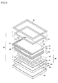
- Fig. 1 is a block diagram of an LCD device according to an exemplary embodiment of the present invention.
- Fig. 2 is an exploded perspective view schematically illustrating an LCD device according to an exemplary embodiment of the present invention.
- Fig. 3 is an equivalent circuit view of a pixel unit of an LCD device according to an exemplary embodiment of the present invention.
- an LCD device comprises an LC panel assembly 300, a gate driver 400 and a data driver 500 which are electrically connected to the LC panel assembly 300, a gray voltage generator 800 electrically connected to the data driver 400, a light source section 910 for supplying the light to the LC panel assembly 300, a light source driver 920 for controlling the light source section 910, and a signal controller 600 for controlling the above elements.
- the LCD device according to an exemplary embodiment of the present invention comprises an LC module 350 including a display unit 330 and a backlight 340, a front housing 361 and a rear housing 362 for receiving and supporting the LC module 350, and a first mold frame 363 and a second mold frame 364.
- the display unit 330 includes the LC panel assembly 300, a gate tape carrier package (TCP) 410 and a data TCP 510 which are attached to the LC panel assembly 300, and a gate printed circuit board (PCB) 450 and a data PCB 550 which are individually attached to the gate and data TCPs 410 and 510, respectively.
- TCP gate tape carrier package
- PCB gate printed circuit board
- the LC panel assembly 300 includes a lower panel 100 and an upper panel 200 facing each other, and an LC layer 3 disposed between the lower and upper panels 100 and 200.
- the LC panel assembly 300 includes display signal lines G 1 -G n and D 1 -D m and pixels connected to the display signal lines G 1 -G n and D 1 -D m and arranged substantially in a matrix.
- the display signal lines G 1 -G n and D 1 -D m are provided on the lower panel 100 and include gate lines G 1 -G n for transmitting gate signals (also referred to as "scanning signals"), and data lines D 1 -D m for transmitting data signals or data voltages.
- the gate lines G 1 -G n extend substantially in a row direction of the LC panel assembly 300 and are substantially parallel to each other, while the data lines D 1 -D m extend substantially in a column direction of the LC panel assembly 300 and are substantially parallel to each other.
- the switching element Q such as a thin film transistor (TFT) is provided on the lower panel 100 and has three terminals: a control terminal connected to one of the gate lines G 1 -G n ; an input terminal connected to one of the data lines D 1 -D m ; and an output terminal connected to both the LC capacitor C LC and the storage capacitor C ST.
- TFT thin film transistor
- the LC capacitor C LC includes a pixel electrode 190 provided on the lower panel 100 and a common electrode 270 provided on the upper panel 200 as two terminals.
- the LC layer 3 interposed between the pixel and common electrodes 190 and 270 functions as a dielectric of the LC capacitor C LC .
- the pixel electrode 190 is electrically connected to the switching element Q, and the common electrode 270 is supplied with a common voltage V com and covers an entire surface of the upper panel 200.
- the common electrode 270 may be provided on the lower panel 100. In such a case, at least one of the pixel electrode 190 and the common electrode 270 may be shaped as a bar or a stripe.
- the storage capacitor C ST is an auxiliary capacitor for the LC capacitor C LC .
- an overlap portion between the pixel electrode 190 and the separate signal line forms the storage capacitor C ST .
- the separate signal line is supplied with a predetermined voltage such as, for example, the common voltage V com .
- the storage capacitor C ST may be formed by an overlapping of the pixel electrode 190 and a previous gate line, which is placed directly before the pixel electrode 190, having an insulator therebetween.
- each pixel uniquely exhibits one of three primary colors (i.e., spatial division), or sequentially exhibits three primary colors in turn depending on time (i.e., temporal division), so that a spatial or temporal sum of the primary colors are recognized as a desired color.
- Fig. 3 shows an example of the spatial division, in which each pixel includes a color filter 230 for exhibiting one of the primary colors in an area of the upper panel 200 corresponding to the pixel electrode 190.
- the color filter 230 may be provided on or under the pixel electrode 190.
- the backlight 340 is mounted under the LC panel assembly 300.
- the backlight 340 comprises a light source unit 349 including light emitting diodes (LEDs) 344 arranged on a printed circuit board (PCB) 345, a light guiding plate 342 and optical sheets 343 which are provided between the LC panel assembly 300 and the LEDs 344 for dispersing light emitted from the LEDs 344 to the LC panel assembly 300.
- the backlight 340 further comprises a reflecting plate 341, which is disposed over the PCB 345 and includes holes corresponding to each of the LEDs 344.
- the LEDs 344 provide light to the LC panel assembly 300 and include white LEDs emitting white light and red LEDs emitting red light.
- the white and red LEDs are arranged on the PCB 345 in a predetermined arrangement, thereby forming the light source unit 349.
- Fig. 2 shows an example of a direct type backlight in which the light source units 349 are arranged parallel to each other below the LC panel assembly 300.
- An alternative to the direct type backlight shown in Fig. 2 includes an edge type backlight.
- the light source units 349 are arranged at one or more edges of the backlight 340, below the LC panel assembly 300 and light emitted by the light source units 349 is distributed to the LC panel assembly 300 by the light guiding plate 342.
- Polarizers (not shown) are provided on outer surfaces of the lower and upper panels 100 and 200 for polarizing light emitted by the light source units 349.
- the gray voltage generator 800 is included in the data PCB 550 and generates two sets of gray voltages related to a transmittance of the pixels.
- the gray voltages of a first set have a positive polarity with respect to the common voltage v com
- gray voltages of a second set have a negative polarity with respect to the common voltage v com .
- An exemplary embodiment of the present invention employs multiple gate drivers 400 and multiple gate TCPs 410.
- the gate drivers 400 are individually mounted on each gate TCP 410, having shapes of integrated circuit (IC) chips.
- the gate drivers 400 are individually connected to the gate lines G 1 -G n of the LC panel assembly 300 for transmitting the gate signals including combinations of a gate-on voltage V on and a gate-off voltage V off input from an external device.
- An exemplary embodiment of the present invention employs multiple data drivers 500 and multiple data TCPs 510.
- the data drivers 500 are individually mounted on each data TCP 510, having shapes of IC chips. Additionally, the data drivers 500 are individually connected to the data lines D 1 -D m of the LC panel assembly 300 for transmitting the data voltages which are selected from the gray voltages supplied from the gray voltage generator 800, to the data signal lines D 1 -D m .
- the gate driver 400 or the data driver 500 is directly mounted on the lower panel 100 having the shape of an IC chip. In still another embodiment of the present invention, the gate driver 400 or the data driver 500 is integrated into the lower panel 100 along with other elements. In each of the above cases, the gate or data PCB 450 or 550 or the gate or data TCP 410 or 510 can be omitted.
- the signal controller 600 may be included in the data PCB 550 or the gate PCB 450 for controlling an operation of the gate driver 400 or the data driver 500.
- the signal controller 600 receives input image signals R, G, and B and input control signals for controlling a display of the LCD device.
- the input control signals include a vertical synchronizing signal V sync, a horizontal synchronizing signal H sync, a main clock MCLK, a data enable signal DE, etc., all of which are provided from an external graphic controller (not shown).
- the signal controller 600 processes the input image signals R, G, and B suitably for operation of the LC panel assembly 300 and generates gate control signals CONT1 and data control signals CONT2, and then outputs the gate control signals CONT1 and the data control signals CONT2 to the gate driver 400 and the data driver 500, respectively.
- the gate control signals CONT1 include a vertical synchronizing start signal STV for informing the gate driver 400 of a beginning of a frame, a gate clock signal CPV for controlling an output time of the gate-on voltage V on , and an output enable signal OE for defining a duration of the gate-on voltage V on .
- the data control signals CONT2 include a horizontal synchronizing start signal STH for informing the data driver 500 of a beginning of a data transmission, a load signal LOAD for instructing the data driver 500 to apply the data voltages to the data lines D 1 -D m , a reverse signal RVS for reversing a polarity of the data voltages with respect to the common voltage V com , and a data clock signal HCLK.
- the data driver 500 Responsive to the data control signals CONT2 from the signal controller 600, the data driver 500 successively receives the image data DAT for a row of the pixels from the signal controller 600, shifts them, converts the processed image data DAT into analog data voltages selected from the gray voltages from the gray voltage generator 800, and then applies the data voltages to data lines D 1 -D m .
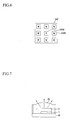
- the light source section 910 including the light source unit 349 for the backlight device according to an exemplary embodiment of the present invention will be described in detail with reference to Figs. 4, 5, and 6.
- Figs. 5 and 6 show alternative arrays of the white and red LEDs 344W and 344R.
- Each of Figs. 5 and 6 shows an LED array unit in which each LED array unit includes a plurality of white LEDs 344W surrounding one red LED 344R.
- Such LED array units may be configured on one PCB 345' and PCB 345" as shown in Figs. 5 and 6, or may be configured by linking a plurality of band-shaped PCBs 345 as shown in Fig. 4.
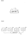
- an ultraviolet LED chip 12 is mounted on a lead frame 40, and is covered with red fluorescent material 22, green fluorescent material 23, and blue fluorescent material 24.
- a molding element 30 covers the red, green, and blue fluorescent materials 22, 23, and 24 and the lead frame 40.
- the red, green, and blue fluorescent materials 22, 23, and 24 convert ultraviolet light emitted by the ultraviolet LED chip 12 to red, green, and blue lights, respectively.
- white light is produced when the red, green, and blue lights converted by the red, green, and blue fluorescent materials 22, 23, and 24 are mixed.
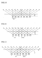
- Fig. 10 shows a minimum color mixing area required to produce white light from a backlight device according to an exemplary embodiment of the present invention.
- Fig. 11 shows a minimum color mixing area required to produce white light from a backlight device which utilizes a red, green, and blue LED array.
- Fig. 12 shows a minimum color mixing area required to produce white light from a backlight device which utilizes a red, green, green, and blue LED array.
- Equation 1 the period is a distance between two LEDs emitting the same light, and ⁇ is a half of a light emission angle of an LED.
- the gap between adjacent LEDs (p) is also called pitch.
- the critical length X is calculated by equation 2.
- the minimum color mixing area of the light source is two thirds that of a three color (red, green, and blue) LED array, and is half that of a four color (red, green, green, and blue) LED array.
- a space for a backlight device must be large enough to provide the minimum color mixing area having a critical length X as calculated above. Accordingly, a light source according to the exemplary embodiments of the present invention may be made thinner than the three or four color LED arrays, since the critical length X for the light source according to the exemplary embodiments of the present invention is smaller than the critical length X for the three or four color LED arrays. Thus the light source according to the exemplary embodiments of the present invention is more profitable in facilitating thin LCD devices due to a reduced backlight space requirement.
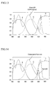
- Fig. 13 is a graph for comparison between a spectrum of white light emitted by ultraviolet LEDs and white LEDs using three-color fluorescent materials and spectrums of a complete white light passing through red R, green G, and blue B color filters of the LCD device.
- a complete white light refers to white light having substantially equal component wavelengths across a visible light spectrum.
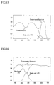
- Fig. 14 is a graph for comparison between a spectrum of white light emitted from a light source of a backlight device according to an exemplary embodiment of the present invention and corresponding spectrums of the complete white light passing through red, green, and blue color filters of the LCD device.
- white light emitted from the ultraviolet LEDs and the white LEDs using three-color fluorescent materials does not include light of all wavelength ranges, but partially includes light of blue, green, and red wavelength ranges.
- the spectrum of the white light emitted from the white LEDs has two peaks in the range of about 400nm to about 460nm corresponding to a blue area, a peak in the range of about 500nm to about 550nm corresponding to a green area, and a peak in the range of over about 600nm corresponding to a red area.
- Figs. 15 and 16 are graphs of spectrums for illustrating a principle for producing a more complete white light by using LEDs that emit insufficient white light together with a single-color-emitting LED as an exemplary embodiment of the present invention.
- the white LEDs 344W lacking a red component and the red LEDs 344R are used together to produce a more complete white light.
- a white light source lacking blue or green component, or the mixed-color-emitting LEDs lacking a particular color component wavelength is employed, a single-color-emitting LED capable of compensating for an insufficient component is added, thereby producing the complete white light.
- Fig. 15 shows spectrums when mixed-color-emitting LEDs without the red component and a red LED are used together
- Fig. 16 shows spectrums when a white LED lacking a wavelength component of about 450nm to about 500nm and the LED having wavelength of about 450nm to about 500nm are used together.
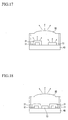
- the blue LED chip 11 and a red LED chip 13 are mounted on the lead frame 40.
- the blue LED chip 11 is covered with the yellow fluorescent material 21 and a molding element 30 covers all of the above-mentioned elements for protection.
- a structure shown in Fig. 18 includes two blue LED chips 11 each being covered by corresponding yellow fluorescent materials 21, and the red LED chip 13 disposed between the two blue LED chips 11.
- the red component is reduced as compared with the embodiment of Fig. 17.
- Integral packaging of a white LED and a red LED as shown in Figs. 17 and 18 minimizes space required for a light source in the LCD device since a color mixing area is not required, and simplifies LED array processes, improving productivity.
- a complete white light source can be obtained.
- Such constructed light sources are applicable for direct type backlights and edge type backlights.
- Edge type backlights will be described with reference to Figs. 19 to 22.
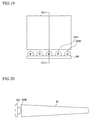
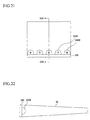
- Fig. 19 is a top-side view of an edge type backlight device according to another exemplary embodiment of the present invention and Fig. 20 is a cross-sectional view cut along line XX-XX' of Fig. 19.
- a PCB 345 mounting white LEDs 344W and red LEDs 344R thereon is provided at an edge of a wedge-shaped light guiding plate 50.
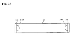
- Fig. 21 is a top-side view of an edge type backlight device according to still another exemplary embodiment of the present invention and Fig. 22 is a cross-sectional view cut along line XX II-XX II' of Fig. 21.
- a PCB 345 mounting white LEDs 344W and red LEDs 344R thereon is provided at an edge of the wedge-shaped light guiding plate 50.
- the wedge-shaped light guiding plate 50 includes grooves for receiving the white LEDs 344W and red LEDs 344R therein.
- two PCBs 345 mounting white LEDs 344W and red LEDs 344R thereon are individually provided at each opposite edge of a light guiding plate 50'.
- a flat panel-shaped light guiding plate 50' is used.
- the white LEDs 344W and red LEDs 344R used in the embodiments shown in Fig. 13 to Fig. 19, the white light source lacking blue or green component, or the mixed-color-emitting LEDs lacking a particular color component in the wavelength can be used together with the single-color-emitting LED capable of compensating the insufficient component.
- the space required for a light source using LEDs is reduced in the LCD device, and white light of acceptable quality can be produced.
Landscapes
- Physics & Mathematics (AREA)
- Nonlinear Science (AREA)
- Optics & Photonics (AREA)
- Crystallography & Structural Chemistry (AREA)
- Chemical & Material Sciences (AREA)
- General Physics & Mathematics (AREA)
- Mathematical Physics (AREA)
- Liquid Crystal (AREA)
- Planar Illumination Modules (AREA)
- Led Device Packages (AREA)
- Non-Portable Lighting Devices Or Systems Thereof (AREA)
- Led Devices (AREA)
- Light Guides In General And Applications Therefor (AREA)
Applications Claiming Priority (1)
| Application Number | Priority Date | Filing Date | Title |
|---|---|---|---|
| KR1020040049454A KR20060000544A (ko) | 2004-06-29 | 2004-06-29 | 표시 장치용 백라이트, 표시 장치용 광원, 광원용 발광다이오드 |
Publications (1)
| Publication Number | Publication Date |
|---|---|
| EP1619545A1 true EP1619545A1 (en) | 2006-01-25 |
Family
ID=34941752
Family Applications (1)
| Application Number | Title | Priority Date | Filing Date |
|---|---|---|---|
| EP05253892A Withdrawn EP1619545A1 (en) | 2004-06-29 | 2005-06-23 | Backlight for display device |
Country Status (5)
| Country | Link |
|---|---|
| US (1) | US7293907B2 (enExample) |
| EP (1) | EP1619545A1 (enExample) |
| JP (1) | JP2006019736A (enExample) |
| KR (1) | KR20060000544A (enExample) |
| CN (1) | CN1716347A (enExample) |
Families Citing this family (68)
| Publication number | Priority date | Publication date | Assignee | Title |
|---|---|---|---|---|
| KR101035502B1 (ko) * | 2004-11-16 | 2011-05-20 | 엘지디스플레이 주식회사 | 발광다이오드를 이용한 액정표시장치모듈 |
| US7316497B2 (en) * | 2005-03-29 | 2008-01-08 | 3M Innovative Properties Company | Fluorescent volume light source |
| KR100674850B1 (ko) * | 2005-05-02 | 2007-01-26 | 삼성전기주식회사 | 하이브리드 백라이트 장치 |
| KR100691191B1 (ko) * | 2005-07-15 | 2007-03-09 | 삼성전기주식회사 | Led를 이용한 면광원 및 이를 구비하는 lcd 백라이트유닛 |
| WO2007070821A2 (en) * | 2005-12-13 | 2007-06-21 | Ilight Technologies, Inc. | Illumination device with hue transformation |
| US7659544B2 (en) * | 2005-12-23 | 2010-02-09 | Hong Kong Applied Science And Technology Research Institute Co., Ltd. | Light emitting device with at least two alternately driven light emitting diodes |
| US7474287B2 (en) * | 2005-12-23 | 2009-01-06 | Hong Kong Applied Science And Technology | Light emitting device |
| US7659546B2 (en) | 2005-12-23 | 2010-02-09 | Hong Kong Applied Science And Technology Research Institute Co., Ltd. | Light emitting device |
| JP4980640B2 (ja) * | 2006-03-31 | 2012-07-18 | 三洋電機株式会社 | 照明装置 |
| KR100780187B1 (ko) * | 2006-04-06 | 2007-11-27 | 삼성전기주식회사 | Led를 이용한 액정표시장치용 백라이트 유닛 |
| WO2007125623A1 (ja) * | 2006-04-28 | 2007-11-08 | Sharp Kabushiki Kaisha | 照明装置およびこれを備えた液晶表示装置 |
| JP4585481B2 (ja) * | 2006-04-28 | 2010-11-24 | 株式会社 日立ディスプレイズ | Ledバックライト及びそれを用いた液晶表示装置 |
| JP4702167B2 (ja) * | 2006-05-09 | 2011-06-15 | 豊田合成株式会社 | 液晶ディスプレイ装置 |
| KR100820529B1 (ko) | 2006-05-11 | 2008-04-08 | 엘지이노텍 주식회사 | 발광 장치 및 그 제조방법, 면 발광 장치 |
| US20070280622A1 (en) * | 2006-06-02 | 2007-12-06 | 3M Innovative Properties Company | Fluorescent light source having light recycling means |
| US20070279914A1 (en) * | 2006-06-02 | 2007-12-06 | 3M Innovative Properties Company | Fluorescent volume light source with reflector |
| TWI342974B (en) * | 2006-07-06 | 2011-06-01 | Chimei Innolux Corp | Liquid crystal display and backlight module thereof |
| US7857457B2 (en) * | 2006-09-29 | 2010-12-28 | 3M Innovative Properties Company | Fluorescent volume light source having multiple fluorescent species |
| US10295147B2 (en) | 2006-11-09 | 2019-05-21 | Cree, Inc. | LED array and method for fabricating same |
| KR100819652B1 (ko) * | 2006-12-28 | 2008-04-04 | 우리이티아이 주식회사 | 엘이디 백라이트 장치 |
| CN100543555C (zh) * | 2006-12-29 | 2009-09-23 | 晶宏半导体股份有限公司 | 侧光源背光模块 |
| EP2109738B1 (en) * | 2007-01-18 | 2012-11-28 | Brandon Medical Company Limited | Illumination device |
| JP4996941B2 (ja) * | 2007-02-21 | 2012-08-08 | 富士フイルム株式会社 | 液晶表示装置 |
| JP4974703B2 (ja) * | 2007-02-21 | 2012-07-11 | 富士フイルム株式会社 | 面状照明装置 |
| US20080203948A1 (en) * | 2007-02-27 | 2008-08-28 | Unity Opto Technology Co., Ltd. | Lighting device |
| CN101681053B (zh) | 2007-05-20 | 2012-03-21 | 3M创新有限公司 | 具有半镜面元件的循环背光源 |
| CN101681057B (zh) | 2007-05-20 | 2012-07-04 | 3M创新有限公司 | 光循环型薄壁中空腔体背光源 |
| TWI448643B (zh) | 2007-05-20 | 2014-08-11 | 3M Innovative Properties Co | 背光與利用背光之顯示系統 |
| TWI439641B (zh) | 2007-05-20 | 2014-06-01 | 3M Innovative Properties Co | 用於側面發光型背光之準直光注入器 |
| US7905618B2 (en) * | 2007-07-19 | 2011-03-15 | Samsung Led Co., Ltd. | Backlight unit |
| KR100951274B1 (ko) * | 2007-07-19 | 2010-05-06 | 삼성엘이디 주식회사 | 백라이트 유닛 |
| KR100949194B1 (ko) * | 2007-08-08 | 2010-03-23 | 주식회사 우영 | Led 조명장치 |
| KR100966374B1 (ko) | 2007-08-27 | 2010-07-01 | 삼성엘이디 주식회사 | 백색 led를 이용한 면광원 및 이를 구비한 lcd백라이트 유닛 |
| GB0813834D0 (en) * | 2008-07-29 | 2008-09-03 | Brandon Medical Company Ltd | Illumination assembly |
| US9151884B2 (en) * | 2008-02-01 | 2015-10-06 | 3M Innovative Properties Company | Fluorescent volume light source with active chromphore |
| EP2255231A1 (en) | 2008-02-07 | 2010-12-01 | 3M Innovative Properties Company | Hollow backlight with structured films |
| WO2009105450A1 (en) | 2008-02-22 | 2009-08-27 | 3M Innovative Properties Company | Backlights having selected output light flux distributions and display systems using same |
| TW200950128A (en) * | 2008-05-16 | 2009-12-01 | Yu-Nung Shen | Light-emitting diode chip packaging body and its packaging method |
| EP2297607B1 (en) | 2008-06-04 | 2014-04-23 | 3M Innovative Properties Company | Hollow backlight with tilted light source |
| US9425172B2 (en) * | 2008-10-24 | 2016-08-23 | Cree, Inc. | Light emitter array |
| US8575865B2 (en) * | 2009-03-24 | 2013-11-05 | Apple Inc. | Temperature based white point control in backlights |
| US8390562B2 (en) * | 2009-03-24 | 2013-03-05 | Apple Inc. | Aging based white point control in backlights |
| US8378958B2 (en) * | 2009-03-24 | 2013-02-19 | Apple Inc. | White point control in backlights |
| DE102009024069A1 (de) * | 2009-06-05 | 2010-12-09 | Osram Opto Semiconductors Gmbh | Optisches Beleuchtungsgerät und optisches Aufzeichnungsgerät |
| US8704751B2 (en) | 2010-04-05 | 2014-04-22 | American Panel Corporation | Redundant power/control system for liquid crystal displays |
| US20120147293A1 (en) | 2010-06-11 | 2012-06-14 | Amercan Panel Corporation | Redundant backlight for liquid crystal displays |
| US20120044676A1 (en) * | 2010-08-19 | 2012-02-23 | Unity Opto Technology Co., Ltd. | Structure of light-emitting diode (LED) lamp |
| DE202010008480U1 (de) * | 2010-09-08 | 2011-12-09 | Zumtobel Lighting Gmbh | LED-Leuchte zur Erzeugung von weißem Licht |
| JP2012119252A (ja) * | 2010-12-03 | 2012-06-21 | Hitachi Consumer Electronics Co Ltd | 液晶表示装置 |
| KR20120080853A (ko) * | 2011-01-10 | 2012-07-18 | 삼성모바일디스플레이주식회사 | 디스플레이 모듈 |
| KR101905852B1 (ko) * | 2011-04-13 | 2018-10-08 | 엘지이노텍 주식회사 | 광학 시트 및 이를 포함하는 표시장치 |
| CN102155694B (zh) * | 2011-04-14 | 2012-10-10 | 深圳市华星光电技术有限公司 | 背光模块 |
| US8426877B2 (en) | 2011-04-14 | 2013-04-23 | Shenzhen China Star Optoelectronics Technology Co., Ltd. | Backlight module |
| US10842016B2 (en) | 2011-07-06 | 2020-11-17 | Cree, Inc. | Compact optically efficient solid state light source with integrated thermal management |
| WO2013094481A1 (ja) * | 2011-12-19 | 2013-06-27 | シャープ株式会社 | 照明装置、シーリングライト、バックライト、液晶表示装置、及びテレビジョン受信装置 |
| US9269697B2 (en) * | 2011-12-28 | 2016-02-23 | Ledengin, Inc. | System and methods for warm white LED light source |
| KR102035610B1 (ko) | 2012-06-20 | 2019-10-23 | 삼성전자주식회사 | 백색 광원 및 청색 광원을 구비한 백라이트 유닛과 이를 이용하는 디스플레이 패널 및 디스플레이 장치와 그 디스플레이 방법 |
| CN102901012B (zh) * | 2012-10-30 | 2014-12-10 | 京东方科技集团股份有限公司 | 背光模组及显示装置 |
| KR102013611B1 (ko) * | 2012-11-15 | 2019-08-23 | 엘지전자 주식회사 | 이동 단말기 |
| US9171509B2 (en) | 2013-04-19 | 2015-10-27 | VIZIO Inc. | Single backlight source where the backlight emits pure colored light in a sequential manner where the sequence is red, blue and green |
| JP6284738B2 (ja) * | 2013-10-18 | 2018-02-28 | シチズン電子株式会社 | 半導体発光装置 |
| CN103559849B (zh) | 2013-11-15 | 2016-08-17 | 北京京东方光电科技有限公司 | 显示面板的显示方法 |
| CN103901667B (zh) * | 2014-03-27 | 2017-09-12 | 深圳市华星光电技术有限公司 | 液晶显示装置 |
| WO2016072368A1 (ja) * | 2014-11-06 | 2016-05-12 | シャープ株式会社 | 照明装置及び表示装置 |
| CN205424603U (zh) * | 2015-11-27 | 2016-08-03 | 乐视致新电子科技(天津)有限公司 | 一种用于提高3d效果的背光装置 |
| CN107464531B (zh) * | 2017-07-31 | 2020-02-21 | 天津大学 | 利用lcd显示器背光源图像显示方法 |
| CN109493809B (zh) * | 2017-09-12 | 2021-01-01 | 纬创资通(中山)有限公司 | 显示装置以及背光驱动方法 |
| CN110767795B (zh) * | 2019-12-27 | 2020-05-05 | 华引芯(武汉)科技有限公司 | 一种微型led发光器件及其制备方法 |
Citations (4)
| Publication number | Priority date | Publication date | Assignee | Title |
|---|---|---|---|---|
| JP2000275636A (ja) * | 1999-03-25 | 2000-10-06 | Seiko Epson Corp | 光源及び照明装置並びにその照明装置を用いた液晶装置 |
| WO2001041215A1 (en) * | 1999-12-02 | 2001-06-07 | Koninklijke Philips Electronics N.V. | Hybrid white light source comprising led and phosphor-led |
| US20040021629A1 (en) * | 2002-07-18 | 2004-02-05 | Citizen Electronics Co., Ltd. | Light emitting diode device |
| DE10233050A1 (de) * | 2002-07-19 | 2004-02-05 | Osram Opto Semiconductors Gmbh | Lichtquelle auf LED-Basis, insbesondere für die Erzeugung von weißem Licht |
Family Cites Families (14)
| Publication number | Priority date | Publication date | Assignee | Title |
|---|---|---|---|---|
| TW408497B (en) * | 1997-11-25 | 2000-10-11 | Matsushita Electric Works Ltd | LED illuminating apparatus |
| TW500962B (en) | 1999-11-26 | 2002-09-01 | Sanyo Electric Co | Surface light source and method for adjusting its hue |
| JP2002075038A (ja) | 2000-09-05 | 2002-03-15 | Sony Corp | バックライトユニット及びこれを用いた液晶表示装置 |
| KR20020041479A (ko) | 2000-11-28 | 2002-06-03 | 유순재 | 엘씨디의 백 라이트 광원 모듈 |
| KR100788382B1 (ko) | 2000-12-13 | 2007-12-31 | 엘지.필립스 엘시디 주식회사 | 액정표시장치의 백라이트 유닛 |
| DE10102585A1 (de) | 2001-01-20 | 2002-07-25 | Philips Corp Intellectual Pty | Farbige Beleuchtungseinrichtung |
| JP2002231032A (ja) | 2001-02-02 | 2002-08-16 | Stanley Electric Co Ltd | 白色led光源バックライト装置 |
| JP2002270020A (ja) | 2001-03-08 | 2002-09-20 | Casio Comput Co Ltd | 光源装置 |
| JP2002350846A (ja) | 2001-05-22 | 2002-12-04 | Yazaki Corp | Ledバックライト |
| JP3988575B2 (ja) * | 2002-08-09 | 2007-10-10 | 株式会社デンソー | フルカラー表示装置 |
| KR20040029232A (ko) | 2002-09-25 | 2004-04-06 | 엘지.필립스 엘시디 주식회사 | 액정표시장치의 백라이트 유닛 |
| KR100546705B1 (ko) | 2002-09-25 | 2006-01-26 | 엘지.필립스 엘시디 주식회사 | 액정표시장치의 백라이트 유닛 |
| KR100546706B1 (ko) | 2002-09-26 | 2006-01-26 | 엘지.필립스 엘시디 주식회사 | 액정표시장치의 백라이트 유닛 |
| KR100628264B1 (ko) | 2002-09-26 | 2006-09-27 | 엘지.필립스 엘시디 주식회사 | 액정표시장치의 백라이트 유닛 |
-
2004
- 2004-06-29 KR KR1020040049454A patent/KR20060000544A/ko not_active Ceased
-
2005
- 2005-06-23 EP EP05253892A patent/EP1619545A1/en not_active Withdrawn
- 2005-06-28 CN CNA2005100813629A patent/CN1716347A/zh active Pending
- 2005-06-28 JP JP2005188965A patent/JP2006019736A/ja not_active Withdrawn
- 2005-06-29 US US11/169,528 patent/US7293907B2/en not_active Expired - Lifetime
Patent Citations (4)
| Publication number | Priority date | Publication date | Assignee | Title |
|---|---|---|---|---|
| JP2000275636A (ja) * | 1999-03-25 | 2000-10-06 | Seiko Epson Corp | 光源及び照明装置並びにその照明装置を用いた液晶装置 |
| WO2001041215A1 (en) * | 1999-12-02 | 2001-06-07 | Koninklijke Philips Electronics N.V. | Hybrid white light source comprising led and phosphor-led |
| US20040021629A1 (en) * | 2002-07-18 | 2004-02-05 | Citizen Electronics Co., Ltd. | Light emitting diode device |
| DE10233050A1 (de) * | 2002-07-19 | 2004-02-05 | Osram Opto Semiconductors Gmbh | Lichtquelle auf LED-Basis, insbesondere für die Erzeugung von weißem Licht |
Non-Patent Citations (1)
| Title |
|---|
| PATENT ABSTRACTS OF JAPAN vol. 2000, no. 13 5 February 2001 (2001-02-05) * |
Also Published As
| Publication number | Publication date |
|---|---|
| JP2006019736A (ja) | 2006-01-19 |
| US20050286264A1 (en) | 2005-12-29 |
| KR20060000544A (ko) | 2006-01-06 |
| US7293907B2 (en) | 2007-11-13 |
| CN1716347A (zh) | 2006-01-04 |
Similar Documents
| Publication | Publication Date | Title |
|---|---|---|
| US7293907B2 (en) | Backlight for display device, light source for display device, and light emitting diode used therefor | |
| US7306357B2 (en) | Line light source using light emitting diode and lens and backlight unit using the same | |
| US8368846B2 (en) | Two dimensional light source using light emitting diode and liquid crystal display device using the two dimensional light source | |
| US7585083B2 (en) | Backlight for display device | |
| US7549781B2 (en) | Light emitting diode and lens for the same | |
| US7633577B2 (en) | Light emitting diode backlight unit and liquid crystal display device using the same | |
| KR101171186B1 (ko) | 고휘도 발광 다이오드 및 이를 이용한 액정 표시 장치 | |
| US20070236447A1 (en) | Backlight unit using light emitting diode | |
| EP1653254A2 (en) | Light emitting diode and lens for the same | |
| US20080074902A1 (en) | Lcd backlight assembly with leds | |
| KR101706578B1 (ko) | 백라이트 유닛 및 이를 포함하는 액정표시장치 모듈 | |
| US20080144334A1 (en) | Light emitting diode package, and light source unit and backlight unit including the same | |
| US20090168456A1 (en) | Light source module for a display device and a display device having the same | |
| US8692265B2 (en) | Lighting device | |
| JP5294667B2 (ja) | 液晶表示装置 | |
| KR20090080196A (ko) | 백라이트 유닛 및 이를 포함하는 표시 장치 | |
| US20120175650A1 (en) | Illuminating device and display device | |
| KR20120036660A (ko) | 백라이트 유닛 및 이를 포함하는 액정표시장치 | |
| US20160363818A1 (en) | Liquid crystal display device | |
| KR100685433B1 (ko) | 액정 표시 장치 | |
| US20070234166A1 (en) | Inverter and display device having the same | |
| US7502080B2 (en) | Liquid crystal display and manufacturing method thereof | |
| US20130009558A1 (en) | Backlight unit | |
| JP2010277853A (ja) | バックライト | |
| US20070081355A1 (en) | Light generating unit, display device having the same, and method thereof |
Legal Events
| Date | Code | Title | Description |
|---|---|---|---|
| PUAI | Public reference made under article 153(3) epc to a published international application that has entered the european phase |
Free format text: ORIGINAL CODE: 0009012 |
|
| AK | Designated contracting states |
Kind code of ref document: A1 Designated state(s): AT BE BG CH CY CZ DE DK EE ES FI FR GB GR HU IE IS IT LI LT LU MC NL PL PT RO SE SI SK TR |
|
| AX | Request for extension of the european patent |
Extension state: AL BA HR LV MK YU |
|
| 17P | Request for examination filed |
Effective date: 20060712 |
|
| 17Q | First examination report despatched |
Effective date: 20060809 |
|
| AKX | Designation fees paid |
Designated state(s): GB |
|
| REG | Reference to a national code |
Ref country code: DE Ref legal event code: 8566 |
|
| STAA | Information on the status of an ep patent application or granted ep patent |
Free format text: STATUS: THE APPLICATION IS DEEMED TO BE WITHDRAWN |
|
| 18D | Application deemed to be withdrawn |
Effective date: 20101231 |