EP1608006A1 - Filmerzeugungsvorrichtung - Google Patents
Filmerzeugungsvorrichtung Download PDFInfo
- Publication number
- EP1608006A1 EP1608006A1 EP04722958A EP04722958A EP1608006A1 EP 1608006 A1 EP1608006 A1 EP 1608006A1 EP 04722958 A EP04722958 A EP 04722958A EP 04722958 A EP04722958 A EP 04722958A EP 1608006 A1 EP1608006 A1 EP 1608006A1
- Authority
- EP
- European Patent Office
- Prior art keywords
- unit
- deposition
- substrate
- annealing
- gas
- Prior art date
- Legal status (The legal status is an assumption and is not a legal conclusion. Google has not performed a legal analysis and makes no representation as to the accuracy of the status listed.)
- Withdrawn
Links
Images






Classifications
-
- H—ELECTRICITY
- H10—SEMICONDUCTOR DEVICES; ELECTRIC SOLID-STATE DEVICES NOT OTHERWISE PROVIDED FOR
- H10P—GENERIC PROCESSES OR APPARATUS FOR THE MANUFACTURE OR TREATMENT OF DEVICES COVERED BY CLASS H10
- H10P14/00—Formation of materials, e.g. in the shape of layers or pillars
- H10P14/20—Formation of materials, e.g. in the shape of layers or pillars of semiconductor materials
-
- H—ELECTRICITY
- H10—SEMICONDUCTOR DEVICES; ELECTRIC SOLID-STATE DEVICES NOT OTHERWISE PROVIDED FOR
- H10P—GENERIC PROCESSES OR APPARATUS FOR THE MANUFACTURE OR TREATMENT OF DEVICES COVERED BY CLASS H10
- H10P14/00—Formation of materials, e.g. in the shape of layers or pillars
- H10P14/60—Formation of materials, e.g. in the shape of layers or pillars of insulating materials
- H10P14/63—Formation of materials, e.g. in the shape of layers or pillars of insulating materials characterised by the formation processes
- H10P14/6326—Deposition processes
- H10P14/6328—Deposition from the gas or vapour phase
- H10P14/6334—Deposition from the gas or vapour phase using decomposition or reaction of gaseous or vapour phase compounds, i.e. chemical vapour deposition
- H10P14/6339—Deposition from the gas or vapour phase using decomposition or reaction of gaseous or vapour phase compounds, i.e. chemical vapour deposition deposition by cyclic CVD, e.g. ALD, ALE or pulsed CVD
-
- C—CHEMISTRY; METALLURGY
- C23—COATING METALLIC MATERIAL; COATING MATERIAL WITH METALLIC MATERIAL; CHEMICAL SURFACE TREATMENT; DIFFUSION TREATMENT OF METALLIC MATERIAL; COATING BY VACUUM EVAPORATION, BY SPUTTERING, BY ION IMPLANTATION OR BY CHEMICAL VAPOUR DEPOSITION, IN GENERAL; INHIBITING CORROSION OF METALLIC MATERIAL OR INCRUSTATION IN GENERAL
- C23C—COATING METALLIC MATERIAL; COATING MATERIAL WITH METALLIC MATERIAL; SURFACE TREATMENT OF METALLIC MATERIAL BY DIFFUSION INTO THE SURFACE, BY CHEMICAL CONVERSION OR SUBSTITUTION; COATING BY VACUUM EVAPORATION, BY SPUTTERING, BY ION IMPLANTATION OR BY CHEMICAL VAPOUR DEPOSITION, IN GENERAL
- C23C16/00—Chemical coating by decomposition of gaseous compounds, without leaving reaction products of surface material in the coating, i.e. chemical vapour deposition [CVD] processes
- C23C16/44—Chemical coating by decomposition of gaseous compounds, without leaving reaction products of surface material in the coating, i.e. chemical vapour deposition [CVD] processes characterised by the method of coating
- C23C16/455—Chemical coating by decomposition of gaseous compounds, without leaving reaction products of surface material in the coating, i.e. chemical vapour deposition [CVD] processes characterised by the method of coating characterised by the method used for introducing gases into reaction chamber or for modifying gas flows in reaction chamber
- C23C16/45523—Pulsed gas flow or change of composition over time
- C23C16/45525—Atomic layer deposition [ALD]
- C23C16/45527—Atomic layer deposition [ALD] characterized by the ALD cycle, e.g. different flows or temperatures during half-reactions, unusual pulsing sequence, use of precursor mixtures or auxiliary reactants or activations
-
- C—CHEMISTRY; METALLURGY
- C23—COATING METALLIC MATERIAL; COATING MATERIAL WITH METALLIC MATERIAL; CHEMICAL SURFACE TREATMENT; DIFFUSION TREATMENT OF METALLIC MATERIAL; COATING BY VACUUM EVAPORATION, BY SPUTTERING, BY ION IMPLANTATION OR BY CHEMICAL VAPOUR DEPOSITION, IN GENERAL; INHIBITING CORROSION OF METALLIC MATERIAL OR INCRUSTATION IN GENERAL
- C23C—COATING METALLIC MATERIAL; COATING MATERIAL WITH METALLIC MATERIAL; SURFACE TREATMENT OF METALLIC MATERIAL BY DIFFUSION INTO THE SURFACE, BY CHEMICAL CONVERSION OR SUBSTITUTION; COATING BY VACUUM EVAPORATION, BY SPUTTERING, BY ION IMPLANTATION OR BY CHEMICAL VAPOUR DEPOSITION, IN GENERAL
- C23C16/00—Chemical coating by decomposition of gaseous compounds, without leaving reaction products of surface material in the coating, i.e. chemical vapour deposition [CVD] processes
- C23C16/44—Chemical coating by decomposition of gaseous compounds, without leaving reaction products of surface material in the coating, i.e. chemical vapour deposition [CVD] processes characterised by the method of coating
- C23C16/455—Chemical coating by decomposition of gaseous compounds, without leaving reaction products of surface material in the coating, i.e. chemical vapour deposition [CVD] processes characterised by the method of coating characterised by the method used for introducing gases into reaction chamber or for modifying gas flows in reaction chamber
- C23C16/45523—Pulsed gas flow or change of composition over time
- C23C16/45525—Atomic layer deposition [ALD]
- C23C16/45527—Atomic layer deposition [ALD] characterized by the ALD cycle, e.g. different flows or temperatures during half-reactions, unusual pulsing sequence, use of precursor mixtures or auxiliary reactants or activations
- C23C16/45529—Atomic layer deposition [ALD] characterized by the ALD cycle, e.g. different flows or temperatures during half-reactions, unusual pulsing sequence, use of precursor mixtures or auxiliary reactants or activations specially adapted for making a layer stack of alternating different compositions or gradient compositions
-
- C—CHEMISTRY; METALLURGY
- C23—COATING METALLIC MATERIAL; COATING MATERIAL WITH METALLIC MATERIAL; CHEMICAL SURFACE TREATMENT; DIFFUSION TREATMENT OF METALLIC MATERIAL; COATING BY VACUUM EVAPORATION, BY SPUTTERING, BY ION IMPLANTATION OR BY CHEMICAL VAPOUR DEPOSITION, IN GENERAL; INHIBITING CORROSION OF METALLIC MATERIAL OR INCRUSTATION IN GENERAL
- C23C—COATING METALLIC MATERIAL; COATING MATERIAL WITH METALLIC MATERIAL; SURFACE TREATMENT OF METALLIC MATERIAL BY DIFFUSION INTO THE SURFACE, BY CHEMICAL CONVERSION OR SUBSTITUTION; COATING BY VACUUM EVAPORATION, BY SPUTTERING, BY ION IMPLANTATION OR BY CHEMICAL VAPOUR DEPOSITION, IN GENERAL
- C23C16/00—Chemical coating by decomposition of gaseous compounds, without leaving reaction products of surface material in the coating, i.e. chemical vapour deposition [CVD] processes
- C23C16/56—After-treatment
-
- H—ELECTRICITY
- H10—SEMICONDUCTOR DEVICES; ELECTRIC SOLID-STATE DEVICES NOT OTHERWISE PROVIDED FOR
- H10P—GENERIC PROCESSES OR APPARATUS FOR THE MANUFACTURE OR TREATMENT OF DEVICES COVERED BY CLASS H10
- H10P14/00—Formation of materials, e.g. in the shape of layers or pillars
- H10P14/60—Formation of materials, e.g. in the shape of layers or pillars of insulating materials
- H10P14/65—Formation of materials, e.g. in the shape of layers or pillars of insulating materials characterised by treatments performed before or after the formation of the materials
- H10P14/6516—Formation of materials, e.g. in the shape of layers or pillars of insulating materials characterised by treatments performed before or after the formation of the materials of treatments performed after formation of the materials
- H10P14/6529—Formation of materials, e.g. in the shape of layers or pillars of insulating materials characterised by treatments performed before or after the formation of the materials of treatments performed after formation of the materials by exposure to a gas or vapour
-
- H—ELECTRICITY
- H10—SEMICONDUCTOR DEVICES; ELECTRIC SOLID-STATE DEVICES NOT OTHERWISE PROVIDED FOR
- H10P—GENERIC PROCESSES OR APPARATUS FOR THE MANUFACTURE OR TREATMENT OF DEVICES COVERED BY CLASS H10
- H10P14/00—Formation of materials, e.g. in the shape of layers or pillars
- H10P14/60—Formation of materials, e.g. in the shape of layers or pillars of insulating materials
- H10P14/69—Inorganic materials
- H10P14/692—Inorganic materials composed of oxides, glassy oxides or oxide-based glasses
- H10P14/6938—Inorganic materials composed of oxides, glassy oxides or oxide-based glasses the material containing at least one metal element, e.g. metal oxides, metal oxynitrides or metal oxycarbides
- H10P14/6939—Inorganic materials composed of oxides, glassy oxides or oxide-based glasses the material containing at least one metal element, e.g. metal oxides, metal oxynitrides or metal oxycarbides characterised by the metal
-
- H—ELECTRICITY
- H10—SEMICONDUCTOR DEVICES; ELECTRIC SOLID-STATE DEVICES NOT OTHERWISE PROVIDED FOR
- H10P—GENERIC PROCESSES OR APPARATUS FOR THE MANUFACTURE OR TREATMENT OF DEVICES COVERED BY CLASS H10
- H10P14/00—Formation of materials, e.g. in the shape of layers or pillars
- H10P14/60—Formation of materials, e.g. in the shape of layers or pillars of insulating materials
- H10P14/69—Inorganic materials
- H10P14/692—Inorganic materials composed of oxides, glassy oxides or oxide-based glasses
- H10P14/6938—Inorganic materials composed of oxides, glassy oxides or oxide-based glasses the material containing at least one metal element, e.g. metal oxides, metal oxynitrides or metal oxycarbides
- H10P14/6939—Inorganic materials composed of oxides, glassy oxides or oxide-based glasses the material containing at least one metal element, e.g. metal oxides, metal oxynitrides or metal oxycarbides characterised by the metal
- H10P14/69391—Inorganic materials composed of oxides, glassy oxides or oxide-based glasses the material containing at least one metal element, e.g. metal oxides, metal oxynitrides or metal oxycarbides characterised by the metal the material containing aluminium, e.g. Al2O3
-
- H—ELECTRICITY
- H10—SEMICONDUCTOR DEVICES; ELECTRIC SOLID-STATE DEVICES NOT OTHERWISE PROVIDED FOR
- H10P—GENERIC PROCESSES OR APPARATUS FOR THE MANUFACTURE OR TREATMENT OF DEVICES COVERED BY CLASS H10
- H10P14/00—Formation of materials, e.g. in the shape of layers or pillars
- H10P14/60—Formation of materials, e.g. in the shape of layers or pillars of insulating materials
- H10P14/69—Inorganic materials
- H10P14/692—Inorganic materials composed of oxides, glassy oxides or oxide-based glasses
- H10P14/6938—Inorganic materials composed of oxides, glassy oxides or oxide-based glasses the material containing at least one metal element, e.g. metal oxides, metal oxynitrides or metal oxycarbides
- H10P14/6939—Inorganic materials composed of oxides, glassy oxides or oxide-based glasses the material containing at least one metal element, e.g. metal oxides, metal oxynitrides or metal oxycarbides characterised by the metal
- H10P14/69392—Inorganic materials composed of oxides, glassy oxides or oxide-based glasses the material containing at least one metal element, e.g. metal oxides, metal oxynitrides or metal oxycarbides characterised by the metal the material containing hafnium, e.g. HfO2
-
- H—ELECTRICITY
- H10—SEMICONDUCTOR DEVICES; ELECTRIC SOLID-STATE DEVICES NOT OTHERWISE PROVIDED FOR
- H10P—GENERIC PROCESSES OR APPARATUS FOR THE MANUFACTURE OR TREATMENT OF DEVICES COVERED BY CLASS H10
- H10P14/00—Formation of materials, e.g. in the shape of layers or pillars
- H10P14/60—Formation of materials, e.g. in the shape of layers or pillars of insulating materials
- H10P14/69—Inorganic materials
- H10P14/692—Inorganic materials composed of oxides, glassy oxides or oxide-based glasses
- H10P14/6938—Inorganic materials composed of oxides, glassy oxides or oxide-based glasses the material containing at least one metal element, e.g. metal oxides, metal oxynitrides or metal oxycarbides
- H10P14/6939—Inorganic materials composed of oxides, glassy oxides or oxide-based glasses the material containing at least one metal element, e.g. metal oxides, metal oxynitrides or metal oxycarbides characterised by the metal
- H10P14/69393—Inorganic materials composed of oxides, glassy oxides or oxide-based glasses the material containing at least one metal element, e.g. metal oxides, metal oxynitrides or metal oxycarbides characterised by the metal the material containing tantalum, e.g. Ta2O5
-
- H—ELECTRICITY
- H10—SEMICONDUCTOR DEVICES; ELECTRIC SOLID-STATE DEVICES NOT OTHERWISE PROVIDED FOR
- H10P—GENERIC PROCESSES OR APPARATUS FOR THE MANUFACTURE OR TREATMENT OF DEVICES COVERED BY CLASS H10
- H10P14/00—Formation of materials, e.g. in the shape of layers or pillars
- H10P14/60—Formation of materials, e.g. in the shape of layers or pillars of insulating materials
- H10P14/69—Inorganic materials
- H10P14/692—Inorganic materials composed of oxides, glassy oxides or oxide-based glasses
- H10P14/6938—Inorganic materials composed of oxides, glassy oxides or oxide-based glasses the material containing at least one metal element, e.g. metal oxides, metal oxynitrides or metal oxycarbides
- H10P14/6939—Inorganic materials composed of oxides, glassy oxides or oxide-based glasses the material containing at least one metal element, e.g. metal oxides, metal oxynitrides or metal oxycarbides characterised by the metal
- H10P14/69395—Inorganic materials composed of oxides, glassy oxides or oxide-based glasses the material containing at least one metal element, e.g. metal oxides, metal oxynitrides or metal oxycarbides characterised by the metal the material containing zirconium, e.g. ZrO2
-
- H—ELECTRICITY
- H10—SEMICONDUCTOR DEVICES; ELECTRIC SOLID-STATE DEVICES NOT OTHERWISE PROVIDED FOR
- H10P—GENERIC PROCESSES OR APPARATUS FOR THE MANUFACTURE OR TREATMENT OF DEVICES COVERED BY CLASS H10
- H10P14/00—Formation of materials, e.g. in the shape of layers or pillars
- H10P14/60—Formation of materials, e.g. in the shape of layers or pillars of insulating materials
- H10P14/69—Inorganic materials
- H10P14/692—Inorganic materials composed of oxides, glassy oxides or oxide-based glasses
- H10P14/6938—Inorganic materials composed of oxides, glassy oxides or oxide-based glasses the material containing at least one metal element, e.g. metal oxides, metal oxynitrides or metal oxycarbides
- H10P14/69398—Inorganic materials composed of oxides, glassy oxides or oxide-based glasses the material containing at least one metal element, e.g. metal oxides, metal oxynitrides or metal oxycarbides the material having a perovskite structure, e.g. BaTiO3
Definitions
- the invention relates to a deposition system which is capable of forming a metal compound thin film by atomic layer.
- High dielectric constant thin films are formed by such methods as CVD (Chemical Vapor Deposition), ALD (Atomic layer deposition), and sputtering.
- CVD Chemical Vapor Deposition
- ALD Atomic layer deposition
- sputtering a method for forming a thin film by cyclic supply of reactants for chemical substitution, not by thermal decomposition.
- This method provides a superior capability for split-level coating as compared to physical deposition methods such as sputtering, and also allows low-temperature processes. It is thus considered as a promising method for forming a high dielectric constant thin film to constitute a semiconductor device (for example, see Japanese Laid-Open Patent Applications 2001-152339, 2001-254181, and 2002-314072).
- a system for conducting this ALD-based deposition appears in Japanese Laid-Open Patent Application 2001-254181.
- This deposition system is one for achieving the process of supplying a first source gas to a substrate placed in a deposition chamber, purging this source gas, and then supplying a second source gas thereto. Switching the source gases and the purge gas alternately at speed allows deposition through the foregoing process, whereby atomic layers can be deposited layer by layer.
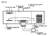
- Fig. 14 is a diagram schematically showing the structure of this ALD system.
- the same document describes that when the ALD system deposits Al 2 O 3 on a silicon substrate, terminating hydrogen on the silicon surface shall be desorbed. For example, this hydrogen desorption process is performed in an atmosphere of 400°C or above in temperature, whereas Al 2 O 3 is deposited at around 300°C.
- the sample When these processes are performed continuously in an ordinary ALD system, the sample must be once raised to 400°C or above in temperature for the sake of the hydrogen desorption process, and then the deposition is performed after a wait until the sample temperature falls to around 300°C. Then, performing the series of operations wafer by wafer increases the number of processes of the ALD system, thereby making the cost of the semiconductor device higher.
- the deposition system shown in Fig. 14 is to address this problem.
- the ALD system has a sample introduction chamber 13 which accommodates to-be-processed and processed samples, a reaction chamber 12 where depositing a predetermined film on a sample is carried out, and a conveyor system which conveys the samples in succession.
- the ALD system is also provided with a hydrogen desorption chamber 11 which performs the hydrogen desorption process.
- the hydrogen desorption process is carried out by using a heating lamp 16.
- This configuration allows the hydrogen desorption process and the deposition of the dielectric film, having different processing temperatures, to be performed continuously. Because of the provision of the respective chambers for performing the deposition processing and the preprocessing, it is possible to perform the processes continuously without waiting for the temperature to settle. Then, it has been concluded that the number of processes of the semiconductor device can be decreased to reduce the manufacturing cost of the semiconductor device.
- any of the deposition systems for performing such ALD-based deposition is basically configured so that a source gas and a purge gas are supplied alternately.
- a typical ALD deposition process to be achieved by these deposition systems will be described with reference to Fig. 1.
- the description will deal with the case of an aluminum oxide film.
- TMA trimethyl aluminum
- the material A is exhausted from the reaction chamber by inactive gas purging (S102).
- a reactive gas is supplied to the reaction chamber (S103).
- the reactive gas may be oxygen, water vapor, or the like.
- an oxygen atomic layer is formed on the atomic layer made of the material A.
- inactive gas purging is then performed to exhaust the air (S104).
- steps S101 to S104 are repeated to form a high dielectric constant thin film. Subsequently, whether a predetermined thickness is reached or not is checked by a thickness measuring device which is arranged on the deposition system (S107). If it is confirmed that the predetermined thickness is reached (Yes at S107), then thermal annealing is performed for the sake of film refining processing (S108). This thermal annealing is performed after the completion of the layer formation (Japanese Laid-Open Patent Application No. 2001-152339, paragraph 0047). This completes the deposition steps.
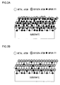
- Figs. 2A and 2B are schematic diagrams showing the layer structure of a high dielectric constant thin film formed by the steps of Fig. 1.
- Figs. 2A and 2B correspond to the states before and after the film refining processing by the thermal annealing shown in S108 of Fig. 1, respectively.
- impurities are distributed throughout the high dielectric constant thin film. After the annealing, impurities are removed from the entire film. The film is also densified. Nevertheless, in the lower areas of the high dielectric constant thin film or near the substrate in particular, impurities tend to be removed insufficiently and remain intact. In addition, since metal oxides are typically prone to crystallization, the film can be partially crystallized in the annealed state of Fig. 2B. The residual impurities and the film crystallization described above may contribute to deterioration in the characteristics of the device that contains the high dielectric constant thin film. For example, when the high dielectric constant thin film is applied to the gate insulating film of a transistor, it may cause an increase in leak current, deviations in threshold characteristics, etc.
- the present invention has been achieved in view of the foregoing problems. It is thus an object of the present invention to provide a deposition system which suppresses impurity contamination and film defects so that a thin film of favorable quality is obtained stably by ALD. Another object of the present invention is to provide a deposition system which is capable of introducing a different type of component into the thin film in a desired distribution.
- the present invention provides a deposition system which supplies a source gas and a purge gas alternately for deposition, comprising: a deposition chamber; a substrate holding unit which holds a substrate in the deposition chamber; a source gas supply unit which supplies the source gas to the deposition chamber; a reactive gas supply unit which supplies a reactive gas to the deposition chamber; a purge gas supply unit which supplies the purge gas to the deposition chamber; an exhaust unit which exhausts the source gas, the reactive gas, and the purge gas from the deposition chamber; a first heating unit which heats the substrate arranged in the deposition chamber to maintain the same to a predetermined temperature; and a second heating unit which heats the substrate arranged in the deposition chamber rapidly.
- the "reactive gas” refers to a gas that reacts with a metal to form a metal oxide or a metal nitride.
- the deposition system according to the present invention has the first and second heating units which heat the substrate arranged in the deposition chamber.
- the first heating unit can be used to maintain the substrate at a deposition temperature for depositing an atomic layer
- the second heating unit can be used to heat the substrate rapidly. It is therefore possible to perform both an atomic layer deposition step and an annealing step in the same deposition chamber without taking out the substrate.
- the two steps can also be switched quickly for deposition. Specifically, it is possible to achieve the deposition process of forming a layer by atomic layer deposition, performing annealing, and forming a layer again.
- the layer forming step When the layer forming step is suspended to interpose annealing, impurities mixed in the layer and defects of the layer can be removed sufficiently.
- the film can also be densified.
- an annealing gas such as ammonia can be introduced to form a nitrogen-introduced layer or the like inside the thin film freely through annealing.
- the deposited substrate has been taken out of the deposition system and loaded into another system for annealing.
- the atomic layer and the annealing can be performed in the same deposition system. The deposition process described above can thus be achieved stably.
- the source gas, the reactive gas, or the purge gas may be introduced in a direction parallel to the surface of the substrate.
- the surface of the substrate can be supplied with those gases efficiently so that a thin film of favorable quality is obtained stably.
- the first heating unit and the second heating unit may be opposed to each other with the substrate interposed therebetween, so that the first heating unit heats the substrate from the backside and the second heating unit heats the substrate from the surface.
- the surface of the substrate refers to the side to be subjected to deposition.
- the deposition system may further comprise an annealing gas introducing unit which introduces an annealing gas to the deposition chamber.
- an annealing gas introducing unit which introduces an annealing gas to the deposition chamber. This allows the process of forming a nitrogen-introduced layer or the like in a desired position inside the thin film through annealing as described above.
- an oxidant gas, a reductant gas, or the like can be introduced as the annealing gas during annealing, whereby impurities can be removed efficiently.
- the second heating unit may be an RTP (Rapid Thermal Processing) unit such as an infrared lamp, a laser annealing unit, and a flashing unit.
- RTP Rapid Thermal Processing
- the rapid heating of the substrate can be conducted stably, so that the process of repeating the atomic layer deposition and the annealing in succession can be conducted stably.
- the second heating unit may be arranged outside the deposition chamber. This can effectively suppress contamination of the second heating unit with the source gas, the reactive gas, and the like.
- the first heating unit may be a heater formed on a substrate holding surface of the substrate holding unit, for example. This makes it possible to heat the backside of the substrate by heat conduction or radiation. The substrate can thus be maintained at the deposition temperature stably.
- the configuration capable of purging quicker than in conventional systems allows the substrate temperature to be cooled rapidly. After annealing, it is thus possible to cool the substrate rapidly and switch to the next atomic layer deposition step speedily. Consequently, both the deposition and the annealing can be performed in the same deposition chamber. This achieves a deposition system which suitably suppresses impurity contamination and film defects. Moreover, since the process of forming a nitrogen-introduced layer or the like in a desired position inside the thin film through annealing becomes feasible, a different type of component can be introduced into the thin film in a desired distribution with reliability. This makes it possible to form a high-quality film having a desired component distribution stably.
- the substrate holding unit may have a moving mechanism which moves the substrate in position so that the distance between the substrate and the second heating unit can be adjusted by an operation from outside the deposition chamber without opening the deposition chamber.
- a high-flow purge gas supply unit and a corresponding exhaust unit may also be provided so that the rapid heating and rapid cooling of the substrate can be performed more smoothly.
- the deposition system may further comprise an annealing gas introducing unit which introduces an annealing gas into the deposition chamber.
- the substrate or the substrate holding unit may section the deposition chamber into a first chamber having the annealing gas introducing unit and a second chamber having the source gas supply unit and the reactive gas supply unit so that the surface of the substrate is exposed to the first chamber.
- the annealing is performed in part of the internal space of the deposition chamber. This further improves the temperature controllability in the process of rapid heating.
- the substrate need not be moved from the deposition chamber to a separate annealing chamber. The operations from the deposition to the annealing can be performed continuously in the deposition chamber.
- the source gas supply unit and the reactive gas supply unit can be arranged outside the small chambers for the sake of an improvement to the durability of the deposition system.
- the annealing gas is mixed with the source gas or the reactive gas, there may occur a corrosive gas which sometimes corrodes the inner walls of the deposition chamber.
- the foregoing configuration can thus be adopted to suppress the production of such a corrosive gas, thereby improving the durability of the deposition chamber.
- the first and second chambers may be formed inside the deposition chamber in various possible modes.
- the substrate holding unit and the inner walls of the deposition chamber may form a first chamber of enclosed structure when the substrate is put closer to the second heating unit.
- This simple configuration can form the small chambers inside the deposition chamber easily, and allows more efficient heating by the second heating unit.
- a partition member may be arranged inside the deposition chamber.
- the substrate or the substrate holding unit may be combined with the partition member to form a division wall inside the deposition chamber, thereby forming the first and second chambers. This can suppress the flow of the annealing gas into the second chamber, whereby corrosion of the inner walls of the deposition chamber is suppressed with reliability. Since the flow of the reactive gas into the first chamber is also suppressed, it is possible to suppress chemical reactions other than intended during annealing.
- the deposition system of the present invention may have a control unit which controls the operation of the second heating unit and the moving mechanism.
- the control unit may be configured to start heating the substrate by using the second heating unit after the substrate is put closer to the second heating unit by the moving mechanism. This makes it possible to heat the substrate even more efficiently.
- the deposition system of the present invention may further comprise: an annealing gas introducing unit which introduces an annealing gas to the deposition chamber; and a control unit which controls the operation of the second heating unit, the annealing gas introducing unit, and the moving mechanism.
- the control unit may be configured to start heating the substrate by using the second heating unit and introduce the annealing gas to the deposition chamber from the annealing gas introducing unit when the substrate is put closer to the second heating unit by the moving mechanism. This makes it possible to form a high-quality film with still higher reliability at speed.
- the exhaust unit may also be controlled by the control unit so that it can exhaust air from the entire deposition chamber when the substrate is put away from the second heating unit by the moving mechanism. Consequently, the entire deposition chamber including the area that makes the small chamber when the substrate is put closer to the second heating unit can be exhausted simultaneously. This makes it possible to perform gas replacement and cooling inside the deposition chamber with reliability at higher speed.
- the deposition system of the present invention is suitably used to form a metal compound layer made of a high dielectric constant material so-called high-k.
- the thin film may have a dielectric constant k of 8 or higher, for example.
- the metal compound layer may contain one or more elements selected from the group consisting of Hf, Zr, Al, La, Y, Si, Ba, Sr, Ti, Pb, Bi, Ta, Nb, and Mn. Among these, any of Hf, Zr, Al, La, and Y is particularly preferably contained. This can provide a stable film having a high dielectric constant.
- the deposition system can suitably manufacture a film of a compound expressed by the following general formula: M y N 1-x O x , where x is a number ranging from 0 to 1, and y is a number higher than 0 but no higher than 1.
- M represents one or more metal elements. Specific examples of the metal elements include the ones mentioned above.
- Examples of the compound expressed by the foregoing general formula include: metal oxides such as Al 2 O 3 , ZrO 2 , HfO 2 , Ta 2 O 5 , Nb 2 O 5 , CeO 2 , Y 2 O 3 , IrO 2 , SrTiO 3 , PbTiO 3 , SrRuO 3 , CaRuO 3 , (Ba,Sr)TiO 3 , Pb(Zr,Ti)O 3 , (Pb,La) (Zr,Ti)O 3 , (Sr,Ca)RuO 3 , and (Ba,Sr)RuO 3 ; oxynitrides formed by introducing nitrogen into the foregoing metal oxides; and metal nitrides such as AlN and Hf 3 N 4 .
- metal oxides such as Al 2 O 3 , ZrO 2 , HfO 2 , Ta 2 O 5 , Nb 2 O 5 , CeO 2 , Y 2 O 3 ,
- High dielectric constant films made of high dielectric constant materials having relative permittivities of 10 and above are particularly preferable. Such films may be suitably used for the gate insulating film of a MIS (Metal Insulator Semiconductor) type transistor or the capacitive film of a capacitor.
- MIS Metal Insulator Semiconductor
- the deposition system of the present invention it is possible to perform the steps of depositing an atomic layer, performing the annealing in an atmosphere containing a nitrogen compound gas, and then depositing another atomic layer continuously without taking the substrate out of the deposition chamber.
- a metal nitride layer or metal oxynitride layer can be introduced into an arbitrary position in the metal compound layer of a high dielectric constant material.
- high dielectric constant films made of metal oxide layers are high in insulation capability, whereas they have a propensity toward crystallization and to pass leak currents easily.
- the crystallization temperatures of the layers increase to enhance the film quality and make it harder to pass leak currents. According to the present invention, such films can be formed stably with excellent controllability.
- impurity contamination and film defects can be suppressed to obtain a high dielectric constant thin film of favorable quality stably by ALD. It is also possible to introduce a different type of element such as nitrogen into the entire high dielectric constant thin film in a desired distribution.
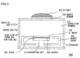
- Fig. 3 is a diagram showing the configuration of a deposition system according to the present embodiment.
- an Si wafer 206 is placed on a stage 268 which is provided with a heater 208.
- the stage 268 is supported by a supporting unit 214.
- Inlets for a reactive gas (H 2 O), a source gas of a metal compound, and a purge gas are formed in the system.
- An outlet for exhausting the gases out of the deposition chamber is formed in the right side of the system.
- a quartz cover 258 is provided in order to prevent gas components from adhering to the stage 268 and the supporting unit 214.
- An RTP unit 202 is installed over a quartz window 204 which is formed in a wall of the deposition chamber 216.
- the Si wafer 206 is maintained at a predetermined temperature by the heater 208 during deposition, and is heated rapidly by the RTP unit 202. That is, the heater 208 is a heat source for maintaining the Si wafer 206 at a predetermined deposition temperature, or the deposition temperature shown in Fig. 7B to be seen later, during deposition.
- the RTP unit 202 is a heat source for reaching the annealing temperature during thermal annealing.
- the RTP unit 202 may be a rapid thermal processing unit such as an infrared lamp, a laser annealing unit, and a flashing unit.
- the deposition chamber 216 is given a volume ratio significantly smaller than heretofore with respect to the flow rate of the purge gas.
- the interior of the deposition chamber 216 can thus be replaced with the cooling purge gas of high flow rate in a short time. Consequently, it becomes possible to lower the temperature inside the deposition chamber 216 sharply.
- the RTP unit 202 attached to the deposition system 200 allows a quick rise in temperature.
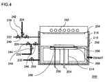
- Fig. 4 is a diagram showing the configuration of the deposition system 200 in more details.
- the configuration of the piping connected to the deposition chamber 216 is shown.
- Valves 238 and 240 are formed on a source gas supply pipe 222 for supplying the source gas of a metal compound thin film to the deposition chamber 216.
- the source gas supply pipe 222 is connected with a tank, a cylinder, or the like that contains the source gas.
- a purge gas supply pipe 224 communicating with the source gas supply pipe 222 is provided with a valve 242.
- the source gas may be the material of a high dielectric constant film (high-k material).
- a metal compound thin film having a high dielectric constant can be suitably formed on the surface of the Si wafer 206.
- Valves 244 and 246 are formed on a reactive gas supply pipe 226 for supplying the reactive gas (H 2 O) to the deposition chamber 216.
- the reactive gas supply pipe 226 is connected with a tank, a cylinder, or the like that contains the reactive gas.
- a purge gas supply pipe 228 communicating with the reactive gas supply pipe 226 is provided with a valve 248.
- a purge gas supply pipe 230 for introducing a large amount of cooling purge gas into the deposition chamber 216 is provided with a valve 250.
- the source gas supply pipe 222, the purge gas supply pipe 224, the reactive gas supply pipe 226, the purge gas supply pipe 228, and the purge gas supply pipe 230 may be made of any materials as long as they have resistance against the gas components flowing through the respective pipes and against the temperatures thereof.
- stainless steel pipes may be used.
- the valves 238 to 250 may be configured so that they are opened and closed under the control of a not-shown computer, for example.
- the walls of the deposition chamber 216 may be made of any material as long as it has resistance against heat, oxidants, and reductants. For example, stainless steel or other metals may be used.
- a heat insulating cover 210 may be arranged on the external walls of the deposition chamber 216.
- the heat insulating cover 210 may be made of glass wool, for example.
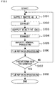
- a film material A is introduced from the source gas supply pipe 222 into the deposition chamber 216 and is supplied to the surface of the Si wafer 206 (S101).
- the valves 238 and 240 are open, and the valve 242 is closed.
- the material A is a metal compound.
- trimethyl aluminum (TMA) is used to form an aluminum oxide layer.
- ZrO 2 such a source gas as zirconium chloride (ZrCl 4 ) is selected and used as appropriate.
- HfO 2 such source gases as hafnium chloride (HfCl 4 ) and hafnium propoxide (Hf(iOPr) 4 ) may be used.
- source gases as hafnium chloride (HfCl 4 ) and hafnium propoxide (Hf(iOPr) 4 ) may be used.
- the temperature of the Si wafer 206 is adjusted by the heater 208.
- the temperature of the heater 208 is measured by a temperature measuring unit 256.
- the reactive gas is supplied from the reactive gas supply pipe 226 to the deposition chamber 216 (S103).
- the valves 244 and 246 are opened, and the valve 248 is closed.
- the examples of the reactive gas include H 2 O, O 3 , O 2 , N 2 O, NH 3 , and NO. Consequently, an oxygen atomic layer is formed on the atomic layer made of the material A.
- inactive gas purging is performed to exhaust the air (S104).
- the valve 244 is closed and the valve 248 is opened to introduce the purge gas from the purge gas supply pipe 228. Consequently, the reactive gas in the reactive gas supply pipe 226 can be removed suitably.
- thermal annealing is conducted for the sake of impurity removal processing and film reforming processing (S105, S106).
- This annealing is carried out inside the deposition chamber 216 where the foregoing steps S101 to S105 are performed. That is, the Si wafer 206 is thermally annealed simply without being taken out of the deposition chamber 216.
- the annealing temperature is set as appropriate according to the film materials etc. Typically, an appropriate temperature is selected from the range of 400°C to 1000°C.
- the heating temperature by the RTP unit 202 is adjusted based on the temperature measured by a radiation thermometer 254.
- the cycle consisting of the foregoing steps S101 to S106 is repeated to stack atomic layers. Subsequently, whether a predetermined thickness is reached or not is checked by a thickness measuring device (not shown) which is arranged on the deposition system 200 (S107). If the predetermined thickness is not reached (No at S107), the annealed Si wafer 206 is cooled rapidly to repeat the steps from S101.
- the rapid cooling of the deposition chamber 216 is effected by supplying the purge gas from the purge gas supply pipe 230 and exhausting the air from the outlet as well. This can cool the Si wafer 206 efficiently, so that the processing can be shifted from step S106 to S101 promptly.
- the atomic layer forming steps are ended. Then, annealing is performed for the sake of film refining processing (S108).
- Figs. 6A to 6D are diagrams schematically showing the process how atomic layers are stacked by the steps of Fig. 5.
- Fig. 6A shows the state after the execution of the steps S101 to S104 in Fig. 5.
- Metal atoms, oxygen atoms, and impurities are deposited on the substrate.
- Fig. 6B shows the state after the execution of the steps S105 and S106 in Fig. 5.
- the thermal annealing has removed the impurities from the film.
- Figs. 6C and 6D show the layer structure at respective stages after the foregoing steps are repeated.
- the thermal annealing provides the densified layer structure having little impurities as shown in Fig. 6D.
- Fig. 7A is a diagram showing the sequence of gas supply and wafer cooling. Initially, the source gas for material is supplied (sequence 1). Next, the reactive gas is supplied (sequence 2). Subsequently, annealing is performed for the sake of impurity removal and film densification (sequence 3). Then, the Si wafer 206 is cooled (sequence 4) to complete a single cycle of deposition steps. This cycle is performed a plurality of times to form the high dielectric constant thin film.
- Fig. 7B is a diagram showing the relationship among the cycle, the temperature of the Si wafer 206, and the gas flow rate.
- the numerals given to the deposition sequence of Fig. 7B correspond to those of Fig. 7A.
- the wafer temperature is maintained at a relatively low temperature. From the state after the completion of the deposition sequence 2, the temperature is increased rapidly by the RTP unit 202. The annealing is thus performed in the deposition sequence 3 (impurity removal, and densification). In the meantime, the wafer temperature is maintained high. The annealing is conducted by using an infrared lamp or laser annealing, and completed in a short time. Subsequently, the Si wafer 206 is cooled in the sequence 4.
- the deposition system 200 has the heater 208 and the RTP unit 202, it is possible to exercise high speed heating by the RTP unit 202 during annealing. Moreover, since the speed of introduction of the purge gas from the purge gas supply pipe 230 and the speed of exhaust of the purge gas from the outlet are significantly higher than in conventional systems, rapid cooling is also possible.
- the deposition system 200 it is possible to increase the temperature of the Si wafer 206 and cool the same rapidly. Then, the deposition and the annealing both can be achieved in the deposition chamber 216. This allows the process of performing deposition, annealing, and deposition again. Impurity contamination and film defects can thus be suppressed suitably, so that a thin film of favorable quality can be obtained stably.
- the deposition and the annealing can be performed at desired timing, it is possible to introduce different types of components into the thin film in a desired distribution.
- Figs. 8 and 9 are diagrams showing the configuration of a deposition system according to the present embodiment.
- Fig. 8 shows the state where a supporting unit 214 of the deposition system 260 is lifted.
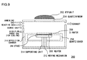
- Fig. 9 shows the state where the supporting unit 214 is lowered.
- the Si wafer 206 is placed on the supporting unit 214 which has a moving mechanism 212.
- the Si wafer 206 can thus be displaced in the height direction.
- the moving mechanism 212 may be configured to extend and contract the supporting unit 214 electrically.
- the moving mechanism 212 for changing the height of the supporting unit 214 according to an operation on a switch arranged outside the deposition chamber 216 may be formed inside the supporting unit 214.
- the deposition system 260 moves the Si wafer 206 upward to approach the RTP unit 202 as shown in Fig. 8.
- the Si wafer 206 is moved downward to draw apart from the RTP unit 202 as shown in Fig. 9.
- the interior of the chamber is purged by a large amount of purge gas introduced from the purge gas supply pipe 230.
- the outlet is formed in the upper part of the deposition chamber 216.
- the stage 268 and the gas supply channels have the same structures as in Fig. 6.
- the deposition system 260 is configured so as to be capable of adjusting the distance between the RTP unit 202 and the Si wafer 206.
- the outlet lies in the upper part of the deposition chamber 216. This allows prompt gas exchange and temperature adjustment, thereby achieving a structure better suited for rapid heating and rapid cooling.
- the distance between the RTP unit 202 and the Si wafer 206 is selected as appropriate according to such factors as the output of the RTP unit 202.
- Figs. 10 and 11 are diagrams showing the configuration of a deposition system according to the present embodiment.
- Fig. 10 shows the state where a supporting unit 214 of the deposition system 262 is lifted.
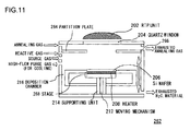
- Fig. 11 shows the state where the supporting unit 214 is lowered.
- the Si wafer 206 is placed on the supporting unit 214 which has a moving mechanism 212 as is the case with the deposition system 260 described in the second embodiment.
- the Si wafer 206 can thus be displaced in the height direction.
- a partition plate 264 is arranged at a position lower than the inlet of the annealing gas and higher than the inlets of the other gases.
- An outlet for exhausting the source gas and the reactive gas is formed in the lower part of the deposition chamber 216.
- an annealing gas outlet 266 for exhausting the purge gas or the annealing gas is formed in the upper part of the deposition chamber 216.
- the annealing gas outlet lies above the partition plate 264.
- the stage 268 and the gas supply channels have the same structures as in Fig. 4.
- the Si wafer 206 is moved by the moving mechanism 212 so that the quartz cover 258, the supporting unit 214, the Si wafer 206 on the supporting unit 214, and the partition plate 264 form a division wall together.
- the interior of the deposition chamber is intended for deposition alone.
- the Si wafer 206 must be taken out of the system and transported to a separate annealing system. Otherwise, even when the Si wafer 206 is not taken out of the deposition system 260, it must be transported to an annealing chamber separate from the deposition chamber.
- the partition plate 264 suitably forms a small chamber for annealing inside the deposition chamber 216. This configuration makes it possible to heat and cool the Si wafer 206 even more efficiently.
- the moving mechanism 212 is adjusted so that the sides of the partition plate 264 come into contact with the sides of the Si wafer 206 or the sides of the stage 268.
- the annealing gas is only supplied to and exhausted from the small chamber above the partition plate 264 while the flow of the annealing gas into the chamber below the partition plate 264 is blocked. Consequently, erosion of the inner walls of the deposition chamber 216, ascribable to contact of the annealing gas and the reactive gas inside the deposition chamber 216, can be suppressed suitably.
- a reductant gas NH 3 is selected as the annealing gas
- an oxidant gas H 2 O is selected as the reactive gas. If the two gases make contact with each other in the deposition chamber 216, they may promote erosion of the inner walls of the deposition chamber 216. This can be suppressed, however, by the provision of the partition plate 264. The same holds when an oxidant gas is selected as the annealing gas and a reductant gas is selected as the reactive gas. In addition, it is possible to suppress a drop in the degree of vacuum ascribable to the presence of the reactive gas (such as H 2 O) above the partition plate 264.
- the reactive gas such as H 2 O
- the small chamber above the partition plate 264 of the deposition chamber 216 can be reduced further in volume ratio with respect to the flow rate of the annealing gas.
- the annealing gas can thus be supplied more efficiently.
- thermal annealing is performed in this state, the Si wafer 206 can be heated even more rapidly since it lies closer to the RTP unit 202.
- the moving mechanism 212 is adjusted to position the Si wafer 206 below the inlet of the purge gas as shown in Fig. 11.
- the annealing gas outlet 266 arranged in the upper part of the deposition chamber 216 and the outlet formed in the lower part of the deposition chamber 216 both are used for exhaust. The cooling can thus be performed even more efficiently. This makes it possible to lower the temperature more sharply.
- the deposition system 262 is configured so that the sides of the partition plate 264 come into contact with the sides of the Si wafer 206 or the sides of the stage 268, there may be a predetermined clearance.
- Fig. 15 is a diagram for explaining a method of process management in the foregoing deposition systems.
- a process management unit 270 exercises schedule management on each individual process based on time information input from a clocking unit 272. This schedule management will now be described along the flowchart of Fig. 5, assuming the case of the deposition system 260 described in the second embodiment.
- a source gas control unit 276 controls the amount of the source gas to be supplied from the source gas supply pipe 222 (S101).
- the temperature of the heater 208 in the deposition process is controlled by a heater control unit 286.
- the source gas control unit 276 stops the supply of the source gas.
- An exhaust control unit 288 makes the deposition chamber 216 exhausted through the outlet (S102). After a lapse of a predetermined time, the exhaust is stopped.
- the reactive gas is supplied from the reactive gas supply pipe 226 for a predetermined time (S103).
- the supply of the reactive gas is controlled by a reactive gas control unit 278.
- the reactive gas control unit 278 stops the supply of the reactive gas.
- the exhaust control unit 288 makes the deposition chamber 216 exhausted (S104). After a lapse of a predetermined time, the exhaust is stopped.
- a moving mechanism control unit 274 operates the moving mechanism 212 for a predetermined time, so that the Si wafer 206 approaches the RTP unit 202.
- An RTP control unit 284 makes the RTP unit 202 start heating.
- An annealing gas control unit 280 supplies the annealing gas from the annealing gas supply pipe 218 to the deposition chamber 216 for a certain period of time (S105). After a lapse of a predetermined time, the heating of the RTP unit 202 and the supply of the annealing gas are stopped.
- a purge gas control unit 282 starts supplying the purge gas from the purge gas supply pipe 230, and the exhaust control unit 288 starts exhausting air from the outlet. The operations described above are repeated until a predetermined time. When the predetermined time has elapsed (Yes at S107), film refining processing is performed as in S105, thereby completing deposition.
- the process management shown in Fig. 15 may be scheduled such that the annealing gas is supplied at predetermined timing after the start of the heating by the RTP unit 202.
- Fig. 16 is a diagram for explaining another method of process management in the foregoing deposition systems.
- the moving mechanism control unit 274 controls the operation of the moving mechanism 212, it also controls the operations of the annealing gas control unit 280 and the RTP control unit 284 based on the position of the Si wafer 206 sensed by a substrate position sensing unit 290. Consequently, when the Si wafer 206 is moved to a predetermined position, the RTP control unit 284 makes the RTP unit 202 start heating, and the annealing gas control unit 280 starts the supply from the annealing gas supply pipe 218.
- the supply of the annealing gas may be scheduled so as to be started after a predetermined time since the heating of the RTP unit 202.
- the present embodiment relates to anther example of the deposition method that uses the deposition system 260 described in the second embodiment (Figs. 8 and 9).
- the present embodiment will deal with an example where annealing is performed in an atmosphere containing a nitrogen compound gas so that nitrogen is diffused into a metal compound layer.
- the RTP unit 202 shall be an infrared lamp.
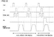
- Fig. 12 shows the gas supply and the temperature profile in the deposition process. This profile can be achieved, for example, by the method described in the fourth embodiment or the fifth embodiment.
- TMA trimethyl aluminum
- H 2 O gas the reactive gas
- thermal annealing is performed for the sake of impurity removal and film densification.
- the annealing temperature and time are 600°C to 1050°C and 1 to 600 sec, for example.
- the rate of temperature rise during annealing is 100°C/sec or higher.
- annealing processing is performed. That is, as shown in Fig. 12, NH 3 is supplied during annealing. Consequently, nitrogen is introduced and diffused into the layer.
- the annealing conditions here are the same as described above.
- the crystallization temperature of the film increases for improved film quality.
- the chemical stability improves as well.
- the resulting film has such characteristics as a lower barrier against electron and a propensity to trapping electron.
- nitrogen can be introduced into the metal oxide film with a certain distribution of nitrogen concentration to form high-nitrogen and low-nitrogen regions, then it becomes possible to achieve excellent device performance previously unavailable. Since the method of the present embodiment allows precise control on such a distribution of nitrogen concentration, it can be suitably used for device manufacturing steps.
- the deposition systems 200 and 262 may also be used.
- the sixth embodiment has dealt with the case where annealing is performed each time an atomic layer is formed.
- the present embodiment adopts a method of performing annealing after a plurality of atomic layers are stacked.
- the present embodiment will deal with the case where Al 2 O 3 and AlON are layered in this order on a silicon substrate by ALD.
- the deposition system 260 described in the second embodiment (Figs. 8 and 9) is used, for example.
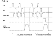
- Fig. 13 shows the gas supply and the temperature profile in the deposition process. This profile can be achieved, for example, by the method described in the fourth embodiment or the fifth embodiment.
- TMA trimethyl aluminum
- H 2 O gas the reactive gas
- Both aluminum and oxygen are deposited at temperatures of around 150°C to 450°C.
- steps A and B are performed for two to five cycles, thereby forming an Al 2 O 3 layer.
- thermal annealing is performed for the sake of impurity removal and film densification.
- the annealing temperature and time are 600°C to 1050°C and 1 to 600 sec, for example.
- the rate of temperature rise during annealing is 100°C/sec or higher (step C).
- steps A and B are performed for two to five cycles to form an Al 2 O 3 layer, followed by the thermal annealing of step C.
- a nitrogen compound gas is introduced into the deposition chamber (step D).
- ammonia is introduced.
- nitrogen is introduced into the aluminum oxide layer, thereby forming an AlON layer.
- a high dielectric constant thin film having Al 2 O 3 and AlON layered in this order can thus be formed by using the process described above.
- the deposition systems 200 and 262 may also be used.
- annealing is performed after the formation of several atomic layers.
- a high dielectric constant material film of favorable quality can thus be obtained through the simple process.
Landscapes
- Chemical & Material Sciences (AREA)
- General Chemical & Material Sciences (AREA)
- Chemical Kinetics & Catalysis (AREA)
- Engineering & Computer Science (AREA)
- Materials Engineering (AREA)
- Mechanical Engineering (AREA)
- Metallurgy (AREA)
- Organic Chemistry (AREA)
- Chemical Vapour Deposition (AREA)
- Internal Circuitry In Semiconductor Integrated Circuit Devices (AREA)
Applications Claiming Priority (3)
| Application Number | Priority Date | Filing Date | Title |
|---|---|---|---|
| JP2003083692 | 2003-03-25 | ||
| JP2003083692A JP4257576B2 (ja) | 2003-03-25 | 2003-03-25 | 成膜装置 |
| PCT/JP2004/004076 WO2004086481A1 (ja) | 2003-03-25 | 2004-03-24 | 成膜装置 |
Publications (2)
| Publication Number | Publication Date |
|---|---|
| EP1608006A1 true EP1608006A1 (de) | 2005-12-21 |
| EP1608006A4 EP1608006A4 (de) | 2007-01-31 |
Family
ID=33094969
Family Applications (1)
| Application Number | Title | Priority Date | Filing Date |
|---|---|---|---|
| EP04722958A Withdrawn EP1608006A4 (de) | 2003-03-25 | 2004-03-24 | Filmerzeugungsvorrichtung |
Country Status (6)
| Country | Link |
|---|---|
| US (1) | US7387686B2 (de) |
| EP (1) | EP1608006A4 (de) |
| JP (1) | JP4257576B2 (de) |
| KR (1) | KR20050109601A (de) |
| TW (1) | TW200420747A (de) |
| WO (1) | WO2004086481A1 (de) |
Cited By (4)
| Publication number | Priority date | Publication date | Assignee | Title |
|---|---|---|---|---|
| EP1728894A1 (de) * | 2005-06-01 | 2006-12-06 | Interuniversitair Microelektronica Centrum ( Imec) | Beschichtungsverfahren mit atomaren Schichten (ald) zum Erzeugen einer Schicht hoher Qualität |
| WO2007042797A1 (en) * | 2005-10-11 | 2007-04-19 | Aviza Technology Limited | Positive displacement pumping chamber |
| EP1790758A1 (de) * | 2005-11-25 | 2007-05-30 | Interuniversitair Microelektronica Centrum ( Imec) | Beschichtungsverfahren mit atomaren Schichten (ald) zum Erzeugen einer Schicht hoher Qualität |
| EP1674592A3 (de) * | 2004-12-22 | 2009-04-22 | Canon Anelva Corporation | Beschichtungsanlage mit mehreren Kammern |
Families Citing this family (37)
| Publication number | Priority date | Publication date | Assignee | Title |
|---|---|---|---|---|
| JP4590402B2 (ja) * | 2004-04-30 | 2010-12-01 | 株式会社荏原製作所 | 基板の処理装置 |
| US7648578B1 (en) * | 2004-06-15 | 2010-01-19 | Hitachi Kokusai Electric Inc. | Substrate processing apparatus, and method for manufacturing semiconductor device |
| KR101332739B1 (ko) * | 2005-01-18 | 2013-11-25 | 에이에스엠 아메리카, 인코포레이티드 | 박막 성장용 반응 시스템 |
| US7402778B2 (en) * | 2005-04-29 | 2008-07-22 | Asm Assembly Automation Ltd. | Oven for controlled heating of compounds at varying temperatures |
| WO2007040057A1 (ja) * | 2005-10-04 | 2007-04-12 | Nec Corporation | 半導体装置 |
| JP4946145B2 (ja) * | 2006-04-13 | 2012-06-06 | 富士通セミコンダクター株式会社 | 強誘電体メモリの製造方法 |
| KR100872799B1 (ko) * | 2007-09-11 | 2008-12-09 | 포항공과대학교 산학협력단 | 플라스마 원자층 증착법을 이용한 반도체 콘택트용 금속실리사이드 제조방법 |
| JP4905315B2 (ja) * | 2007-10-19 | 2012-03-28 | 東京エレクトロン株式会社 | 半導体製造装置、半導体製造方法及び記憶媒体 |
| KR101111494B1 (ko) * | 2008-02-18 | 2012-02-23 | 미쯔이 죠센 가부시키가이샤 | 원자층 성장 장치 및 원자층 성장 방법 |
| JP2009209435A (ja) * | 2008-03-06 | 2009-09-17 | Mitsui Eng & Shipbuild Co Ltd | 原子層成膜装置 |
| JP5292032B2 (ja) * | 2008-09-16 | 2013-09-18 | 東京エレクトロン株式会社 | 重合膜の成膜方法および成膜装置 |
| US9328417B2 (en) * | 2008-11-01 | 2016-05-03 | Ultratech, Inc. | System and method for thin film deposition |
| US9175388B2 (en) * | 2008-11-01 | 2015-11-03 | Ultratech, Inc. | Reaction chamber with removable liner |
| JP4523661B1 (ja) * | 2009-03-10 | 2010-08-11 | 三井造船株式会社 | 原子層堆積装置及び薄膜形成方法 |
| JP2010278319A (ja) * | 2009-05-29 | 2010-12-09 | Renesas Electronics Corp | 半導体装置およびその製造方法 |
| US9127360B2 (en) * | 2009-10-05 | 2015-09-08 | Applied Materials, Inc. | Epitaxial chamber with cross flow |
| US20110256682A1 (en) * | 2010-04-15 | 2011-10-20 | Taiwan Semiconductor Manufacturing Company, Ltd. | Multiple Deposition, Multiple Treatment Dielectric Layer For A Semiconductor Device |
| KR101147727B1 (ko) * | 2010-08-02 | 2012-05-25 | 주식회사 유진테크 | 사이클릭 박막 증착 방법 |
| US9512520B2 (en) * | 2011-04-25 | 2016-12-06 | Applied Materials, Inc. | Semiconductor substrate processing system |
| CN104053626B (zh) * | 2011-10-28 | 2017-06-30 | 意法半导体股份有限公司 | 用于制造针对氢氟酸蚀刻的保护层的方法、设置有该保护层的半导体器件及制造该半导体器件的方法 |
| GB201206096D0 (en) * | 2012-04-05 | 2012-05-16 | Dyson Technology Ltd | Atomic layer deposition |
| WO2013162972A1 (en) * | 2012-04-25 | 2013-10-31 | Applied Materials, Inc. | Process chamber having separate process gas and purge gas regions |
| JP2014055342A (ja) * | 2012-09-14 | 2014-03-27 | Hitachi High-Technologies Corp | 成膜装置 |
| WO2014097280A1 (en) * | 2012-12-21 | 2014-06-26 | Prasad Narhar Gadgil | Methods of low temperature deposition of ceramic thin films |
| JP6101083B2 (ja) * | 2013-01-16 | 2017-03-22 | 東京エレクトロン株式会社 | 成膜方法及び成膜装置 |
| KR102337670B1 (ko) * | 2015-03-30 | 2021-12-09 | 삼성디스플레이 주식회사 | 박막 증착 장치 및 이를 이용한 박막 증착 방법 |
| US10797238B2 (en) | 2016-01-26 | 2020-10-06 | Arm Ltd. | Fabricating correlated electron material (CEM) devices |
| JP2017152574A (ja) * | 2016-02-25 | 2017-08-31 | 京セラ株式会社 | 光電変換膜および光電変換装置 |
| KR101816861B1 (ko) * | 2016-10-21 | 2018-01-10 | (주)제이하라 | 플라즈마 표면 처리장치 |
| US11447861B2 (en) * | 2016-12-15 | 2022-09-20 | Asm Ip Holding B.V. | Sequential infiltration synthesis apparatus and a method of forming a patterned structure |
| US10872804B2 (en) | 2017-11-03 | 2020-12-22 | Asm Ip Holding B.V. | Apparatus and methods for isolating a reaction chamber from a loading chamber resulting in reduced contamination |
| US10872803B2 (en) | 2017-11-03 | 2020-12-22 | Asm Ip Holding B.V. | Apparatus and methods for isolating a reaction chamber from a loading chamber resulting in reduced contamination |
| JP6637095B2 (ja) * | 2018-03-22 | 2020-01-29 | プラサド ナーハー ガジル | セラミック薄膜の低温堆積方法 |
| US10573532B2 (en) * | 2018-06-15 | 2020-02-25 | Mattson Technology, Inc. | Method for processing a workpiece using a multi-cycle thermal treatment process |
| CA3043564C (fr) | 2019-05-15 | 2026-02-10 | Safran | Procede de formation d'une couche d'alumine a la surface d'un substrat metallique |
| CN114107947A (zh) * | 2020-08-28 | 2022-03-01 | 昆山微电子技术研究院 | 原子层沉积设备 |
| IT202100022511A1 (it) | 2021-08-30 | 2023-03-02 | St Microelectronics Srl | Procedimento di fabbricazione di un sistema integrato includente un sensore di pressione capacitivo e un sensore inerziale, e sistema integrato |
Family Cites Families (18)
| Publication number | Priority date | Publication date | Assignee | Title |
|---|---|---|---|---|
| NL8602356A (nl) | 1985-10-07 | 1987-05-04 | Epsilon Ltd Partnership | Inrichting en werkwijze voor een axiaal symmetrische reactor voor het chemische uit damp neerslaan. |
| US5245171A (en) * | 1990-07-27 | 1993-09-14 | Harvey Fox | Mailing article with audible message generator |
| DE69130205T2 (de) * | 1990-12-25 | 1999-03-25 | Ngk Insulators, Ltd., Nagoya, Aichi | Heizungsapparat für eine Halbleiterscheibe und Verfahren zum Herstellen desselben |
| US5387557A (en) * | 1991-10-23 | 1995-02-07 | F. T. L. Co., Ltd. | Method for manufacturing semiconductor devices using heat-treatment vertical reactor with temperature zones |
| US5444217A (en) * | 1993-01-21 | 1995-08-22 | Moore Epitaxial Inc. | Rapid thermal processing apparatus for processing semiconductor wafers |
| JP2642858B2 (ja) * | 1993-12-20 | 1997-08-20 | 日本碍子株式会社 | セラミックスヒーター及び加熱装置 |
| US5730801A (en) * | 1994-08-23 | 1998-03-24 | Applied Materials, Inc. | Compartnetalized substrate processing chamber |
| US6251758B1 (en) * | 1994-11-14 | 2001-06-26 | Applied Materials, Inc. | Construction of a film on a semiconductor wafer |
| JPH08288283A (ja) * | 1995-04-14 | 1996-11-01 | Ricoh Co Ltd | シリコン酸化膜形成方法およびシリコン酸化膜形成装置 |
| US6156149A (en) * | 1997-05-07 | 2000-12-05 | Applied Materials, Inc. | In situ deposition of a dielectric oxide layer and anti-reflective coating |
| US6077764A (en) * | 1997-04-21 | 2000-06-20 | Applied Materials, Inc. | Process for depositing high deposition rate halogen-doped silicon oxide layer |
| KR100319494B1 (ko) * | 1999-07-15 | 2002-01-09 | 김용일 | 원자층 에피택시 공정을 위한 반도체 박막 증착장치 |
| TW515032B (en) | 1999-10-06 | 2002-12-21 | Samsung Electronics Co Ltd | Method of forming thin film using atomic layer deposition method |
| JP4817210B2 (ja) | 2000-01-06 | 2011-11-16 | 東京エレクトロン株式会社 | 成膜装置および成膜方法 |
| DE10296448T5 (de) | 2001-03-20 | 2004-04-15 | Mattson Technology Inc., Fremont | Verfahren zum Abscheiden einer Schicht mit einer verhältnismässig hohen Dielektrizitätskonstante auf ein Substrat |
| JP2002314072A (ja) | 2001-04-19 | 2002-10-25 | Nec Corp | 高誘電体薄膜を備えた半導体装置及びその製造方法並びに誘電体膜の成膜装置 |
| JP3896395B2 (ja) * | 2001-06-20 | 2007-03-22 | 大日本スクリーン製造株式会社 | 熱処理装置 |
| US6753506B2 (en) * | 2001-08-23 | 2004-06-22 | Axcelis Technologies | System and method of fast ambient switching for rapid thermal processing |
-
2003
- 2003-03-25 JP JP2003083692A patent/JP4257576B2/ja not_active Expired - Lifetime
-
2004
- 2004-03-24 US US10/550,753 patent/US7387686B2/en not_active Expired - Fee Related
- 2004-03-24 TW TW093108012A patent/TW200420747A/zh unknown
- 2004-03-24 EP EP04722958A patent/EP1608006A4/de not_active Withdrawn
- 2004-03-24 KR KR1020057017890A patent/KR20050109601A/ko not_active Withdrawn
- 2004-03-24 WO PCT/JP2004/004076 patent/WO2004086481A1/ja not_active Ceased
Cited By (4)
| Publication number | Priority date | Publication date | Assignee | Title |
|---|---|---|---|---|
| EP1674592A3 (de) * | 2004-12-22 | 2009-04-22 | Canon Anelva Corporation | Beschichtungsanlage mit mehreren Kammern |
| EP1728894A1 (de) * | 2005-06-01 | 2006-12-06 | Interuniversitair Microelektronica Centrum ( Imec) | Beschichtungsverfahren mit atomaren Schichten (ald) zum Erzeugen einer Schicht hoher Qualität |
| WO2007042797A1 (en) * | 2005-10-11 | 2007-04-19 | Aviza Technology Limited | Positive displacement pumping chamber |
| EP1790758A1 (de) * | 2005-11-25 | 2007-05-30 | Interuniversitair Microelektronica Centrum ( Imec) | Beschichtungsverfahren mit atomaren Schichten (ald) zum Erzeugen einer Schicht hoher Qualität |
Also Published As
| Publication number | Publication date |
|---|---|
| EP1608006A4 (de) | 2007-01-31 |
| US7387686B2 (en) | 2008-06-17 |
| KR20050109601A (ko) | 2005-11-21 |
| WO2004086481A1 (ja) | 2004-10-07 |
| US20060180082A1 (en) | 2006-08-17 |
| JP4257576B2 (ja) | 2009-04-22 |
| TW200420747A (en) | 2004-10-16 |
| JP2004296537A (ja) | 2004-10-21 |
Similar Documents
| Publication | Publication Date | Title |
|---|---|---|
| US7387686B2 (en) | Film formation apparatus | |
| US9653301B2 (en) | Semiconductor device having electrode made of high work function material, method and apparatus for manufacturing the same | |
| TWI420597B (zh) | 用以形成掺雜有金屬之含矽絕緣膜的膜形成方法與膜形成設備 | |
| US7816200B2 (en) | Hardware set for growth of high k and capping material films | |
| US20110003482A1 (en) | Method of manufacturing semiconductor device and substrate processing system | |
| US9190281B2 (en) | Method of manufacturing semiconductor device | |
| WO2007019449A1 (en) | In-situ atomic layer deposition | |
| JP2008311631A (ja) | 化学気相堆積プロセスを用いて高k誘電物質を堆積させる方法 | |
| TW202247469A (zh) | 以偶極膜工程化的mosfet閘極 | |
| KR20180073453A (ko) | 성막 장치 및 성막 방법 | |
| US20110151660A1 (en) | Method of manufacturing semiconductor device, method of processing substrate and substrate processing apparatus | |
| US11306847B2 (en) | Valve device, processing apparatus, and control method | |
| WO2012106612A2 (en) | In-situ hydroxylation system | |
| JP4007044B2 (ja) | 原子層蒸着法を用いた薄膜形成方法 | |
| JP4735601B2 (ja) | 原子層蒸着法を用いた薄膜形成方法 | |
| KR20150125674A (ko) | SiOC를 포함하는 막의 촉매적 원자층 증착 | |
| KR102857454B1 (ko) | 비정질 실리콘-기반 스캐빈징 및 밀봉 eot | |
| CN106978599A (zh) | 原子层沉积设备 | |
| US20130087099A1 (en) | In-Situ Hydroxylation Apparatus | |
| US11018009B2 (en) | Tuning work function of p-metal work function films through vapor deposition | |
| CN116918070A (zh) | 具有偶极膜的mosfet栅极工程 | |
| EP3413333B1 (de) | Bildung von metalloxidschicht | |
| CN115136284A (zh) | 基板处理装置、半导体装置的制造方法、存储介质以及内管 | |
| KR102876047B1 (ko) | 성막 방법, 반도체 장치의 제조 방법, 처리 시스템 및 커패시터 | |
| US20240332014A1 (en) | Doping by molecular layer deposition |
Legal Events
| Date | Code | Title | Description |
|---|---|---|---|
| PUAI | Public reference made under article 153(3) epc to a published international application that has entered the european phase |
Free format text: ORIGINAL CODE: 0009012 |
|
| 17P | Request for examination filed |
Effective date: 20050926 |
|
| AK | Designated contracting states |
Kind code of ref document: A1 Designated state(s): AT BE BG CH CY CZ DE DK EE ES FI FR GB GR HU IE IT LI LU MC NL PL PT RO SE SI SK TR |
|
| AX | Request for extension of the european patent |
Extension state: AL LT LV MK |
|
| DAX | Request for extension of the european patent (deleted) | ||
| RBV | Designated contracting states (corrected) |
Designated state(s): BE DE FI FR |
|
| A4 | Supplementary search report drawn up and despatched |
Effective date: 20070102 |
|
| RAP1 | Party data changed (applicant data changed or rights of an application transferred) |
Owner name: HORIBA, LTD. Owner name: RENESAS TECHNOLOGY CORP. Owner name: ROHM CO., LTD. |
|
| STAA | Information on the status of an ep patent application or granted ep patent |
Free format text: STATUS: THE APPLICATION HAS BEEN WITHDRAWN |
|
| 18W | Application withdrawn |
Effective date: 20090407 |