EP1597908B1 - Apparatus in a tv receiver automatically detecting the type of keyboard attached thereto - Google Patents
Apparatus in a tv receiver automatically detecting the type of keyboard attached thereto Download PDFInfo
- Publication number
- EP1597908B1 EP1597908B1 EP04710672A EP04710672A EP1597908B1 EP 1597908 B1 EP1597908 B1 EP 1597908B1 EP 04710672 A EP04710672 A EP 04710672A EP 04710672 A EP04710672 A EP 04710672A EP 1597908 B1 EP1597908 B1 EP 1597908B1
- Authority
- EP
- European Patent Office
- Prior art keywords
- keyboard
- front panel
- controller
- voltage
- operational
- Prior art date
- Legal status (The legal status is an assumption and is not a legal conclusion. Google has not performed a legal analysis and makes no representation as to the accuracy of the status listed.)
- Expired - Lifetime
Links
- 230000004913 activation Effects 0.000 claims description 25
- 238000000034 method Methods 0.000 claims description 14
- 230000008878 coupling Effects 0.000 claims description 4
- 238000010168 coupling process Methods 0.000 claims description 4
- 238000005859 coupling reaction Methods 0.000 claims description 4
- 239000004065 semiconductor Substances 0.000 claims description 3
- 229910044991 metal oxide Inorganic materials 0.000 claims 2
- 150000004706 metal oxides Chemical class 0.000 claims 2
- 230000002457 bidirectional effect Effects 0.000 claims 1
- 239000004020 conductor Substances 0.000 claims 1
- 230000008569 process Effects 0.000 description 6
- 230000008859 change Effects 0.000 description 4
- 239000000872 buffer Substances 0.000 description 3
- 230000001105 regulatory effect Effects 0.000 description 3
- 239000003990 capacitor Substances 0.000 description 2
- 230000000994 depressogenic effect Effects 0.000 description 2
- 230000000694 effects Effects 0.000 description 2
- 230000003213 activating effect Effects 0.000 description 1
- 238000013459 approach Methods 0.000 description 1
- 230000008901 benefit Effects 0.000 description 1
- 230000003247 decreasing effect Effects 0.000 description 1
- 230000001934 delay Effects 0.000 description 1
- 230000001419 dependent effect Effects 0.000 description 1
- 238000013461 design Methods 0.000 description 1
- 238000012544 monitoring process Methods 0.000 description 1
- 238000012545 processing Methods 0.000 description 1
- 230000005855 radiation Effects 0.000 description 1
Images


Classifications
-
- H—ELECTRICITY
- H04—ELECTRIC COMMUNICATION TECHNIQUE
- H04N—PICTORIAL COMMUNICATION, e.g. TELEVISION
- H04N5/00—Details of television systems
- H04N5/44—Receiver circuitry for the reception of television signals according to analogue transmission standards
-
- H—ELECTRICITY
- H04—ELECTRIC COMMUNICATION TECHNIQUE
- H04N—PICTORIAL COMMUNICATION, e.g. TELEVISION
- H04N5/00—Details of television systems
- H04N5/63—Generation or supply of power specially adapted for television receivers
Definitions
- This invention relates to the field of television receivers, and, more particularly, to apparatus in a television receiver for automatically detecting the type of keyboard attached to the television receiver.
- Most television (TV) apparatus includes a front panel keyboard for a user to operate the television apparatus.
- a television apparatus normally includes a controller for receiving, detecting, identifying key activation signals from the front panel keyboard, and operating the television according to the function of the key being activated, for example, by pressing or touching.
- the front panel keyboard may include a top light or a backlight for lighting the keyboard when the television apparatus has been powered on.
- the front panel keyboard may have a power LED to indicate that the TV is "on".
- the top light, backlight, or power LED is turned on normally by a signal, such as a voltage, sent by the controller to the top light, backlight or power LED.
- TV receivers having a display screen commonly called TV sets
- TV receivers without a display screen such as VCRs, VCPs (videocassette players), set-top boxes (such as cable boxes and satellite receivers), and Videodisk players.
- the front panel keyboard In assembling a television apparatus, the front panel keyboard normally is one of the last few tasks to be installed. However, there are generally two different types of front panel keyboard to be supported: one with negative operational logic and the other with positive operational logic. In a keyboard with negative operation logic, the controller should provide a keyboard operational voltage to the keyboard. This type of keyboard normally uses momentary contact switches. By contrast, in a keyboard with positive operational logic, the keyboard provides its own keyboard operational voltage and the controller does not have to provide one for the keyboard. In general, front panel keyboards with positive operational logic have pull-down resistors on keyboard sense lines to set a logic zero condition on the keyboard inputs until a logic one is provided by a contact closure on the keyboard. A keyboard employing positive logic may have touch buttons, which use a capacitance change near a button indicating that the button has been pressed (activated).
- EP0773674 discloses a video signal processing system producing an output signal suitable for producing a closed caption display and is responsive to a freeze command from a user for modifying generation of the output signal such that the content of the closed caption region of the display does not change.
- the system provides for user selection of various freeze modes including one in which just the caption region of the display is frozen and another in which both the caption and video regions of the display are frozen.
- US6011328 discloses an electric power lockout apparatus including an input terminal for electrically coupling the apparatus to an electric power source and an output terminal for electrically coupling the apparatus to a device requiring electric power.
- the electric power lockout apparatus also has a switch that is electrically coupled between the input terminal and the output terminal.
- the switch is capable of assuming an open state wherein the input terminal is electrically isolated from the output terminal and the switch is capable of assuming a closed state wherein the input terminal is electrically coupled to the output terminal.
- the electric power lockout apparatus further has a first lock which controls operation of the switch so that the switch cannot assume the closed state unless the first lock is unlocked at least momentarily.
- the electric power lockout apparatus also has a locking structure to secure the electric power lockout apparatus to the power cord of an appliance.
- US5036261 discloses a standby/run power supply and control circuit for a television apparatus comprising first and second sources of DC voltage, one of which is unswitched and available during a standby mode of operation and the other one of which is switched and available only during a run mode operation.
- a voltage regulator has an input coupled to both DC sources and has an output for supplying a regulated DC voltage at a first power level during the standby mode and at a second power level during the run mode.
- a first control circuit is coupled to the regulated voltage output and operable in both the standby and run modes.
- a second control circuit is interconnected with the first control circuit and is also coupled to the regulated voltage output but is operable only during the run mode.
- the first control circuit is energised by the first source in the standby modeand both first and second control circuits are energised by the second source at a common voltage level in the run mode. Reliance on standby power during the run mode is minimized. The time during which power is available to a microprocessor for effecting controlled shutdown during AC power interruption is maximised.
- the present invention is a television apparatus according to claim 1 and a method for detecting a type of operational logic of a front panel keyboard of a television apparatus according to claim 20.
- a television apparatus includes a front panel keyboard having first and second keys, and a controller for detecting a type of operational logic of the front panel keyboard.
- the controller applies a keyboard operational voltage to the front panel keyboard according to the detected type of operational logic.
- the controller determines that the type of operational logic is negative, the controller applies the keyboard operational voltage to the front panel keyboard. Otherwise, if the controller determines that the type of operational logic is positive, the controller applies no keyboard operational voltage to the front panel keyboard.
- Each key when activated by a user sends a key activation signal to the controller through a keyboard sense line.
- the front panel keyboard includes a light and the controller applies a voltage to turn on the light through a light control line.
- the controller detects the type of operational logic of the front panel by detecting an identification voltage applied by the front panel keyboard to a first control line.
- the first control line is the light control line. If the identification voltage is detected, the controller determines that the type of operational logic of the front panel keyboard is positive and does not apply the keyboard operational voltage to the keyboard sense line.
- Front panel keyboards with positive operational logic typically have pull-down resistors on the keyboard lines to set a logic zero condition on the keyboard inputs until a logic one is provided by a contact closure on the keyboard. If the identification voltage is not detected, the controller determines that the type of operational logic of the front panel keyboard is negative and applies the keyboard operational voltage to the keyboard line through a keyboard control line.
- a front panel keyboard using positive logic includes first and second keys sharing a keyboard sense line coupled to the controller of the television apparatus for the controller to detect that one of the two keys has been activated; an inverter to invert a key drive signal from the controller, wherein the controller sends the key drive signal to detect whether the activation signal is coming from the first key or the second key; and an AND gate for generating the key activation signal from the second key and the inverted key drive signal.
- FIG. 1 illustrates a portion of a television apparatus 100 according to the principles of the invention.
- the television apparatus 100 includes a controller 110 and a front panel keyboard 170 sending user inputs to the controller 110.
- the controller 110 Upon receiving a user input, the controller 110 operates the television apparatus 100 according to the function specified in the user signal. Only those portions of the television apparatus necessary for understanding the present invention are included in FIG. 1 . Others are omitted for simplicity.
- the television apparatus 100 should also include a tuner, a display driver, and loudspeaker drivers.
- the front panel keyboard 170 normally includes an array of keys.
- the array of keys and other components of the front panel keyboard 170 are not shown in FIG. 1 , but these components will be illustrated in FIGs. 2 and 3 .
- the front panel keyboard 170 sends a corresponding user signal in the form of a key activation signal to the controller 110 through keyboard sense lines KS 1-KS4.
- the number of the keyboard sense lines may be different, depending on the number of keys to be supported in the front panel keyboard 170.
- each of the keyboard sense lines KS 1-KS4 is shared by more than one key, and the controller 110 should scan the front panel keyboard 170 by monitoring the state of a keyboard sense line having the key activation signal, while sending a keyboard drive signal to the front panel keyboard 170 through the keyboard drive line KD in order to determine exactly which key has been activated, as will be discussed in more detail in describing illustrative keyboards in FIGs. 2 and 3 .
- the keyboard drive line KD illustratively includes a resistor R13 having a protection resistance (for example, one kilo-ohm).
- the front panel keyboard 170 may also include a light for a user to more clearly see the keys on the front panel keyboard 170, or it may include a backlight to illuminate the keys from the back side, or it may include a power LED to indicate when the TV is turned "on".
- the controller 110 uses the example of a top light over the buttons, the controller 110 turns on the light by applying a light control voltage through a light control line 150.
- the front panel keyboard 170 also applies an identification signal, such as an identification voltage, to the light control line 150, so that the controller 110 can determine a type of operational logic of the front panel keyboard 170 from the identification signal.
- the identification signal of course, can be sent through a different control line. However, sharing the light control line reduces the cost of the television apparatus.
- the controller 110 includes a microprocessor 115 and a FPGA (field programmable gate array) 120.
- the microprocessor 115 reads and writes to the FPGA 120 through a local bus 116, but other bus schemes like the I 2 C bus could be used.
- the term "microprocessor” represents various devices including, but not limited to, microprocessors, microcomputers, microcontrollers and controllers.
- the FPGA 120 includes a keyboard register 121, which includes seven bits 1-7, of which bits 1-4 and 7 are read-only and bits 5 and 6 are writeable by the microprocessor 115.
- the FPGA 120 includes key input buffers (receivers) 131-134 respectively coupled to the key sense lines KS1-KS4 for receiving key activation signals, converting them into logic values, and saving the respective logic values into respective bits 1-4 in the keyboard control register 121. For example, if a received key activation signal is greater than a first threshold, it is saved as logic one in the corresponding bit, and if the received key activation signal is less than a second threshold, it is saved as a logic zero.
- the first threshold should be set to 2.0 volts and the second threshold should be set to 1.0 volt.
- the second threshold should be set to 0.8 volt.
- the FPGA 120 includes a transceiver 140 coupled to the light control line 150.
- the transceiver 140 includes a receiver 136 coupled to bit 7 of the keyboard register 121, for receiving the identification signal from the front panel keyboard 170, and a transmitter 137 coupled to a register 138 for applying a voltage through the transmitter 137 to the light control line 150 for turning on a light in the front panel keyboard 170.
- the identification signal may be a voltage signal.
- the microprocessor 115 determines that a type of operational logic of the front panel keyboard is positive.
- the microprocessor 115 determines that the type of operational logic of the front panel keyboard 170 is negative.
- a front panel keyboard with positive operational logic supplies its own operational voltage for operating the keyboard and resistive pull-downs to set the logic state to zero when no keys are depressed; whereas, a keyboard with negative operational logic requires the controller to supply the keyboard operational voltage.
- Control line 150 illustratively includes a protection resistor R16 having a resistance of, for example, one kilo-ohm. The resistance of the protection resister R16 can be different as long as the resulting voltage is sufficient to turn on the light on the front panel keyboard as discussed in more detail later.
- An optional capacitor (not shown), for example, having a capacitance of 1000 picofarads, is added, such that the capacitor and R16 form a RC circuit to roll off any edges from the clock used in the FPGA 120.
- the RC circuit may prevent a cable assembly attached to the FPGA 120 from radiating these clock harmonics, for satisfying FCC "open field radiation" level specifications.
- the FPGA 120 includes a switch 130, which is controlled by bit 6 of the keyboard register 121.
- the switch consists of a general purpose output pin having the capability of either applying a positive voltage to the keyboard control line 145 or setting the voltage on the control line 145 to zero.
- register bit 6 is a logic zero which sets switch 130 to output a positive voltage, for example, of approximately 3.3V.
- This output provides a keyboard operational voltage source for keyboard control line 145, which provides the pull-up voltage for keyboard sense lines KS 1-KS4.
- register bit 6 is a logic one and switch 130 provides zero volts to the keyboard control line 145.
- control line provides a resistive path to ground for the KS 1-KS4 lines through R5-R8.
- the microprocessor 115 detects that the type of operational logic of the front panel keyboard 170 is positive, i.e., bit 7 has a logic value of one, the microprocessor 115 sets bit 6 to one, which operates the switch 130 in such a way that the keyboard operational voltage source is not sourced from the keyboard control line 145.
- the keyboard operational voltage is a voltage source of 3.3 volts
- the switch 130 includes a standard CMOS driver, which includes a P-Channel MOS pull-up transistor 510 and an N-MOS pull-down transistor 520, as shown in FIG. 5 .
- the pull-up transistor 510 serves as a normally closed switch and in this application is always in conductive state, essentially functioning as a resistor.
- the drain electrode of the pull-up transistor 510 serves as the source for the keyboard operational voltage, the drain electrode is coupled to a drain electrode of the N-MOS pull-down transistor 520.
- the output of switch 130 is a voltage source of approximately 3.3V. This voltage source then drives keyboard control line 145 and provides a positive pull-up voltage to KS1-KS4 through the keyboard pull-up resistors R5-R8.
- the N-MOS pull-down transistor 520 serves as a normally opened switch controllable by the state of bit 6. If bit 6 has a logic value of zero, the N-MOS pull-down transistor 520 is in a non-conductive state. On the other hand, if bit 6 has a logic value of one, the N-MOS pull-down transistor 520 is in a conductive state, which exhibits a very low resistance as compared to the resistance exhibited by the pull-up transistor 510. As stated above, the drain electrode of the N-MOS pull-down transistor 520 is coupled to the drain electrode of the pull-up transistor 510 for providing the output of the switch 130. The source electrode of the N-MOS pull-down transistor 520 is coupled to ground, and the gate electrode is coupled to bit 6, so that state of bit 6 controls the state of the N-MOS pull-down transistor 520 as described below.
- the N-MOS pull-down transistor 520 is in a nonconductive (off) state and the operational voltage source is coupled to the keyboard control line 145.
- the microprocessor 115 detects that the type of operational logic of the front panel keyboard 170 is positive, the microprocessor 115 sets bit 6 to a logic one, which applies a control voltage to the gate electrode of the N-MOS pull-down transistor 520, causing the N-MOS pull-down transistor 520 in a conductive state.
- the voltage at the drain electrode of the N-MOS pull-down transistor 520 is low, equivalent to grounding the keyboard control line 145.
- the switch 130 of course, can be implemented by other means such as a Metal-Oxide-Semiconductor Filed Effect Transistor (MOSFET).
- MOSFET Metal-Oxide-Semiconductor Filed Effect Transistor
- the keyboard control line 145 couples the keyboard operational source voltage to the keyboard sense lines KS1-KS4 through resistors R5-R8, respectively.
- the resistances of R5-R8 are selected such that the current in the keyboard control line 145 does not exceed the current limit of the transistor implementing the switch 130.
- the resistance of each of R5-R8 is 100 kilo-ohms.
- the output of each of R5-R8 is coupled to a point in the corresponding one of the keyboard sense lines KS 1-KS4.
- the voltage at that point is coupled to the corresponding one of the receivers 131-135 in the FPGA 120 through a corresponding one of protection resistors R1-R4, and coupled to the front panel keyboard 170 through a corresponding one of resistors R9-R12.
- the resistance of each of R1-R4 is one kilo-ohm and the resistance of each of R9-R12 is 100 ohms. Other values can be used. However, R1-R4 should be larger in resistance than R9-R12. Furthermore, when no key is activated in a front panel keyboard with negative operational logic, the receivers 131-134 should be able to receive a voltage representing a logic one.
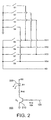
- FIG. 2 illustrates a front panel keyboard 200 that uses negative operational logic and can be used with the controller 110 shown in FIG. 1 .
- the front panel keyboard 200 includes a light 220, illustratively a light emitting diode (LED) D1, which is coupled to the light control line 150 through a transistor 210, which serves as a switch for the light 220.
- the collector of the transistor 210 is coupled to the light 220 though R15 and the base of the transistor 210 is coupled to a resistor R14 in the light control line 150.
- the resistance of R14 is selected such that when the microprocessor 115 applies a light control voltage to the light control line 150, the voltage at the base of the transistor 210 should be sufficiently high to turn on the transistor 210, so that the light 220 is turned on.
- the resistances of R14 and R15 are 10 kilo-ohms and 125 ohms, respectively.
- the front panel keyboard 200 illustratively includes eight keys, represented by switches S1-S8.
- the number of the keys can be different depending on the need of an application.
- the eight keys form four pairs: S1 and S5, S2 and S6, S3 and S7, and S4 and S8.
- Each pair shares one of the keyboard sense lines KS1-KS4.
- S1 and S5 share KS1, S2 and S6 share KS2, S3 and S7 share KS3, and S4 and S8 share KS4.
- One terminal of a key is coupled to a keyboard sense line, while the other terminal is coupled to ground. Since the type of operational logic is negative, no keyboard operational voltage is available in the front panel keyboard 200, and no identification voltage is applied.
- bit 7 of the keyboard control register 121 in the FPGA 120 of the controller 110 is set to a logic zero, and the microprocessor 115 determines that the type of operational logic of the front panel keyboard 200 is negative. Consequently, the microcontroller 115 sets bit 6 of the keyboard control register to a logic zero, which keeps the switch 130 in a condition with the P-MOS transistor 510 conducting and the N-MOS pull-down transistor 520 in a non-conductive state.
- the output of switch 130 provides roughly 3.3V to the keyboard control line 145, and provides a keyboard operational voltage for the keyboard 200 through the keyboard pull-up resistors R5-R8. In effect, the keyboard operational voltage is the source voltage for the keyboard pull-up resistors R5-R8.
- the microprocessor 115 periodically reads the keyboard control register 121.
- the receivers (input buffers) 131-135 receive a voltage of about the same magnitude of the keyboard operational voltage source, which is illustratively 3.3 volts, setting bits 1-4 to a logic one.
- the received voltage by the receiver is low.
- the received voltage is approximately equivalent to the voltage developed across the corresponding one of R9-R12, the resistance of which is only 100 ohms.
- the received voltage is close to zero volts, setting the corresponding one of bits 1-4 to a logic zero.
- KS1 is pulled low and bit 1 is set to logic zero.
- the microprocessor 115 detects that bit 1 has a logic value of zero, the microprocessor 115 starts to scan the keyboard 200.
- KD is set low to allow a key press on any of the 8 buttons to be detected.
- the scan process includes sensing the state of KS 1 by continuously reading bit 1, while setting the keyboard drive line KD high to determine which one of the two buttons (S1 or S5) is activated.
- the microprocessor 115 sets the keyboard drive line KD high by setting bit 5 to a logic one, resulting in applying a keyboard drive voltage to the keyboard drive line KD.
- the microprocessor 115 sets the keyboard drive line KD high and bit 1 retains a value of logic zero, i.e., the KS 1 remains low, the microprocessor 115 determines that key S1 is activated. Otherwise, if bit 1 is changed to a logic one, the microprocessor determines that key S5 is activated.
- the reason that the change of bit 1 from a logic zero to a logic one indicates that key S5 is activated is that the applied keyboard drive voltage in the keyboard drive line KD is coupled to the keyboard sense line KS1 through the closure of key S5, causing the keyboard sense line KS1 in a high state.
- the microprocessor 115 sets the keyboard drive line KD to low by setting bit 5 to zero, resulting in no voltage being applied to the keyboard drive line KD.
- the microprocessor 115 delays for a predetermined time, such as 5 milliseconds, before repeating the scanning process to verity that the key closure was not due to "key bounce." With the process described above, the microprocessor 115 can detect activation from any of the eight keys.
- FIG. 3 illustrates a front keyboard array 300 that uses positive operational logic and can be used with the controller 110 shown in FIG. 1 .
- the front panel keyboard 300 includes a light 320, illustratively a LED D', which is coupled to the light control line 150 through a transistor 310.
- the collector of the transistor 310 is coupled to the light 320 though R15' and the base of the transistor 310 is coupled to a resistor R14' to the light control line 150.
- the resistance of R14' is selected such that when the microprocessor 115 applies a light control voltage to the light control line 150, the voltage at the base of the transistor 310 should be sufficiently high to turn on the transistor 310, so that the light is turned on.
- the resistances of R14' and R15' are 10 kilo-ohms and 125 ohms, respectively.
- the front panel keyboard 300 includes eight keys represented by switches S'1-S'8.
- the eight keys form four pairs, each sharing a keyboard sense line.
- a keyboard operational voltage source for example, 5 volts
- one terminal of each key is coupled to the operational voltage source.
- a difference between the front panel keyboard 300 and the front panel keyboard 200 is that the front panel keyboard 300 applies an identification voltage to the light control line 150 by coupling the keyboard operational voltage source (for example, 5 volts) to the light control line 150 at a junction 330 through a resistor R6, illustratively 18 kilo-ohms.
- the magnitudes of the keyboard operational voltage source, R6, and R14 are selected such that the voltage received by the receiver 136 is above the first threshold, so that bit 7 of the keyboard control register is set to a logic one, indicating that the type of operational logic of the front panel keyboard 300 is positive.
- the voltage received by the receiver 136 is about 2.2 volts, which represents a logic one.
- the microprocessor 115 determines that the type of operational logic of the front panel keyboard 300 is positive and sets bit 6 to a logic one, decoupling the keyboard operational voltage source in the FPGA 120 from the keyboard control line 145.
- the signal in the keyboard drive line KD is inverted by an inverter u1 an an AND gate (one of u3-u6) is added at the output terminal of each of keys S'5-S'8.
- the AND gate produces an output coupled to the corresponding keyboard sense line from the output of one of the keys S'5-S'8 and the inverted signal in the keyboard drive line KD.
- resistors R301, R302, R303 and R304 provide a logic zero level into U3-U6 when no keyboard buttons are pressed.
- the line state of a keyboard sense line during rest and active states in the front panel keyboard 300 is the inverse of that of the front panel keyboard 200.
- the receivers receive a voltage of zero volt, i.e., the corresponding keyboard sense line is low, setting bits 1-4 to a logic zero.
- the received voltage by the corresponding receiver is about the same magnitude of the operational voltage source, which is illustratively 5 volts, setting a corresponding one of bits 1-4 of the keyboard control register 121 in the FPGA 120 to a logic one.
- the operational voltage source is coupled to the keyboard sense line KS 1, setting bit 1 to a logic one.
- Activating the key S'5 also couples the operation voltage source to the keyboard sense line KS 1.
- the microprocessor 115 normally does not apply a voltage to the keyboard drive line KD, the inverted signal is a logic one.
- the AND gate u3 produces a logic one at the keyboard sense line KS 1, which is about 2-5 volts, again setting bit 1 to a logic one.
- the microprocessor 115 detects that bit 1 has a logic value of one, the microprocessor 115 starts to scan the keyboard 300.
- the microprocessor 115 sets the keyboard drive line KD high and bit 1 retains a value of a logic one, i.e., the KS1 remains high, the microprocessor 115 determines that key S' 1 is activated. Otherwise, if bit 1 is changed to a logic zero, the microprocessor determines that key S'5 is activated. The reason that the change of state of bit 1 indicates that key S'5 is activated is that even though the input from the activation of the key S'5 is high (a logic one), the inverted signal in KD is a logic zero, causing the output of the AND gate u3 to a logic zero. The microprocessor 115 then sets the keyboard drive line KD to low. With the process described above, the microprocessor 115 again can detect activation from any of the eight keys.
- the LEDs D1 and D1' are LEDs having a forward voltage of about 2.5 volts at 20 milliamperes (mA). LEDs with different forward voltages can be used as well but the resistance of the series resistor (R15 or RC should be recalculated.
- the transistors 210 and 310 are illustratively generic BC847B surface-mounted transistors with a Beta (current gain) of about 100 at 20 mA and a forward voltage (V be-on ) from the base to the emitter of 0.7 volts. Any transistor with a similar Beta at 20 mA and a V be-on of approximately 0.7 volts can be used as well.
- R15 and R15' are calculated based on a 5-volt source for the respective LED D1 and D1' having the illustrated properties discussed above. If the current ratings of LED D1 and D1' are changed, the resistances of R15 and R15' should be changed as well. For example, if the current is increased from 20 mA to 25 mA, the resistances of R15 and R15'should be decreased from 125 ohms to 100 ohms.
- the resistances of R14 and R14' are determined based on the illustrative properties of the LED D1 and D1'. If the Beta of the LEDs increases, the resistances of R14 and R14' can be increased as well.
- the combination of V be-on and the current through R14' from R6 determine the identification voltage present at the light control line 150.
- the identification voltage present at the light control line 150 is about 2.2 volts.
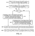
- FIG. 4 is an illustrative method of detecting a type of operational logic of a front panel keyboard of a television apparatus, detecting a key activation signal from the front panel keyboard, and scanning the front panel keyboard to determine which key has been activated, according to the principles of the invention.
- the television apparatus includes a controller for receiving a key activation signal from the front panel keyboard.
- the controller applies a light control voltage to turn on a light in the front panel keyboard through a light control line.
- the function of step 410 is to light up the front panel keyboard for a user to see each key in the keyboard more clearly. As such, step 410 is optional.
- the controller detects an identification voltage applied by the front panel keyboard to a first control line.
- the first and light control lines can be different control lines or the same control line, and the light control and identification voltages should be voltages representing logic one.
- the controller determines that the type of operational logic of the front panel keyboard is positive, and does not apply a keyboard operational voltage to the front panel keyboard through a keyboard control line, at step 440. Otherwise, if the detected second voltage is less than the second threshold, i.e., the identification voltage is not detected, the controller determines that the type of operational logic of the front panel keyboard is negative, and applies the keyboard operational voltage to the front panel keyboard through a keyboard control line at step 430. The controller then detects a key activation signal from the front panel keyboard at step 450, and scans the front panel keyboard to determine which key has been activated at step 460.
Landscapes
- Engineering & Computer Science (AREA)
- Multimedia (AREA)
- Signal Processing (AREA)
- Input From Keyboards Or The Like (AREA)
Applications Claiming Priority (3)
| Application Number | Priority Date | Filing Date | Title |
|---|---|---|---|
| US44860303P | 2003-02-14 | 2003-02-14 | |
| US448603P | 2003-02-14 | ||
| PCT/US2004/004209 WO2004075529A2 (en) | 2003-02-14 | 2004-02-12 | Apparatus in a tv receiver automatically detecting the type of keyboard attached thereto |
Publications (2)
| Publication Number | Publication Date |
|---|---|
| EP1597908A2 EP1597908A2 (en) | 2005-11-23 |
| EP1597908B1 true EP1597908B1 (en) | 2012-01-04 |
Family
ID=32908613
Family Applications (1)
| Application Number | Title | Priority Date | Filing Date |
|---|---|---|---|
| EP04710672A Expired - Lifetime EP1597908B1 (en) | 2003-02-14 | 2004-02-12 | Apparatus in a tv receiver automatically detecting the type of keyboard attached thereto |
Country Status (7)
| Country | Link |
|---|---|
| US (1) | US7679680B2 (ko) |
| EP (1) | EP1597908B1 (ko) |
| JP (1) | JP4532467B2 (ko) |
| KR (1) | KR101082133B1 (ko) |
| CN (1) | CN1751504B (ko) |
| MX (1) | MXPA05008594A (ko) |
| WO (1) | WO2004075529A2 (ko) |
Cited By (1)
| Publication number | Priority date | Publication date | Assignee | Title |
|---|---|---|---|---|
| CN106331875A (zh) * | 2016-09-05 | 2017-01-11 | 深圳Tcl数字技术有限公司 | 多面板按键控制方法及装置 |
Families Citing this family (5)
| Publication number | Priority date | Publication date | Assignee | Title |
|---|---|---|---|---|
| US20060115275A1 (en) * | 2004-12-01 | 2006-06-01 | Jiaxi Kan | Multiple rate optical transponder |
| TW200906071A (en) * | 2007-07-24 | 2009-02-01 | Beyond Innovation Tech Co Ltd | Key system and method capable of detecting if a plurality of keys are triggered |
| CN102543030A (zh) * | 2010-12-22 | 2012-07-04 | 鸿富锦精密工业(深圳)有限公司 | 数字视频界面驱动模组 |
| CN103279221A (zh) * | 2013-05-21 | 2013-09-04 | 北京小米科技有限责任公司 | 徽标组件、控制方法、控制器和电子设备 |
| JP2016086239A (ja) * | 2014-10-23 | 2016-05-19 | ファナック株式会社 | キーボード |
Family Cites Families (28)
| Publication number | Priority date | Publication date | Assignee | Title |
|---|---|---|---|---|
| JPS53131716A (en) | 1977-04-22 | 1978-11-16 | Mitsubishi Electric Corp | Digital signal transmission system |
| DE2756327C2 (de) * | 1977-12-17 | 1979-11-15 | Deutsche Itt Industries Gmbh, 7800 Freiburg | Schaltung sanordnung für eine Eingabetastatur |
| JPS5548273U (ko) * | 1978-09-27 | 1980-03-29 | ||
| DE3032337C3 (de) * | 1979-08-28 | 1994-08-11 | Canon Kk | Elektronische Einrichtung mit einer Wähleinrichtung zum Wählen eines beliebigen aus mehreren Empfangskanälen |
| US4279035A (en) * | 1979-12-27 | 1981-07-14 | Zenith Radio Corporation | Channel number entry system |
| US4318087A (en) * | 1980-09-08 | 1982-03-02 | Rca Corporation | Switch closure sensing circuit |
| DE3273873D1 (en) * | 1981-04-03 | 1986-11-20 | Commissariat Energie Atomique | Capacitive keyboard with anti-parasite structure |
| GB8305011D0 (en) * | 1983-02-23 | 1983-03-30 | Microwriter Ltd | Computer apparatus and remote keyboards |
| US4626830A (en) * | 1984-06-18 | 1986-12-02 | Motorola, Inc. | Membrane keyboard with identifying connectors |
| JPS63182730A (ja) | 1987-01-26 | 1988-07-28 | Hitachi Ltd | 入力装置制御方式 |
| US6014092A (en) * | 1987-10-14 | 2000-01-11 | Universal Electronics Inc. | Key mover |
| JPH0348180A (ja) * | 1989-04-27 | 1991-03-01 | Casio Comput Co Ltd | スイッチ状態高速検出装置 |
| US5036261A (en) * | 1989-08-11 | 1991-07-30 | Thomson Consumer Electronics, Inc. | Standby/run power supply and control circuit |
| JPH03176714A (ja) | 1989-12-06 | 1991-07-31 | Hitachi Ltd | 情報処理装置 |
| JPH04211820A (ja) | 1991-02-12 | 1992-08-03 | Sanyo Electric Co Ltd | キーボード識別方式 |
| JP3105015B2 (ja) * | 1991-03-25 | 2000-10-30 | パイオニア株式会社 | Catvシステムにおける端末装置 |
| WO1994028634A1 (en) * | 1993-05-21 | 1994-12-08 | Arthur D. Little Enterprises, Inc. | User-configurable control device |
| JPH082126A (ja) * | 1994-06-17 | 1996-01-09 | Sony Corp | 昇華熱転写インクリボン |
| JPH0973352A (ja) | 1995-09-06 | 1997-03-18 | Nec Corp | キーボードインタフェース回路 |
| CA2188707C (en) * | 1995-11-13 | 2000-08-01 | Aaron Hal Dinwiddie | System providing freeze of closed captioning data |
| CN1058825C (zh) * | 1997-02-20 | 2000-11-22 | 明碁电脑股份有限公司 | 显示器画面功能调整方法及装置 |
| US5872561A (en) * | 1997-03-31 | 1999-02-16 | Allen-Bradley Company, Llc | Fast scanning switch matrix |
| KR100276257B1 (ko) * | 1997-04-07 | 2000-12-15 | 이형도 | 전원공급장치 판별기능을 갖는 유무선 겸용키보드장치 및 그 제어방법 |
| WO1999024962A1 (en) * | 1997-11-12 | 1999-05-20 | Think Outside | System and method for detecting key actuation in a keyboard |
| US6011328A (en) * | 1998-04-08 | 2000-01-04 | Terry L. Smith | Electric power lockout apparatus |
| TW501060B (en) * | 2000-07-12 | 2002-09-01 | Winbond Electronics Corp | Multiple selection architecture for the keyboard containing manufacturer identification code and matrix, and the selection method |
| KR100444630B1 (ko) * | 2002-01-28 | 2004-08-21 | 엘지전자 주식회사 | 키보드 제어기를 내장한 마이크로 컴퓨터 |
| WO2004098181A1 (en) * | 2003-04-25 | 2004-11-11 | Thomson Licensing S.A. | Variable intensity illumination device with detection and control circuit for a front panel of a television apparatus |
-
2004
- 2004-02-12 EP EP04710672A patent/EP1597908B1/en not_active Expired - Lifetime
- 2004-02-12 JP JP2006503541A patent/JP4532467B2/ja not_active Expired - Fee Related
- 2004-02-12 CN CN2004800041044A patent/CN1751504B/zh not_active Expired - Fee Related
- 2004-02-12 WO PCT/US2004/004209 patent/WO2004075529A2/en active Application Filing
- 2004-02-12 US US10/544,751 patent/US7679680B2/en active Active
- 2004-02-12 MX MXPA05008594A patent/MXPA05008594A/es not_active Application Discontinuation
- 2004-02-12 KR KR1020057014912A patent/KR101082133B1/ko not_active IP Right Cessation
Cited By (1)
| Publication number | Priority date | Publication date | Assignee | Title |
|---|---|---|---|---|
| CN106331875A (zh) * | 2016-09-05 | 2017-01-11 | 深圳Tcl数字技术有限公司 | 多面板按键控制方法及装置 |
Also Published As
| Publication number | Publication date |
|---|---|
| US20060087597A1 (en) | 2006-04-27 |
| MXPA05008594A (es) | 2006-03-13 |
| KR20050101337A (ko) | 2005-10-21 |
| JP4532467B2 (ja) | 2010-08-25 |
| JP2006518079A (ja) | 2006-08-03 |
| WO2004075529A2 (en) | 2004-09-02 |
| KR101082133B1 (ko) | 2011-11-09 |
| CN1751504A (zh) | 2006-03-22 |
| WO2004075529A3 (en) | 2005-02-10 |
| CN1751504B (zh) | 2010-05-26 |
| EP1597908A2 (en) | 2005-11-23 |
| US7679680B2 (en) | 2010-03-16 |
Similar Documents
| Publication | Publication Date | Title |
|---|---|---|
| JP3698439B2 (ja) | データ通信バスを有する回路 | |
| KR0148018B1 (ko) | 텔레비젼 신호 스위칭 시스템 | |
| US5469082A (en) | Peripheral component interfacing system with bus voltage/logic supply comparison means | |
| US6259171B1 (en) | Hot-swap device preventing system crash when switching power source | |
| US5672917A (en) | Semiconductor power switch system | |
| KR100288581B1 (ko) | 리모콘을 이용한 복수개 모니터의 파워 온/오프 방법 | |
| EP1597908B1 (en) | Apparatus in a tv receiver automatically detecting the type of keyboard attached thereto | |
| US5495301A (en) | Three wire pillow speaker with full television remote control functions | |
| US5557236A (en) | Integrated circuit with bidirectional pin | |
| US5886426A (en) | Power switch locking device | |
| WO2009156831A2 (en) | Standby circuit and electric appliance comprising such a circuit | |
| US5945865A (en) | Full-swing high voltage data latch | |
| KR930005929Y1 (ko) | 자동모드 절환회로 | |
| JPH07154234A (ja) | 信号入出力切替装置 | |
| JP3490044B2 (ja) | パワー半導体回路 | |
| KR101083397B1 (ko) | 신호 처리 시스템 | |
| KR0121487Y1 (ko) | 밧데리상태 디스플레이장치 | |
| KR100297435B1 (ko) | 리모콘의슬라이드식스위칭회로 | |
| JP2000047764A (ja) | 電源システム | |
| KR0159721B1 (ko) | 프린터의 전원 제어회로 | |
| KR100461635B1 (ko) | 리셋회로 | |
| KR0132212Y1 (ko) | 엘리베이터 스위치 제어회로 | |
| KR0119486Y1 (ko) | 리모콘 신호 수신 확인회로 | |
| KR970004895B1 (ko) | 헤드폰 스테레오용 리모트 제어회로 | |
| KR950013164B1 (ko) | 멀티기기의 다용도 리모콘 장치 및 그 제어방법 |
Legal Events
| Date | Code | Title | Description |
|---|---|---|---|
| PUAI | Public reference made under article 153(3) epc to a published international application that has entered the european phase |
Free format text: ORIGINAL CODE: 0009012 |
|
| 17P | Request for examination filed |
Effective date: 20050905 |
|
| AK | Designated contracting states |
Kind code of ref document: A2 Designated state(s): AT BE BG CH CY CZ DE DK EE ES FI FR GB GR HU IE IT LI LU MC NL PT RO SE SI SK TR |
|
| AX | Request for extension of the european patent |
Extension state: AL LT LV MK |
|
| DAX | Request for extension of the european patent (deleted) | ||
| RBV | Designated contracting states (corrected) |
Designated state(s): DE ES FR GB IT TR |
|
| RAP1 | Party data changed (applicant data changed or rights of an application transferred) |
Owner name: THOMSON LICENSING |
|
| GRAP | Despatch of communication of intention to grant a patent |
Free format text: ORIGINAL CODE: EPIDOSNIGR1 |
|
| GRAS | Grant fee paid |
Free format text: ORIGINAL CODE: EPIDOSNIGR3 |
|
| GRAA | (expected) grant |
Free format text: ORIGINAL CODE: 0009210 |
|
| AK | Designated contracting states |
Kind code of ref document: B1 Designated state(s): DE ES FR GB IT TR |
|
| REG | Reference to a national code |
Ref country code: GB Ref legal event code: FG4D |
|
| REG | Reference to a national code |
Ref country code: DE Ref legal event code: R096 Ref document number: 602004035961 Country of ref document: DE Effective date: 20120301 |
|
| REG | Reference to a national code |
Ref country code: DE Ref legal event code: R084 Ref document number: 602004035961 Country of ref document: DE Effective date: 20120316 |
|
| PGFP | Annual fee paid to national office [announced via postgrant information from national office to epo] |
Ref country code: GB Payment date: 20120223 Year of fee payment: 9 |
|
| PLBE | No opposition filed within time limit |
Free format text: ORIGINAL CODE: 0009261 |
|
| STAA | Information on the status of an ep patent application or granted ep patent |
Free format text: STATUS: NO OPPOSITION FILED WITHIN TIME LIMIT |
|
| PG25 | Lapsed in a contracting state [announced via postgrant information from national office to epo] |
Ref country code: IT Free format text: LAPSE BECAUSE OF FAILURE TO SUBMIT A TRANSLATION OF THE DESCRIPTION OR TO PAY THE FEE WITHIN THE PRESCRIBED TIME-LIMIT Effective date: 20120104 |
|
| 26N | No opposition filed |
Effective date: 20121005 |
|
| REG | Reference to a national code |
Ref country code: DE Ref legal event code: R097 Ref document number: 602004035961 Country of ref document: DE Effective date: 20121005 |
|
| PG25 | Lapsed in a contracting state [announced via postgrant information from national office to epo] |
Ref country code: ES Free format text: LAPSE BECAUSE OF FAILURE TO SUBMIT A TRANSLATION OF THE DESCRIPTION OR TO PAY THE FEE WITHIN THE PRESCRIBED TIME-LIMIT Effective date: 20120415 |
|
| GBPC | Gb: european patent ceased through non-payment of renewal fee |
Effective date: 20130212 |
|
| PG25 | Lapsed in a contracting state [announced via postgrant information from national office to epo] |
Ref country code: GB Free format text: LAPSE BECAUSE OF NON-PAYMENT OF DUE FEES Effective date: 20130212 |
|
| PG25 | Lapsed in a contracting state [announced via postgrant information from national office to epo] |
Ref country code: TR Free format text: LAPSE BECAUSE OF FAILURE TO SUBMIT A TRANSLATION OF THE DESCRIPTION OR TO PAY THE FEE WITHIN THE PRESCRIBED TIME-LIMIT Effective date: 20120104 |
|
| REG | Reference to a national code |
Ref country code: FR Ref legal event code: PLFP Year of fee payment: 13 |
|
| REG | Reference to a national code |
Ref country code: FR Ref legal event code: PLFP Year of fee payment: 14 |
|
| REG | Reference to a national code |
Ref country code: DE Ref legal event code: R082 Ref document number: 602004035961 Country of ref document: DE Representative=s name: DEHNS, DE Ref country code: DE Ref legal event code: R082 Ref document number: 602004035961 Country of ref document: DE Representative=s name: DEHNS PATENT AND TRADEMARK ATTORNEYS, DE Ref country code: DE Ref legal event code: R082 Ref document number: 602004035961 Country of ref document: DE Representative=s name: HOFSTETTER, SCHURACK & PARTNER PATENT- UND REC, DE |
|
| REG | Reference to a national code |
Ref country code: FR Ref legal event code: PLFP Year of fee payment: 15 |
|
| REG | Reference to a national code |
Ref country code: FR Ref legal event code: TP Owner name: THOMSON LICENSING DTV, FR Effective date: 20180830 |
|
| REG | Reference to a national code |
Ref country code: DE Ref legal event code: R082 Ref document number: 602004035961 Country of ref document: DE Representative=s name: DEHNS, DE Ref country code: DE Ref legal event code: R081 Ref document number: 602004035961 Country of ref document: DE Owner name: INTERDIGITAL MADISON PATENT HOLDINGS, FR Free format text: FORMER OWNER: THOMSON LICENSING, ISSY-LES-MOULINEAUX, FR Ref country code: DE Ref legal event code: R082 Ref document number: 602004035961 Country of ref document: DE Representative=s name: DEHNS PATENT AND TRADEMARK ATTORNEYS, DE |
|
| PGFP | Annual fee paid to national office [announced via postgrant information from national office to epo] |
Ref country code: FR Payment date: 20230223 Year of fee payment: 20 |
|
| PGFP | Annual fee paid to national office [announced via postgrant information from national office to epo] |
Ref country code: DE Payment date: 20230227 Year of fee payment: 20 |
|
| P01 | Opt-out of the competence of the unified patent court (upc) registered |
Effective date: 20230514 |
|
| REG | Reference to a national code |
Ref country code: DE Ref legal event code: R071 Ref document number: 602004035961 Country of ref document: DE |