EP1583142A2 - Procédé de déposition d'une couche isolante et dispositif semiconducteur - Google Patents
Procédé de déposition d'une couche isolante et dispositif semiconducteur Download PDFInfo
- Publication number
- EP1583142A2 EP1583142A2 EP05007007A EP05007007A EP1583142A2 EP 1583142 A2 EP1583142 A2 EP 1583142A2 EP 05007007 A EP05007007 A EP 05007007A EP 05007007 A EP05007007 A EP 05007007A EP 1583142 A2 EP1583142 A2 EP 1583142A2
- Authority
- EP
- European Patent Office
- Prior art keywords
- insulating film
- deposition
- film
- gas
- dielectric constant
- Prior art date
- Legal status (The legal status is an assumption and is not a legal conclusion. Google has not performed a legal analysis and makes no representation as to the accuracy of the status listed.)
- Withdrawn
Links
Images


Classifications
-
- C—CHEMISTRY; METALLURGY
- C09—DYES; PAINTS; POLISHES; NATURAL RESINS; ADHESIVES; COMPOSITIONS NOT OTHERWISE PROVIDED FOR; APPLICATIONS OF MATERIALS NOT OTHERWISE PROVIDED FOR
- C09D—COATING COMPOSITIONS, e.g. PAINTS, VARNISHES OR LACQUERS; FILLING PASTES; CHEMICAL PAINT OR INK REMOVERS; INKS; CORRECTING FLUIDS; WOODSTAINS; PASTES OR SOLIDS FOR COLOURING OR PRINTING; USE OF MATERIALS THEREFOR
- C09D4/00—Coating compositions, e.g. paints, varnishes or lacquers, based on organic non-macromolecular compounds having at least one polymerisable carbon-to-carbon unsaturated bond ; Coating compositions, based on monomers of macromolecular compounds of groups C09D183/00 - C09D183/16
-
- C—CHEMISTRY; METALLURGY
- C23—COATING METALLIC MATERIAL; COATING MATERIAL WITH METALLIC MATERIAL; CHEMICAL SURFACE TREATMENT; DIFFUSION TREATMENT OF METALLIC MATERIAL; COATING BY VACUUM EVAPORATION, BY SPUTTERING, BY ION IMPLANTATION OR BY CHEMICAL VAPOUR DEPOSITION, IN GENERAL; INHIBITING CORROSION OF METALLIC MATERIAL OR INCRUSTATION IN GENERAL
- C23C—COATING METALLIC MATERIAL; COATING MATERIAL WITH METALLIC MATERIAL; SURFACE TREATMENT OF METALLIC MATERIAL BY DIFFUSION INTO THE SURFACE, BY CHEMICAL CONVERSION OR SUBSTITUTION; COATING BY VACUUM EVAPORATION, BY SPUTTERING, BY ION IMPLANTATION OR BY CHEMICAL VAPOUR DEPOSITION, IN GENERAL
- C23C16/00—Chemical coating by decomposition of gaseous compounds, without leaving reaction products of surface material in the coating, i.e. chemical vapour deposition [CVD] processes
- C23C16/22—Chemical coating by decomposition of gaseous compounds, without leaving reaction products of surface material in the coating, i.e. chemical vapour deposition [CVD] processes characterised by the deposition of inorganic material, other than metallic material
- C23C16/30—Deposition of compounds, mixtures or solid solutions, e.g. borides, carbides, nitrides
- C23C16/40—Oxides
- C23C16/401—Oxides containing silicon
-
- C—CHEMISTRY; METALLURGY
- C23—COATING METALLIC MATERIAL; COATING MATERIAL WITH METALLIC MATERIAL; CHEMICAL SURFACE TREATMENT; DIFFUSION TREATMENT OF METALLIC MATERIAL; COATING BY VACUUM EVAPORATION, BY SPUTTERING, BY ION IMPLANTATION OR BY CHEMICAL VAPOUR DEPOSITION, IN GENERAL; INHIBITING CORROSION OF METALLIC MATERIAL OR INCRUSTATION IN GENERAL
- C23C—COATING METALLIC MATERIAL; COATING MATERIAL WITH METALLIC MATERIAL; SURFACE TREATMENT OF METALLIC MATERIAL BY DIFFUSION INTO THE SURFACE, BY CHEMICAL CONVERSION OR SUBSTITUTION; COATING BY VACUUM EVAPORATION, BY SPUTTERING, BY ION IMPLANTATION OR BY CHEMICAL VAPOUR DEPOSITION, IN GENERAL
- C23C16/00—Chemical coating by decomposition of gaseous compounds, without leaving reaction products of surface material in the coating, i.e. chemical vapour deposition [CVD] processes
- C23C16/44—Chemical coating by decomposition of gaseous compounds, without leaving reaction products of surface material in the coating, i.e. chemical vapour deposition [CVD] processes characterised by the method of coating
- C23C16/50—Chemical coating by decomposition of gaseous compounds, without leaving reaction products of surface material in the coating, i.e. chemical vapour deposition [CVD] processes characterised by the method of coating using electric discharges
- C23C16/505—Chemical coating by decomposition of gaseous compounds, without leaving reaction products of surface material in the coating, i.e. chemical vapour deposition [CVD] processes characterised by the method of coating using electric discharges using radio frequency discharges
- C23C16/509—Chemical coating by decomposition of gaseous compounds, without leaving reaction products of surface material in the coating, i.e. chemical vapour deposition [CVD] processes characterised by the method of coating using electric discharges using radio frequency discharges using internal electrodes
-
- H—ELECTRICITY
- H10—SEMICONDUCTOR DEVICES; ELECTRIC SOLID-STATE DEVICES NOT OTHERWISE PROVIDED FOR
- H10P—GENERIC PROCESSES OR APPARATUS FOR THE MANUFACTURE OR TREATMENT OF DEVICES COVERED BY CLASS H10
- H10P14/00—Formation of materials, e.g. in the shape of layers or pillars
- H10P14/60—Formation of materials, e.g. in the shape of layers or pillars of insulating materials
- H10P14/65—Formation of materials, e.g. in the shape of layers or pillars of insulating materials characterised by treatments performed before or after the formation of the materials
- H10P14/6516—Formation of materials, e.g. in the shape of layers or pillars of insulating materials characterised by treatments performed before or after the formation of the materials of treatments performed after formation of the materials
- H10P14/6548—Formation of materials, e.g. in the shape of layers or pillars of insulating materials characterised by treatments performed before or after the formation of the materials of treatments performed after formation of the materials by forming intermediate materials, e.g. capping layers or diffusion barriers
-
- H—ELECTRICITY
- H10—SEMICONDUCTOR DEVICES; ELECTRIC SOLID-STATE DEVICES NOT OTHERWISE PROVIDED FOR
- H10W—GENERIC PACKAGES, INTERCONNECTIONS, CONNECTORS OR OTHER CONSTRUCTIONAL DETAILS OF DEVICES COVERED BY CLASS H10
- H10W20/00—Interconnections in chips, wafers or substrates
- H10W20/01—Manufacture or treatment
- H10W20/031—Manufacture or treatment of conductive parts of the interconnections
- H10W20/032—Manufacture or treatment of conductive parts of the interconnections of conductive barrier, adhesion or liner layers
- H10W20/038—Manufacture or treatment of conductive parts of the interconnections of conductive barrier, adhesion or liner layers covering conductive structures
-
- H—ELECTRICITY
- H10—SEMICONDUCTOR DEVICES; ELECTRIC SOLID-STATE DEVICES NOT OTHERWISE PROVIDED FOR
- H10W—GENERIC PACKAGES, INTERCONNECTIONS, CONNECTORS OR OTHER CONSTRUCTIONAL DETAILS OF DEVICES COVERED BY CLASS H10
- H10W20/00—Interconnections in chips, wafers or substrates
- H10W20/01—Manufacture or treatment
- H10W20/071—Manufacture or treatment of dielectric parts thereof
- H10W20/081—Manufacture or treatment of dielectric parts thereof by forming openings in the dielectric parts
- H10W20/084—Manufacture or treatment of dielectric parts thereof by forming openings in the dielectric parts for dual-damascene structures
-
- H—ELECTRICITY
- H10—SEMICONDUCTOR DEVICES; ELECTRIC SOLID-STATE DEVICES NOT OTHERWISE PROVIDED FOR
- H10P—GENERIC PROCESSES OR APPARATUS FOR THE MANUFACTURE OR TREATMENT OF DEVICES COVERED BY CLASS H10
- H10P14/00—Formation of materials, e.g. in the shape of layers or pillars
- H10P14/60—Formation of materials, e.g. in the shape of layers or pillars of insulating materials
- H10P14/63—Formation of materials, e.g. in the shape of layers or pillars of insulating materials characterised by the formation processes
- H10P14/6326—Deposition processes
- H10P14/6328—Deposition from the gas or vapour phase
- H10P14/6334—Deposition from the gas or vapour phase using decomposition or reaction of gaseous or vapour phase compounds, i.e. chemical vapour deposition
- H10P14/6336—Deposition from the gas or vapour phase using decomposition or reaction of gaseous or vapour phase compounds, i.e. chemical vapour deposition in the presence of a plasma [PECVD]
-
- H—ELECTRICITY
- H10—SEMICONDUCTOR DEVICES; ELECTRIC SOLID-STATE DEVICES NOT OTHERWISE PROVIDED FOR
- H10P—GENERIC PROCESSES OR APPARATUS FOR THE MANUFACTURE OR TREATMENT OF DEVICES COVERED BY CLASS H10
- H10P14/00—Formation of materials, e.g. in the shape of layers or pillars
- H10P14/60—Formation of materials, e.g. in the shape of layers or pillars of insulating materials
- H10P14/66—Formation of materials, e.g. in the shape of layers or pillars of insulating materials characterised by the type of materials
- H10P14/668—Formation of materials, e.g. in the shape of layers or pillars of insulating materials characterised by the type of materials the materials being characterised by the deposition precursor materials
- H10P14/6681—Formation of materials, e.g. in the shape of layers or pillars of insulating materials characterised by the type of materials the materials being characterised by the deposition precursor materials the precursor containing a compound comprising Si
- H10P14/6684—Formation of materials, e.g. in the shape of layers or pillars of insulating materials characterised by the type of materials the materials being characterised by the deposition precursor materials the precursor containing a compound comprising Si the compound comprising silicon and oxygen
- H10P14/6686—Formation of materials, e.g. in the shape of layers or pillars of insulating materials characterised by the type of materials the materials being characterised by the deposition precursor materials the precursor containing a compound comprising Si the compound comprising silicon and oxygen the compound being a molecule comprising at least one silicon-oxygen bond and the compound having hydrogen or an organic group attached to the silicon or oxygen, e.g. a siloxane
-
- H—ELECTRICITY
- H10—SEMICONDUCTOR DEVICES; ELECTRIC SOLID-STATE DEVICES NOT OTHERWISE PROVIDED FOR
- H10P—GENERIC PROCESSES OR APPARATUS FOR THE MANUFACTURE OR TREATMENT OF DEVICES COVERED BY CLASS H10
- H10P14/00—Formation of materials, e.g. in the shape of layers or pillars
- H10P14/60—Formation of materials, e.g. in the shape of layers or pillars of insulating materials
- H10P14/69—Inorganic materials
- H10P14/692—Inorganic materials composed of oxides, glassy oxides or oxide-based glasses
- H10P14/6921—Inorganic materials composed of oxides, glassy oxides or oxide-based glasses containing silicon
- H10P14/6922—Inorganic materials composed of oxides, glassy oxides or oxide-based glasses containing silicon the material containing Si, O and at least one of H, N, C, F or other non-metal elements, e.g. SiOC, SiOC:H or SiONC
Definitions
- the present invention relates to a deposition method and a semiconductor device, particularly to a deposition method for forming an insulating film that covers wirings mainly made of copper film and has low dielectric constant and a semiconductor device having the insulating film formed thereon.
- a multilayer wiring structure with small RC delay time has been demanded.
- wirings mainly made of copper having a small electric resistance are used as wirings, and an insulating film having a low dielectric constant (hereinafter, referred to as a low dielectric constant insulating film) is used as a barrier insulating film covering the wirings mainly made of copper and/or a primary insulating film on the barrier insulating film.
- a deposition method by a coating method and a deposition method by a plasma-enhanced CVD method are known as a deposition method for forming the low dielectric constant insulating film.
- an insulating film deposited by the plasma-enhanced CVD method has a larger relative dielectric constant comparing to the insulating film deposited by the coating method, it has higher mechanical strength and smaller moisture content, so that research and development of a deposition method of the low dielectric constant insulating film by the plasma-enhanced CVD method has been diligently done.
- Patent Documents 1, 2, 3 and the like describe the deposition method of the low dielectric constant insulating film such as the barrier insulating film and the primary insulating film on the barrier insulating film by the plasma-enhanced CVD method.
- the inventors found out that when chain siloxane or organic silane having at least one of methyl group and methoxy group was added to the cyclic siloxane having at least one of methyl group and methoxy group, the white turbidity did not occur although the relative dielectric constant was increased corresponding to an added amount thereof. Consequently, it was made clear that the mechanical strength could be improved, the moisture absorbing characteristics could be improved and the relative dielectric constant could be maintained low by adjusting the flow rate of chain siloxane or organic siloxane to cyclic siloxane. Further, it was made clear that the film also had the copper diffusion preventing function. Particularly, it was made clear that the use of siloxane or organic silane containing methoxy group was effective in increasing the mechanical strength.
- deposition is performed by a plasma-enhanced CVD method using a deposition gas having a gas mixture of the cyclic siloxane having at least one of methyl group and methoxy group and the chain siloxane having at least one of methyl group and methoxy group as a primary constituent gas.
- deposition is performed by a plasma-enhanced CVD method using a deposition gas having a gas mixture of the cyclic siloxane having at least one of methyl group and methoxy group and the organic silane having at least one of methyl group and methoxy group as a primary constituent gas.
- deposition is performed by a plasma-enhanced CVD method using a deposition gas where oxidizing gas such as H 2 O is further added to the gas mixture.
- inert gas as diluting gas
- rapid reaction of deposition gas can be suppressed and vapor phase reaction can be suppressed. This prevents the reduction of the mechanical strength and adhesion strength of the formed film, and also prevents the generation of particles.
- this deposition method is applied for a semiconductor device in which copper wirings and the like are formed.
- the insulating film having the above-described characteristic is used as a barrier insulating film covering the copper wirings and the like, as an insulating film directly covering the copper wirings and the like, or as a primary insulating film on the barrier insulating film covering the copper wirings and the like.
- the above-described insulating film or the barrier insulating film and the primary insulating film are used as an insulating film that constitutes a wiring interlayer insulating film or a wiring buried insulating film.
- Fig. 1 is the side view showing the constitution of a parallel plate type plasma deposition apparatus 101 used in the deposition method according to the embodiments of the present invention.
- the parallel plate type plasma-enhanced CVD deposition apparatus 101 is made up of a deposition section 101A, which is a place of forming the insulating film on a substrate 21 subject to deposition by plasma gas, and a deposition gas supply section 101B having supply sources of a plurality of gases that constitute the deposition gas.
- the deposition section 101A as shown in Fig. 1, comprises a chamber 1 in which pressure can be reduced, where the chamber 1 is connected to an exhaust unit 6 via an exhaust pipe 4.
- An opening/closing valve 5 that controls communication/non-communication between the chamber 1 and the exhaust unit 6 is provided halfway the exhaust pipe 4.
- the chamber 1 is provided with pressure measurement means such as a vacuum meter (not shown) for monitoring the pressure inside the chamber 1.
- the chamber 1 is provided with a pair of an upper electrode (first electrode) 2 and a lower electrode (second electrode) 3 which oppose to each other.
- a high-frequency power supply source (RF power source) 7 which supplies high-frequency power having the frequency of 13.56 MHz, is connected to the upper electrode 2, and a low-frequency power supply source 8, which supplies low-frequency power having the frequency of 380 kHz, is connected to the lower electrode 3.
- the power supply sources 7, 8 supply power to the upper electrode 2 and the lower electrode 3, and thus the deposition gas is transformed into plasma.
- the upper electrode 2, the lower electrode 3, and the power sources 7, 8 constitute plasma generation means that transforms the deposition gas into plasma.
- the upper electrode 2 serves as a distributor of the deposition gas.
- a plurality of through holes are formed in the upper electrode 2, and openings of the through holes at the opposing surface to the lower electrode 3 are discharge ports (introduction ports) of the deposition gas.
- the discharge ports of the deposition gas or the like is connected to the deposition gas supply section 101B via piping 9a.
- the upper electrode 2 is provided with a heater (not shown) depending on circumstances. The heater is used to heat the upper electrode 2 to the temperature of about 100°C to 200°C during deposition to prevent particles made of reactive products of the deposition gas or the like from adhering to the upper electrode 2.
- the lower electrode 3 serves as a holding stage for the substrate 21 subject to deposition, and is provided with a heater 12 heating the substrate 21 subject to deposition on the holding stage.
- the deposition gas supply section 101B is provided with a supply source of cyclic siloxane (first silicon containing organic compound) having at least one of methyl group and methoxy group, a supply source of chain siloxane (second silicon containing organic compound) having at least one of methyl group and methoxy group, a supply source of organic silane where at least one of methyl group and methoxy group has bonded silicon, a supply source of oxidizing gas made of any one of H 2 O, O 2 , N 2 O and CO 2 , a supply source of alcohol such as methyl alcohol (CH 3 OH) and ethyl alcohol (C 2 H 5 OH), a supply source of diluting gas, and a supply source of nitrogen (N 2 ).
- a supply source of cyclic siloxane first silicon containing organic compound
- second silicon containing organic compound having at least one of methyl group and methoxy group
- a supply source of organic silane where at least one of methyl group and methoxy group has bonded
- the gases are accordingly supplied into the chamber 1 through branch piping (9b to 9h) and piping 9a to which all the branch piping (9b to 9h) are connected.
- Flow rate adjusting means (11a to 11g) and opening/closing means (10b to 10o) for controlling communication/non-communication of the branch piping (9b to 9h) are installed halfway the branch piping (9b to 9h), and opening/closing means 10a for opening/closing the piping 9a is installed halfway the piping 9a.
- opening/closing means (10p to 10u) for controlling communication/non-communication between the branch piping 9h connected to the supply source of N 2 gas and the other branch piping (9b to 9g) are installed.
- N 2 gas purges not only the residual gas in the branch piping (9b to 9b) but also the residual gas in the piping 9a and the chamber 1.
- N 2 gas is used as diluting gas.
- the deposition apparatus 101 comprises the supply source of cyclic siloxane, the supply source of chain siloxane, the supply source of organic silane, the supply source of oxidizing gas, the supply source of alcohol, and the supply source of diluting gas, and also comprises plasma generation means (2, 3, 7, 8) that transform the deposition gas into plasma.
- the plasma generation means there exists means for generating plasma by the upper electrode 2 and the lower electrode 3 of the parallel plate type, for example, as the plasma generation means.
- the upper electrode 2 and the lower electrode 3 are subject to respective connections of the power supply sources (7, 8) that supply electric powers having two frequencies of high and low to the upper electrode 2 and the lower electrode 3, respectively. Therefore, the electric powers having two frequencies of high and low are respectively applied to respective electrodes (2,3) and thus plasma can be generated.
- the insulating film formed by applying low frequency electric power is much denser.
- At least the insulating film formed by applying high-frequency electric power has an even lower relative dielectric constant.
- the following gases can be used as representative examples regarding the deposition gas used in the present invention, which are the first silicon containing organic compound having cyclic siloxane bond and at least one of methyl group and methoxy group, the second silicon containing organic compound having straight-chain siloxane bond and at least one of methyl group and methoxy group, organic silane having at least one of methyl group and methoxy group, oxidizing gas, alcohol, and diluting gas.
- alcohol is vaporized in room temperature or by heating, and used in a gaseous state.
- the followings were made clear in the deposition method of the low dielectric constant insulating film by transforming into plasma the deposition gas which contains the primary constituent gas composing of the silicon containing organic compound, or of the silicon containing organic compound and the oxidizing gas.
- CH 3 , C 2 H 5 or the like is taken in the formed film to further reduce the relative dielectric constant by further adding methyl alcohol or ethyl alcohol to the above combination of gases, and bridge reaction in the formed film is enhanced by oxidation due to OH group, and thus the mechanical strength can be further increased.
- inert gas results in suppression of rapid reaction of deposition gas and thus in suppression of vapor phase reaction. If the vapor phase reaction occurs, the film quality of the formed film deteriorates drastically. For example, the mechanical strength or the adhesion strength of the formed film deteriorates. Moreover, it causes generation of particles, which is not preferable. Such problems can be prevented by suppressing the vapor phase reaction. Note that it is preferable to add an appropriate amount of inert gas because too much addition of inert gas results in a higher relative dielectric constant.
- a silicon oxide film was deposited on an Si substrate by a plasma enhanced CVD method (PECVD method) under the following deposition condition I.
- the deposition gas falls under the combination of 4-a described above. Specifically, OMCTS was used as the first silicon containing organic compound, HMDSO was used as the second silicon containing organic compound, H 2 O was used as the oxidizing gas, and He was used as the diluting gas.
- Figs. 3A to 3C show results of data acquisition when the deposition condition other than the HMDSO flow rate were fixed as shown in the deposition condition I and the HMDSO flow rate was changed within the range of 20 to 80 sccm.
- Figs. 4A to 4C show results of data acquisition when the deposition condition other than the H 2 O flow rate were fixed as shown in the deposition condition I and the H 2 O flow rate was changed within the range of 200 to 1000 sccm.
- Figs. 5A to 5C show results of data acquisition when the deposition condition other than the gas pressure were fixed as shown in the deposition condition I and the gas pressure was changed within the range of 1.0 to 2.0 Torr. Still further, Figs.
- 6A to 6C show results of data acquisition when the deposition condition other than the high-frequency power (frequency: 13.56 MHz) were fixed as shown in the deposition condition I and the high-frequency power (frequency: 13.56 MHz) was changed within the range of 350 to 650W.
- Fig. 3A is the view showing the relationship between the HMDSO flow rate of the deposition gas and the relative dielectric constant and the refraction index of the formed film.
- the left axis of ordinate denotes the relative dielectric constant of the formed film expressed in linear scale
- the right axis of ordinate denotes the refraction index of the formed film expressed in linear scale
- the axis of abscissas denotes the HMDSO flow rate (sccm) expressed in linear scale.
- the relative dielectric constant of the formed film gradually increases with the change of the HMDSO flow rate.
- the relative dielectric constant of about 2.25 when the HMDSO flow rate was 20 sccm became about 2.55 when the HMDSO flow rate was 30 sccm, it maintained an approximately constant value after that, and became about 2.55 when the HMDSO flow rate was 80 sccm.
- the low value of relative dielectric constant of 2.6 or less was obtained in the total survey range of the HMDSO flow rate from 20 to 80 sccm.
- the refraction index is shown as a guidepost for the density of the formed film. The higher the refraction index, the denser the film. The same applies to the followings and its explanation will be omitted.
- Fig. 3B is the view showing the relationship between the HMDSO flow rate of the deposition gas and the dielectric breakdown field of the formed film.
- the axis of ordinate shows the dielectric breakdown field (MV/cm) of the formed film expressed in linear scale
- the axis of abscissas shows the HMDSO flow rate (sccm) expressed in linear scale.
- the dielectric breakdown field gradually increases with the change of the HMDSO flow rate, and it became 5MV/cm or more in the total survey range of the HMDSO flow rate from 20 to 80 sccm. It was made clear that the film had sufficient dielectric breakdown voltage as the barrier insulating film.
- Fig. 3C is the view showing the relationship between the HMDSO flow rate of the deposition gas and the deposition rate of the formed film.
- the axis of ordinate shows the deposition rate (nm/min) of the formed film expressed in linear scale, and the axis of abscissas shows the HMDSO flow rate (sccm) expressed in linear scale.
- the deposition rate decreases in inverse proportion to the increase of the HMDSO flow rate.
- the deposition rate was about 700nm/min at the HMDSO flow rate of 20 sccm, and it was about 70nm/min at the flow rate of 80 sccm. It was found out that a practical level (presumably about 300nm/min) was at a small HMDSO flow rate.
- Fig. 4A is the view showing the relationship between the H 2 O flow rate of the deposition gas and the relative dielectric constant and the refraction index of the formed film.
- the left axis of ordinate denotes the relative dielectric constant of the formed film expressed in linear scale
- the right axis of ordinate denotes the refraction index of the formed film expressed in linear scale
- the axis of abscissas denotes the H 2 O flow rate (sccm) expressed in linear scale.
- the relative dielectric constant of the formed film gradually decreases with the change of the H 2 O flow rate.
- the relative dielectric constant of about 2.65 when the H 2 O flow rate was 200 sccm became about 2.55 when the H 2 O flow rate was 1000 sccm.
- the low value of relative dielectric constant of 2.6 or less was obtained in the range of the H 2 O flow rate from about 500 to 1000 sccm.
- Fig. 4B is the view showing the relationship between the H 2 O flow rate of deposition gas and the dielectric breakdown field of the formed film.
- the axis of ordinate shows the dielectric breakdown field (MV/cm) of the formed film expressed in linear scale
- the axis or abscissas shows the H 2 O flow rate (sccm) expressed in linear scale.
- An insulating film to be surveyed was formed on a copper film and the dielectric breakdown field was measured by using the copper film as one electrode. The same applies to the following measurement of dielectric breakdown field.
- the field gradually increased with the change of H 2 O flow rate, and it became 5MV/cm or more in the total survey range of the H 2 O flow rate from 200 to 1000 sccm. It was made clear that the film had sufficient dielectric breakdown voltage as the barrier insulating film. This shows that the insulating film has sufficient copper diffusion preventing function.
- Fig. 4C is the view showing the relationship between the H 2 O flow rate of deposition gas and the deposition rate of the formed film.
- the axis of ordinate shows the deposition rate (nm/min) of the formed film expressed in linear scale, and the axis or abscissas show the H 2 O flow rate (sccm) expressed in linear scale.
- the deposition rate showed substantially monotonic increase in proportion with the increase of the H 2 O flow rate.
- the deposition rate was about 30nm/min at the H 2 O flow rate of 200 sccm, and was about 500nm/min at the rate of 1000 sccm. It was found out that a practical level was at a large H 2 O flow rate.
- Fig.5A is the view showing the relationship between the gas pressure of the deposition gas and the relative dielectric constant and the refraction index of the formed film.
- the left axis of ordinate denotes the relative dielectric constant of the formed film expressed in linear scale
- the right axis of ordinate denotes the refraction index of the formed film expressed in linear scale
- the axis of abscissas denotes the gas pressure (Torr) expressed in linear scale.
- the changes of the relative dielectric constant of the formed film is small with respect to the changes of the gas pressure, and the relative dielectric constant of the formed film gradually decreases in inverse proportion to the increase of gas pressure.
- the relative dielectric constant of the formed film was 2.6 at the gas pressure of 1.0 Torr and 2.4 at 2.0 Torr.
- the low value of the relative dielectric constant of 2.6 or less was obtained in the total survey range of the gas pressure from 1.0 to 2.0 Torr.
- Fig. 5B is the view showing the relationship between the gas pressure of deposition gas and the dielectric breakdown field of the formed film.
- the axis of ordinate denotes the dielectric breakdown field (MV/cm) of the formed film expressed in linear scale, and the axis of abscissas denotes the gas pressure (Torr) expressed in linear scale.
- the changes of the dielectric breakdown field of the formed film is small with respect to the changes of the gas pressure, and the dielectric breakdown field of the formed film gradually decreases in inverse proportion to the increase of the gas pressure.
- the dielectric breakdown field of the formed film was 6MV/cm at the gas pressure of 1.0 Torr, and about 5.2MV/cm at 2.0 Torr.
- the field became 5MV/cm or more in the total survey range of the gas pressure from 1.0 to 2.0 Torr. It was made clear that the film had sufficient dielectric breakdown voltage as the barrier insulating film.
- Fig. 5C is the view showing the relationship between the gas pressure of deposition gas and the deposition rate of the formed film.
- the axis of ordinate denotes the deposition rate (nm/min) of the formed film expressed in linear scale
- the axis of abscissas denotes the gas pressure (Torr) of deposition gas expressed in linear scale.
- the deposition rate increases in proportion to the increase of the gas pressure.
- the deposition rate was 100nm/min at the gas pressure of 1.0 Torr and 290nm/min at the gas pressure of 2.0 Torr. The values may be a little too low as a practical level.
- Fig. 6A is the view showing the relationship between the high-frequency power to transform deposition gas into plasma and the relative dielectric constant and the refraction index of the formed film.
- the left axis of ordinate denotes the relative dielectric constant of the formed film expressed in linear scale
- the right axis of ordinate denotes the refraction index of the formed film expressed in linear scale
- the axis of abscissas denotes the high-frequency power (W) expressed in linear scale.
- W high-frequency power
- the changes of the relative dielectric constant of the formed film is small with respect to the changes of the high-frequency power, and the relative dielectric constant of the formed film gradually reduces in proportion to the increase of the high-frequency power.
- the relative dielectric constant of the formed film was 2.65 at the high-frequency power of 340W and 2.5 at 700W.
- the low value of the relative dielectric constant of 2.6 or less was obtained in the range of 450W to 700W.
- Fig. 6B is the view showing the relationship between the high-frequency power and the dielectric breakdown field of the formed film.
- the axis of ordinate denotes the dielectric breakdown field (MV/cm) of the formed film expressed in linear scale, and the axis of abscissas denotes the gas pressure (Torr) expressed in linear scale.
- the changes of the dielectric breakdown field of the formed film were substantially fixed with respect to the changes of the high-frequency power.
- the dielectric breakdown field of the formed film was about 5.5 to 6MV/cm.
- the field became 5MV/cm or more in the total survey range of the high-frequency from 340W to 700W. It was made clear that the film had sufficient dielectric breakdown voltage as the barrier insulating film.
- Fig. 6C is the view showing the relationship between the high-frequency power and the deposition rate of the formed film.
- the axis of ordinate denotes the deposition rate (nm/min) expressed in linear scale, and the axis of abscissas denotes the high-frequency power (W) expressed in linear scale.
- the deposition rate increases substantially in proportion to the increase of the high-frequency power.
- the deposition rate was 40nm/min at the high-frequency power of 340W and about 330nm/min at 1000 sccm.
- a silicon oxide film was deposited on the Si substrate by the plasma enhanced CVD method (PECVD method) under the following deposition condition II.
- PECVD method plasma enhanced CVD method
- DMTMDSO that is the chain siloxane having methoxy group was used as the second silicon containing organic compound. The deposition experiment result is shown below.
- Figs. 7A to 7C show the result of data acquisition where the deposition condition other than the H 2 O flow rate were fixed as the deposition condition II and the H 2 O flow rate was changed in the range of 200 to 100 sccm.
- Figs. 8A to 8C show the result of data acquisition where the deposition condition other than the gas pressure were fixed as the deposition condition II and the gas pressure was changed in the range of 1.0 to 2.0 Torr.
- Fig. 7A is the view showing the relationship between the H 2 O flow rate of deposition gas and the relative dielectric constant and the refraction index of the formed film.
- the left axis of ordinate denotes the relative dielectric constant of the formed film expressed in linear scale
- the right axis of ordinate denotes the refraction index of the formed film expressed in linear scale
- the axis of abscissas denotes the H 2 O flow rate (sccm) expressed in linear scale.
- the relative dielectric constant of the formed film gradually reduces corresponding to the changes of the H 2 O flow rate.
- the relative dielectric constant that was about 2.7 at the H 2 O flow rate of 200 sccm became 2.5 at the H 2 O flow rate of 1000 sccm.
- the low value of the relative dielectric constant of 2.6 or less was obtained in the range of the H 2 O flow rate from about 300 to 1000 sccm.
- Fig. 7B is the view showing the relationship between the H 2 O flow rate of deposition gas and the dielectric breakdown field of the formed film.
- the axis of ordinate shows the dielectric breakdown field (MV/cm) of the formed film expressed in linear scale, and the axis or abscissas shows the H 2 O flow rate (sccm) expressed in linear scale.
- a substantially constant value of 6MV/cm was obtained in the total survey range of the H 2 O flow rate from 200 to 1000 sccm. It was made clear that the film had sufficient dielectric breakdown voltage as the barrier insulating film.
- Fig. 7C is the view showing the relationship between the H 2 O flow rate of the deposition gas and the deposition rate of the formed film.
- the axis of ordinate shows the deposition rate (nm/min) of the formed film expressed in linear scale, and the axis of abscissas shows the H 2 O flow rate (sccm) expressed in linear scale.
- the deposition rate increases substantially in proportion to the increase of the H 2 O flow rate.
- the deposition rate was 40nm/min at the H 2 O flow rate of 200 sccm, and it was about 520nm/min at 1000 sccm. It was found out that a practical level was at a large H 2 O flow rate.
- Fig. 8A is the view showing the relationship between the gas pressure of deposition gas and the relative dielectric constant and the refraction index of the formed film.
- the left axis of ordinate denotes the relative dielectric constant of the formed film expressed in linear scale
- the right axis of ordinate denotes the refraction index of the formed film expressed in linear scale
- the axis of abscissas denotes the gas pressure (Torr) expressed in linear scale.
- the changes of the relative dielectric constant of the formed film is small with respect to the changes of the gas pressure, and the relative dielectric constant of the formed film gradually reduces in proportion to the increase of the gas pressure.
- the relative dielectric constant of the formed film was 2.7 at the gas pressure of 1.0 Torr and 2.6 or less at the pressure of 2.0 Torr.
- the low value of the relative dielectric constant of 2.6 or less was obtained in the range of the gas pressure from 1.6 to 2.0 Torr.
- Fig. 8B is the view showing the relationship between the gas pressure of the deposition gas and the dielectric breakdown field of the formed film.
- the axis of ordinate shows the dielectric breakdown field (MV/cm) of the formed film expressed in linear scale, and the axis or abscissas shows the gas pressure (Torr) expressed in linear scale.
- the dielectric breakdown field of the formed film gradually reduces substantially in inverse proportion to the increase of the gas pressure.
- the dielectric breakdown field of the formed film was 6.2MV/cm at the gas pressure of 1.0 Torr and about 5.2MV/cm at the pressure of 2.0 Torr. As described above, 5 MV/cm was obtained in the total survey range of the gas pressure from 1.0 to 2.0 Torr. It was made clear that the film had sufficient dielectric breakdown voltage as the barrier insulating film.
- Fig. 8C is the view showing the relationship between the gas pressure of the deposition gas and the deposition rate of the formed film.
- the axis of ordinate shows the deposition rate (nm/min) of the formed film expressed in linear scale, and the axis or abscissas shows the gas pressure (Torr) expressed in linear scale.
- the deposition rate of the formed film increase substantially in proportion to the increase of the gas pressure.
- the deposition rate was 100nm/min at the gas pressure of 1.0 Torr and about 340nm/min at the pressure of 2.0 Torr.
- DMTMDSO containing methoxy group is used as the second silicon containing compound, so that the mechanical strength of the formed film can be further increased. This is considered to be caused by the behavior of oxygen contained in the methoxy group.
- deposition is performed by a plasma-enhanced CVD method using the deposition gas, which contains OMCTS (cyclic siloxane) having methyl group and HMDSO having methyl group or DMTMDSO (chain siloxane) having methoxy group as the silicon containing compound, and thus the white turbidity of the insulating film to be formed can be prevented to increase the mechanical strength, the absorbing characteristic can be improved, and the relative dielectric constant of 2.6 or less can be maintained.
- OMCTS cyclic siloxane
- HMDSO cyclic siloxane
- DMTMDSO chain siloxane
- the ratio of the flow rate of the second silicon containing compound to the flow rate of the first silicon containing compound is set to 1:1 in the first embodiment, but the ratio can be appropriately changed.
- the ratio of the first silicon containing compound relatively increases, and thus the relative dielectric constant becomes small, but the white turbidity occurs.
- the ratio of the second silicon containing compound relatively increases, and thus the white turbidity does not occur and the mechanical strength increases, but the relative dielectric constant becomes larger. Therefore, it is preferable that the ratio be set to an appropriate range to prevent problems.
- the deposition gas may be one containing methyl alcohol (CH 3 OH) or ethyl alcohol (C 2 H 5 OH).
- inert gas containing either argon (Ar) or nitrogen (N 2 ) instead of helium (He) may be added as diluting gas to the deposition gas.
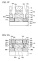
- Fig. 9G is the sectional view showing the semiconductor device that has been fabricated by the method of manufacturing the semiconductor device according to the second embodiment of the present invention.
- the semiconductor device has a dual damascene structure as shown in Fig. 9G.
- the device is made up of a lower wiring-buried insulating film 34 where lower wirings (38a, 38b) are buried, an upper wiring-buried insulating film 45 where upper wirings (55a, 55b) are buried, and a wiring interlayer insulating film 42 being sandwiched therebetween, where are laminated on a substrate 31.
- connecting conductors (54a, 54b) that connect the lower wirings (38a, 38b) with the upper wirings (55a, 55b) are buried.
- the lower wirings (38a, 38b), the connecting conductors (54a, 54b), and the upper wirings (55a, 55b) are mainly made of copper film.
- the lower wiring-buried insulating film 34 is made up of a primary insulating film and a barrier insulating film thereon
- the wiring interlayer insulating film 42 is made up of a lower barrier insulating, film, a primary insulating film, and an upper barrier insulating film
- the upper-wiring buried insulating film 45 is made up of a primary insulating film and a barrier insulating film thereon.
- the deposition condition I are applied for the deposition of each primary insulating film of the lower wiring-buried insulating film 34, the wiring interlayer insulating film 42, and the upper-wiring buried insulating film 45.
- the substrate 31 is carried into the chamber 1 of a deposition apparatus 101 first, and is held on a substrate holder 3. Subsequently, the substrate 31 is heated and maintained at the temperature of 350°C. Then, as shown in Fig. 9A, OMCTS, HMDSO, H 2 O, and He are introduced into the chamber 1 of the plasma deposition apparatus 101 shown in Fig. 1 at the flow rate of 75 sccm, 75 sccm, 500 sccm, and 100 sccm, respectively, and the pressure is held at 1.7 Torr.
- high-frequency power of 562W (equivalent to about 0.6W/cm 2 ) having the frequency of 13.56MHz is applied to the upper electrode 2.
- low-frequency power of 380kHz is not applied to the lower electrode 3.
- the SiOCH film is an insulating film containing Si, O, C, and H therein.
- a barrier insulating film 33 that constitutes the lower wiring-buried insulating film 34 is formed on the primary insulating film 32 by the plasma-enhanced CVD method.
- a silicon oxide film deposited by other deposition condition can be used representatively, and a silicon oxynitride film or a silicon nitride film can be also used. These films are a little higher in relative dielectric constant, but are higher in copper diffusion preventing function and mechanical strength. The same also applies to the barrier insulating film to be deposited as follows.
- a TaN film as a copper diffusion preventing film is formed on the inner surface of the lower wiring grooves (34a, 34b) as shown in Fig. 9C.
- a copper seed layer (not shown) has been formed on the surface of the TaN film by a sputtering method
- the copper film is buried by a plating method.
- the copper film and the TaN film that are protruded from the wiring grooves (34a, 34b) are polished by a CMP method (Chemical Mechanical Polishing method) to make the surface flat. Consequently, the lower wirings (38a, 38b) mainly made of copper film, which is made up of copper films (37a, 37b) and TaN films (36a, 36b), are formed.
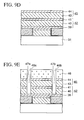
- the wiring interlayer insulating film 42 and the wiring-buried insulating film 45 are formed on the lower wiring-buried insulating film 34 shown in Fig. 9C. Its detail will be described as follows.
- the substrate 31 shown in Fig. 9C is carried into the chamber 1 of the deposition apparatus 101 first, and held on the substrate holder 3. Subsequently, the substrate 31 is heated and maintained at the temperature of 350°C.
- the deposition gas is introduced into the chamber 1 to transform the gas into plasma, reaction is caused to form a barrier insulating film 39 having the film thickness of about 100nm, which contacts the lower wirings (38a, 38b) and covers the lower wirings (38a, 38b) and the lower wiring buried insulating film 34.
- a primary insulating film 40 made of SiOCH film having the film thickness of about 500nm is formed on the barrier insulating film 39 under the same deposition condition as the deposition condition of the primary insulating film 32 of Fig. 9A.
- a barrier insulating film 41 having the film thickness of about 100nm is formed on the primary insulating film 40 by the plasma-enhanced CVD method.
- the wiring interlayer insulating film 42 made up of the barrier insulating film 39, the primary insulating film 40, and the barrier insulating film 41 is formed.
- the upper wiring-buried insulating film 45 is formed on the wiring interlayer insulating film 42.
- a barrier insulating film 44 having the film thickness of about 100nm is formed on the primary insulating film 43 by the plasma-enhanced CVD method.
- the upper wiring-buried insulating film 45 made up of the primary insulating film 43 and the barrier insulating film 44 is formed.
- a resist mask 46 having openings (46a, 46b) above the lower wirings (38a, 38b) is formed on the barrier insulating film 44, which constitutes the upper wiring-buried insulating film 45, by an exposure method.
- etching is sequentially performed to the barrier insulating film 44, the primary insulating film 43, the barrier insulating film 41, and the primary insulating film 40 through the openings (46a, 46b) to form openings (47a, 47b) reaching the barrier insulating film 39.
- a new resist mask 48 having openings (48a, 48b) is formed on the barrier insulating film 44 that constitutes the upper wiring-buried insulating film 45 by the exposure method.
- the openings (48a, 48b) of the resist mask 48 are formed so as to have wider opening width than the openings (47a, 47b) and include the openings (47a, 47b) inside thereof.
- the barrier insulating film 44 and the primary insulating film 43 which are exposed around the openings (47a, 47b) in the openings (48a, 48b), are sequentially etched through the openings (48a, 48b).
- reference numerals 50a and 50b in the drawing denote openings having the same shape and dimensions as the openings (47a, 47b).
- a TaN film as the copper diffusion preventing film is formed on the inner surface of the wiring connecting holes (51a, 51b) and the upper wiring grooves (49a, 49b). Then, after a copper seed layer (not shown) has been formed on the surface of the TaN film by the sputtering method, the copper film is buried by the plating method. Subsequently, the copper film and the TaN film protruded from the upper wiring grooves (49a, 49b) are polished by the CMP method to make the surface flat.
- a barrier insulating film 56 is formed on the entire surface. Thus, the semiconductor device is completed.
- each primary insulating film (32, 40, 43) of the lower wiring buried insulating film 34, the wiring interlayer insulating film 42, and the upper wiring buried insulating film 45 is deposited by the plasma-enhanced CVD method using deposition gas composing of gas mixture, where OMCTS (cyclic siloxane) having methyl group and HMDSO (chain siloxane) having methyl group are combined, and H 2 O (oxidizing gas) and He (diluting gas) which are further added to the gas mixture.
- OMCTS cyclic siloxane
- HMDSO chain siloxane
- inert gas as the diluting gas
- rapid reaction of deposition gas can be suppressed and vapor phase reaction can be suppressed. This prevents the reduction of the mechanical strength and adhesion strength of the formed film, and also prevents the generation of particles.
- it is preferable to add an appropriate amount of the inert gas because too much addition of the inert gas results in increase of the relative dielectric constant.
- the deposition condition I are used as the deposition condition for the primary insulating films (32, 40, 43), but the deposition condition II or other deposition condition surveyed in the first embodiment may be used.
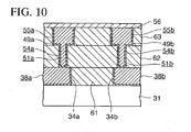
- Fig. 10 is the sectional view showing the semiconductor device being the third embodiment.
- a different point from Fig. 9G is that the lower wiring-buried insulating film 34, the wiring interlayer insulating film 42, and the upper wiring-buried insulating film 45 do not include the barrier insulating films 33, 39, 41, 44, respectively, and those compose of only primary insulating films (61, 62, 63), respectively.
- components in Fig. 10 shown by the same reference numerals as the reference numerals in Figs. 9A to 9G have the same functions as those of the components in Figs. 9A to 9G or denote the same components as the ones in Figs. 9A to 9G.
- the semiconductor device shown in Fig. 12 of the third embodiment has a structure where the barrier insulating films have been removed respectively from the lower wiring-buried insulating film 34, the wiring interlayer insulating film 42, and the upper wiring buried insulating film 45 of the semiconductor device shown in Fig. 9G.
- the deposition process of the barrier insulating films is omitted from the manufacturing method of the second embodiment.
- the deposition condition I or the deposition condition II of the second embodiment, or other deposition condition surveyed in the first embodiment can be applied as the deposition condition of the insulating films (61, 62, 63).
- each insulating film (61, 62, 63) be a film thickness as required for the lower wiring-buried insulating film 34, the wiring interlayer insulating film 42, and the upper wiring-buried insulating film 45.
- the single layer insulating films (61, 62, 63) constituting the lower wiring-buried insulating film 34, the wiring interlayer insulating film 42, and the upper wiring-buried insulating film 45 are deposited respectively by the plasma-enhanced CVD method using deposition gas that contains gas mixture where the cyclic siloxane having methyl group and the chain siloxane or organic silane having methyl group are combined as the silicon containing organic compound.
- the white turbidity of the formed primary insulating film (61, 62, 63) it is possible to prevent the white turbidity of the formed primary insulating film (61, 62, 63) to increase the mechanical strength, to improve the absorbing characteristic of the formed films, and to maintain the relative dielectric constant of the primary insulating films (61, 62, 63) as low as 2.6 or less, similar to the first embodiment. Consequently, high-speed performance of the semiconductor device can be improved. Furthermore, since the formed insulating films (61, 62, 63) have the copper diffusion preventing function, they are primary insulating films having low dielectric constant and also serve as the barrier insulating films to copper.
- the single layer insulating films (61, 62, 63) are available as the lower wiring-buried insulating film 34, the wiring interlayer insulating film 42, and the upper wiring-buried insulating film 45, and thus the deposition of the barrier insulating films can be omitted. As a result, the manufacturing process can be simplified.
- Fig. 11 is the sectional view showing the semiconductor device being the fourth embodiment. Note that components in Fig. 11 shown by the same reference numerals as the reference numerals in Figs. 9A to 9G have the same functions as those of the components in Figs. 9A to 9G or denote the same components as the ones in Figs. 9A to 9G.
- the semiconductor device being the fourth embodiment has the same laminated structure as the semiconductor device shown in Fig. 9G being the second embodiment.
- the semiconductor device has the dual damascene structure as shown in Fig. 11, and the dual damascene structure is made up of the lower wiring-buried insulating film 34 in which the lower wirings (38a, 38b) are buried, the upper wiring-buried insulating film 45 in which the upper wirings (55a, 55b) are buried, and the wiring interlayer insulating film 42 being sandwiched therebetween, in which the connecting conductors (54a, 54b) for connecting the lower wirings (38a, 38b) with the upper wirings (55a, 55b) are buried, on the substrate 31.
- the lower wirings (38a, 38b), the connecting conductors (54a, 54b), and the upper wirings (55a, 55b) are mainly made of copper film.
- the lower wiring-buried insulating film 34 is made up of a primary insulating film 64 and a barrier insulating film 65 thereon
- the wiring interlayer insulating film 42 is made up of a lower barrier insulating film 66, a primary insulating film 67, and an upper barrier insulating film 68
- the upper wiring-buried insulating film 45 is made up of a primary insulating film 69 and a barrier insulating film 70 thereon.
- the deposition condition I, the deposition condition II of this embodiment or other deposition condition surveyed in the first embodiment are used for the deposition of respective barrier insulating films (65, 66, 68, 70, 71) that severally belong to the lower wiring-buried insulating film 34, the wiring interlayer insulating film 42, and the upper wiring-buried insulating film 45, unlike the second embodiment.
- insulating films having much lower dielectric constant can be used as the primary insulating films (64, 67, 69).
- a porous insulating film formed by a series of processes of the deposition of the CVD method and post-treatment such as heating where the formed film is transformed into porous, or a coating insulating film formed by a coating method can be used.
- respective barrier insulating films (65, 66, 68, 70, 71) constituting the lower wiring buried insulating film 34, the wiring interlayer insulating film 42, and the upper wiring buried insulating film 45 are deposited by the plasma-enhanced CVD method using deposition gas that contains gas mixture where the cyclic siloxane having methyl group and the chain siloxane or organic silane having methyl group are combined as the silicon containing organic compound.
- the primary insulating films can lead to further reducing the relative dielectric constant of the lower wiring-buried insulating film 34, the wiring interlayer insulating film 42, and the upper wiring-buried insulating film 45. Consequently, high-speed performance of the semiconductor device can be improved.
- the present invention by performing deposition by the plasma-enhanced CVD method using deposition gas having gas mixture as primary constituent gas, in which cyclic siloxane having at least one of methyl group and methoxy group is combined with chain siloxane having at least one of methyl group and methoxy group, deposition gas having gas mixture as primary constituent gas, in which cyclic siloxane having at least one of methyl group and methoxy group is combined with organic silane having at least one of methyl group and methoxy group, or deposition gas in which oxidizing gas such as H 2 O is added to the gas mixture, the white turbidity of the insulating film to be formed is prevented to increase the mechanical strength, the absorbing characteristic is improved, and the relative dielectric constant of 2.6 or less can be maintained while the copper diffusion preventing function is maintained.
- This deposition method is applied for the semiconductor device on which copper wirings and the like are formed, and the insulating films having the above-described property can be used as the barrier insulating film covering the copper wirings or the like, as the insulating film directly covering the copper wirings or the like, or as the primary insulating film on the barrier insulating film covering the copper wirings or the like. Furthermore, it is also possible to use the above-described insulating film, the barrier insulating film, and the primary insulating film as insulating films constituting the wiring interlayer insulating film or the wiring-buried insulating film.
- the semiconductor device can follow the driving frequency exceeding GHz and the dimension of wiring pattern of 65nm or less without reducing the performance of the semiconductor device.
Landscapes
- Chemical & Material Sciences (AREA)
- Engineering & Computer Science (AREA)
- Materials Engineering (AREA)
- Organic Chemistry (AREA)
- Chemical Kinetics & Catalysis (AREA)
- Metallurgy (AREA)
- Mechanical Engineering (AREA)
- General Chemical & Material Sciences (AREA)
- Wood Science & Technology (AREA)
- Inorganic Chemistry (AREA)
- Life Sciences & Earth Sciences (AREA)
- Physics & Mathematics (AREA)
- Plasma & Fusion (AREA)
- Formation Of Insulating Films (AREA)
- Internal Circuitry In Semiconductor Integrated Circuit Devices (AREA)
- Chemical Vapour Deposition (AREA)
Applications Claiming Priority (2)
| Application Number | Priority Date | Filing Date | Title |
|---|---|---|---|
| JP2004103466A JP2005294333A (ja) | 2004-03-31 | 2004-03-31 | 成膜方法及び半導体装置 |
| JP2004103466 | 2004-03-31 |
Publications (2)
| Publication Number | Publication Date |
|---|---|
| EP1583142A2 true EP1583142A2 (fr) | 2005-10-05 |
| EP1583142A3 EP1583142A3 (fr) | 2007-05-02 |
Family
ID=34880034
Family Applications (1)
| Application Number | Title | Priority Date | Filing Date |
|---|---|---|---|
| EP05007007A Withdrawn EP1583142A3 (fr) | 2004-03-31 | 2005-03-31 | Procédé de déposition d'une couche isolante et dispositif semiconducteur |
Country Status (6)
| Country | Link |
|---|---|
| US (1) | US20050221622A1 (fr) |
| EP (1) | EP1583142A3 (fr) |
| JP (1) | JP2005294333A (fr) |
| KR (1) | KR100658479B1 (fr) |
| CN (1) | CN100347831C (fr) |
| TW (1) | TW200537644A (fr) |
Cited By (2)
| Publication number | Priority date | Publication date | Assignee | Title |
|---|---|---|---|---|
| EP1845100A4 (fr) * | 2005-01-31 | 2010-06-02 | Tosoh Corp | Compose siloxane cyclique, materiau filmogene contenant du silicium et utilisation de ce materiau |
| WO2022087151A1 (fr) * | 2020-10-20 | 2022-04-28 | Versum Materials Us, Llc | Alcoxydisiloxanes et films d'organosilicium denses fabriqués à partir de ceux-ci |
Families Citing this family (17)
| Publication number | Priority date | Publication date | Assignee | Title |
|---|---|---|---|---|
| JP3616605B2 (ja) * | 2002-04-03 | 2005-02-02 | 沖電気工業株式会社 | 半導体装置 |
| JP4656147B2 (ja) | 2005-09-13 | 2011-03-23 | 日本電気株式会社 | 多孔質絶縁膜の形成方法および半導体装置 |
| US8080282B2 (en) * | 2006-08-08 | 2011-12-20 | Asm Japan K.K. | Method for forming silicon carbide film containing oxygen |
| CN101611043B (zh) * | 2007-02-14 | 2013-03-13 | Jsr株式会社 | 含硅膜形成用材料、以及含硅绝缘膜及其形成方法 |
| US8637396B2 (en) * | 2008-12-01 | 2014-01-28 | Air Products And Chemicals, Inc. | Dielectric barrier deposition using oxygen containing precursor |
| US9330974B2 (en) * | 2010-10-27 | 2016-05-03 | Infineon Technologies Ag | Through level vias and methods of formation thereof |
| JP5946361B2 (ja) * | 2011-11-30 | 2016-07-06 | 株式会社Adeka | 1,3−ジフルオロジシロキサン化合物の製造方法 |
| CN103130825B (zh) * | 2011-11-30 | 2016-12-21 | 株式会社艾迪科 | 1,3‑二氟二硅氧烷化合物的制造方法 |
| KR102113605B1 (ko) * | 2013-07-26 | 2020-05-22 | 엘지디스플레이 주식회사 | 유기 발광 다이오드 표시 장치의 제조 방법 |
| CN104752633A (zh) * | 2013-12-31 | 2015-07-01 | 中国科学院微电子研究所 | 一种薄膜封装方法 |
| US10262892B2 (en) * | 2016-11-08 | 2019-04-16 | Globalfoundries Inc. | Skip via structures |
| WO2020046980A1 (fr) * | 2018-08-29 | 2020-03-05 | Applied Materials, Inc. | Dépôt d'un film anti-uv à faible k et d'une grande dureté |
| CN110828578B (zh) * | 2019-10-16 | 2022-11-08 | Tcl华星光电技术有限公司 | 薄膜晶体管及其制备方法与显示装置 |
| CN112779519A (zh) * | 2019-11-11 | 2021-05-11 | 夏泰鑫半导体(青岛)有限公司 | 低介电常数的氧化硅膜层及其制备方法及半导体元器件 |
| JP7611361B2 (ja) * | 2020-07-24 | 2025-01-09 | バーサム マテリアルズ ユーエス,リミティド ライアビリティ カンパニー | 環状シロキサン、及びこれを用いて製造された膜 |
| JP7689434B2 (ja) * | 2021-03-29 | 2025-06-06 | 東ソー株式会社 | ジヒドロジシロキサン化合物及びその製造方法 |
| JPWO2022230944A1 (fr) * | 2021-04-29 | 2022-11-03 |
Family Cites Families (24)
| Publication number | Priority date | Publication date | Assignee | Title |
|---|---|---|---|---|
| US5395908A (en) * | 1994-06-20 | 1995-03-07 | Dow Corning Corporation | Method of preparing in situ reinforced silicone elastomer |
| US7064088B2 (en) * | 1998-02-05 | 2006-06-20 | Asm Japan K.K. | Method for forming low-k hard film |
| US6593247B1 (en) * | 1998-02-11 | 2003-07-15 | Applied Materials, Inc. | Method of depositing low k films using an oxidizing plasma |
| US6068884A (en) * | 1998-04-28 | 2000-05-30 | Silcon Valley Group Thermal Systems, Llc | Method of making low κ dielectric inorganic/organic hybrid films |
| JP3600507B2 (ja) * | 2000-05-18 | 2004-12-15 | キヤノン販売株式会社 | 半導体装置及びその製造方法 |
| JP2002009069A (ja) * | 2000-06-22 | 2002-01-11 | Canon Sales Co Inc | 成膜方法 |
| US6835669B2 (en) * | 2000-07-21 | 2004-12-28 | Canon Sales Co., Inc. | Film forming method, semiconductor device and semiconductor device manufacturing method |
| TW531802B (en) * | 2000-07-21 | 2003-05-11 | Canon Sales Co Ltd | Semiconductor device and semiconductor device manufacturing method |
| US6500752B2 (en) * | 2000-07-21 | 2002-12-31 | Canon Sales Co., Inc. | Semiconductor device and semiconductor device manufacturing method |
| JP4167388B2 (ja) * | 2000-09-27 | 2008-10-15 | 株式会社東芝 | 半導体装置の製造方法 |
| JP3516941B2 (ja) * | 2000-11-30 | 2004-04-05 | キヤノン販売株式会社 | 半導体装置及びその製造方法 |
| KR100392840B1 (ko) * | 2000-12-02 | 2003-07-28 | 주식회사 우광케미칼 | 저온 플라즈마 중합법을 이용한 중합박막의 형성방법 |
| JP3545364B2 (ja) * | 2000-12-19 | 2004-07-21 | キヤノン販売株式会社 | 半導体装置及びその製造方法 |
| US6486082B1 (en) * | 2001-06-18 | 2002-11-26 | Applied Materials, Inc. | CVD plasma assisted lower dielectric constant sicoh film |
| JP3745257B2 (ja) * | 2001-08-17 | 2006-02-15 | キヤノン販売株式会社 | 半導体装置及びその製造方法 |
| JP4152619B2 (ja) * | 2001-11-14 | 2008-09-17 | 株式会社ルネサステクノロジ | 半導体装置およびその製造方法 |
| US6890850B2 (en) * | 2001-12-14 | 2005-05-10 | Applied Materials, Inc. | Method of depositing dielectric materials in damascene applications |
| US20030194495A1 (en) * | 2002-04-11 | 2003-10-16 | Applied Materials, Inc. | Crosslink cyclo-siloxane compound with linear bridging group to form ultra low k dielectric |
| US20030211244A1 (en) * | 2002-04-11 | 2003-11-13 | Applied Materials, Inc. | Reacting an organosilicon compound with an oxidizing gas to form an ultra low k dielectric |
| EP1504138A2 (fr) * | 2002-05-08 | 2005-02-09 | Applied Materials, Inc. | Procede de traitement de couche de constante dielectrique par faisceau electronique |
| JP4217870B2 (ja) * | 2002-07-15 | 2009-02-04 | 日本電気株式会社 | 有機シロキサン共重合体膜、その製造方法、成長装置、ならびに該共重合体膜を用いた半導体装置 |
| EP1573086A4 (fr) * | 2002-09-18 | 2012-10-03 | Air Prod & Chem | Additifs permettant d'empecher la deterioration des siloxanes d'alkyl-hydrogene |
| JP4032044B2 (ja) * | 2003-06-17 | 2008-01-16 | 株式会社半導体プロセス研究所 | 成膜方法、半導体装置の製造方法及び半導体装置 |
| JP3984611B2 (ja) * | 2004-02-13 | 2007-10-03 | 松下電器産業株式会社 | 有機無機ハイブリッド絶縁膜の形成方法 |
-
2004
- 2004-03-31 JP JP2004103466A patent/JP2005294333A/ja active Pending
-
2005
- 2005-03-28 US US11/090,272 patent/US20050221622A1/en not_active Abandoned
- 2005-03-28 TW TW094109544A patent/TW200537644A/zh unknown
- 2005-03-30 KR KR1020050026389A patent/KR100658479B1/ko not_active Expired - Fee Related
- 2005-03-30 CN CNB2005100625210A patent/CN100347831C/zh not_active Expired - Fee Related
- 2005-03-31 EP EP05007007A patent/EP1583142A3/fr not_active Withdrawn
Cited By (3)
| Publication number | Priority date | Publication date | Assignee | Title |
|---|---|---|---|---|
| EP1845100A4 (fr) * | 2005-01-31 | 2010-06-02 | Tosoh Corp | Compose siloxane cyclique, materiau filmogene contenant du silicium et utilisation de ce materiau |
| US8513448B2 (en) | 2005-01-31 | 2013-08-20 | Tosoh Corporation | Cyclic siloxane compound, a material for forming Si-containing film, and its use |
| WO2022087151A1 (fr) * | 2020-10-20 | 2022-04-28 | Versum Materials Us, Llc | Alcoxydisiloxanes et films d'organosilicium denses fabriqués à partir de ceux-ci |
Also Published As
| Publication number | Publication date |
|---|---|
| KR20060044992A (ko) | 2006-05-16 |
| JP2005294333A (ja) | 2005-10-20 |
| EP1583142A3 (fr) | 2007-05-02 |
| US20050221622A1 (en) | 2005-10-06 |
| TW200537644A (en) | 2005-11-16 |
| KR100658479B1 (ko) | 2006-12-19 |
| CN1677625A (zh) | 2005-10-05 |
| CN100347831C (zh) | 2007-11-07 |
Similar Documents
| Publication | Publication Date | Title |
|---|---|---|
| EP1583142A2 (fr) | Procédé de déposition d'une couche isolante et dispositif semiconducteur | |
| US6479409B2 (en) | Fabrication of a semiconductor device with an interlayer insulating film formed from a plasma devoid of an oxidizing agent | |
| US6649495B2 (en) | Manufacturing method of semiconductor device | |
| US8669181B1 (en) | Diffusion barrier and etch stop films | |
| CN102232125B (zh) | 使用含氧前体的介电阻挡层沉积 | |
| US6632478B2 (en) | Process for forming a low dielectric constant carbon-containing film | |
| CN101886255B (zh) | 使用含氮前体的介电阻挡层沉积 | |
| EP1217648A2 (fr) | Méthode de formation d'une couche diélectrique intermédiaire à constante diélectrique faible | |
| US20050059258A1 (en) | Structures with improved interfacial strength of SiCOH dielectrics and method for preparing the same | |
| KR100746679B1 (ko) | 성막 방법, 반도체 장치의 제조 방법 및 반도체 장치 | |
| US20020137323A1 (en) | Metal ion diffusion barrier layers | |
| KR100399633B1 (ko) | 반도체 장치 및 그 제조 방법 | |
| US20070237970A1 (en) | Diffusion barrier with low dielectric constant and semiconductor device containing same | |
| US6630412B2 (en) | Semiconductor device and method of manufacturing the same | |
| KR20020009440A (ko) | 성막 방법, 반도체 장치 및 그 제조 방법 | |
| KR101015534B1 (ko) | 저유전 상수를 갖는 절연막 및 이를 이용한 에어갭 제조 방법 | |
| EP1247876A2 (fr) | Procédé de fabrication d'un dispositif semiconducteur | |
| EP1128421A2 (fr) | Méthode de fabrication d'une d'une couche isolante intermédiaire contenant les éléments Si, C, O et H pour composants semiconducteurs | |
| JP2006339506A (ja) | 成膜方法及び半導体装置の製造方法 | |
| US20060115980A1 (en) | Method for decreasing a dielectric constant of a low-k film |
Legal Events
| Date | Code | Title | Description |
|---|---|---|---|
| PUAI | Public reference made under article 153(3) epc to a published international application that has entered the european phase |
Free format text: ORIGINAL CODE: 0009012 |
|
| AK | Designated contracting states |
Kind code of ref document: A2 Designated state(s): AT BE BG CH CY CZ DE DK EE ES FI FR GB GR HU IE IS IT LI LT LU MC NL PL PT RO SE SI SK TR |
|
| AX | Request for extension of the european patent |
Extension state: AL BA HR LV MK YU |
|
| PUAL | Search report despatched |
Free format text: ORIGINAL CODE: 0009013 |
|
| AK | Designated contracting states |
Kind code of ref document: A3 Designated state(s): AT BE BG CH CY CZ DE DK EE ES FI FR GB GR HU IE IS IT LI LT LU MC NL PL PT RO SE SI SK TR |
|
| AX | Request for extension of the european patent |
Extension state: AL BA HR LV MK YU |
|
| RIC1 | Information provided on ipc code assigned before grant |
Ipc: C08G 77/00 20060101ALI20070328BHEP Ipc: C09D 4/00 20060101ALI20070328BHEP Ipc: H01L 21/768 20060101ALI20070328BHEP Ipc: H01L 21/316 20060101ALI20070328BHEP Ipc: H01L 21/312 20060101AFI20050715BHEP |
|
| AKX | Designation fees paid |
Designated state(s): BE DE GB |
|
| STAA | Information on the status of an ep patent application or granted ep patent |
Free format text: STATUS: THE APPLICATION IS DEEMED TO BE WITHDRAWN |
|
| 18D | Application deemed to be withdrawn |
Effective date: 20071001 |