EP1577699A2 - Panneau pour appareil éléctro-optique, procédé de fabrication, appareil électro-optique et appareil électronique - Google Patents
Panneau pour appareil éléctro-optique, procédé de fabrication, appareil électro-optique et appareil électronique Download PDFInfo
- Publication number
- EP1577699A2 EP1577699A2 EP05005366A EP05005366A EP1577699A2 EP 1577699 A2 EP1577699 A2 EP 1577699A2 EP 05005366 A EP05005366 A EP 05005366A EP 05005366 A EP05005366 A EP 05005366A EP 1577699 A2 EP1577699 A2 EP 1577699A2
- Authority
- EP
- European Patent Office
- Prior art keywords
- convex portions
- substrate
- wires
- electro
- optical apparatus
- Prior art date
- Legal status (The legal status is an assumption and is not a legal conclusion. Google has not performed a legal analysis and makes no representation as to the accuracy of the status listed.)
- Withdrawn
Links
Images


Classifications
-
- G—PHYSICS
- G02—OPTICS
- G02F—OPTICAL DEVICES OR ARRANGEMENTS FOR THE CONTROL OF LIGHT BY MODIFICATION OF THE OPTICAL PROPERTIES OF THE MEDIA OF THE ELEMENTS INVOLVED THEREIN; NON-LINEAR OPTICS; FREQUENCY-CHANGING OF LIGHT; OPTICAL LOGIC ELEMENTS; OPTICAL ANALOGUE/DIGITAL CONVERTERS
- G02F1/00—Devices or arrangements for the control of the intensity, colour, phase, polarisation or direction of light arriving from an independent light source, e.g. switching, gating or modulating; Non-linear optics
- G02F1/01—Devices or arrangements for the control of the intensity, colour, phase, polarisation or direction of light arriving from an independent light source, e.g. switching, gating or modulating; Non-linear optics for the control of the intensity, phase, polarisation or colour
- G02F1/13—Devices or arrangements for the control of the intensity, colour, phase, polarisation or direction of light arriving from an independent light source, e.g. switching, gating or modulating; Non-linear optics for the control of the intensity, phase, polarisation or colour based on liquid crystals, e.g. single liquid crystal display cells
- G02F1/133—Constructional arrangements; Operation of liquid crystal cells; Circuit arrangements
- G02F1/1333—Constructional arrangements; Manufacturing methods
- G02F1/1345—Conductors connecting electrodes to cell terminals
-
- G—PHYSICS
- G02—OPTICS
- G02F—OPTICAL DEVICES OR ARRANGEMENTS FOR THE CONTROL OF LIGHT BY MODIFICATION OF THE OPTICAL PROPERTIES OF THE MEDIA OF THE ELEMENTS INVOLVED THEREIN; NON-LINEAR OPTICS; FREQUENCY-CHANGING OF LIGHT; OPTICAL LOGIC ELEMENTS; OPTICAL ANALOGUE/DIGITAL CONVERTERS
- G02F1/00—Devices or arrangements for the control of the intensity, colour, phase, polarisation or direction of light arriving from an independent light source, e.g. switching, gating or modulating; Non-linear optics
- G02F1/01—Devices or arrangements for the control of the intensity, colour, phase, polarisation or direction of light arriving from an independent light source, e.g. switching, gating or modulating; Non-linear optics for the control of the intensity, phase, polarisation or colour
- G02F1/13—Devices or arrangements for the control of the intensity, colour, phase, polarisation or direction of light arriving from an independent light source, e.g. switching, gating or modulating; Non-linear optics for the control of the intensity, phase, polarisation or colour based on liquid crystals, e.g. single liquid crystal display cells
- G02F1/133—Constructional arrangements; Operation of liquid crystal cells; Circuit arrangements
- G02F1/136—Liquid crystal cells structurally associated with a semi-conducting layer or substrate, e.g. cells forming part of an integrated circuit
- G02F1/1362—Active matrix addressed cells
-
- G—PHYSICS
- G02—OPTICS
- G02F—OPTICAL DEVICES OR ARRANGEMENTS FOR THE CONTROL OF LIGHT BY MODIFICATION OF THE OPTICAL PROPERTIES OF THE MEDIA OF THE ELEMENTS INVOLVED THEREIN; NON-LINEAR OPTICS; FREQUENCY-CHANGING OF LIGHT; OPTICAL LOGIC ELEMENTS; OPTICAL ANALOGUE/DIGITAL CONVERTERS
- G02F1/00—Devices or arrangements for the control of the intensity, colour, phase, polarisation or direction of light arriving from an independent light source, e.g. switching, gating or modulating; Non-linear optics
- G02F1/01—Devices or arrangements for the control of the intensity, colour, phase, polarisation or direction of light arriving from an independent light source, e.g. switching, gating or modulating; Non-linear optics for the control of the intensity, phase, polarisation or colour
- G02F1/13—Devices or arrangements for the control of the intensity, colour, phase, polarisation or direction of light arriving from an independent light source, e.g. switching, gating or modulating; Non-linear optics for the control of the intensity, phase, polarisation or colour based on liquid crystals, e.g. single liquid crystal display cells
- G02F1/133—Constructional arrangements; Operation of liquid crystal cells; Circuit arrangements
- G02F1/1333—Constructional arrangements; Manufacturing methods
- G02F1/1345—Conductors connecting electrodes to cell terminals
- G02F1/13452—Conductors connecting driver circuitry and terminals of panels
-
- G—PHYSICS
- G02—OPTICS
- G02F—OPTICAL DEVICES OR ARRANGEMENTS FOR THE CONTROL OF LIGHT BY MODIFICATION OF THE OPTICAL PROPERTIES OF THE MEDIA OF THE ELEMENTS INVOLVED THEREIN; NON-LINEAR OPTICS; FREQUENCY-CHANGING OF LIGHT; OPTICAL LOGIC ELEMENTS; OPTICAL ANALOGUE/DIGITAL CONVERTERS
- G02F1/00—Devices or arrangements for the control of the intensity, colour, phase, polarisation or direction of light arriving from an independent light source, e.g. switching, gating or modulating; Non-linear optics
- G02F1/01—Devices or arrangements for the control of the intensity, colour, phase, polarisation or direction of light arriving from an independent light source, e.g. switching, gating or modulating; Non-linear optics for the control of the intensity, phase, polarisation or colour
- G02F1/13—Devices or arrangements for the control of the intensity, colour, phase, polarisation or direction of light arriving from an independent light source, e.g. switching, gating or modulating; Non-linear optics for the control of the intensity, phase, polarisation or colour based on liquid crystals, e.g. single liquid crystal display cells
- G02F1/133—Constructional arrangements; Operation of liquid crystal cells; Circuit arrangements
- G02F1/1333—Constructional arrangements; Manufacturing methods
- G02F1/1345—Conductors connecting electrodes to cell terminals
- G02F1/13458—Terminal pads
-
- H—ELECTRICITY
- H05—ELECTRIC TECHNIQUES NOT OTHERWISE PROVIDED FOR
- H05K—PRINTED CIRCUITS; CASINGS OR CONSTRUCTIONAL DETAILS OF ELECTRIC APPARATUS; MANUFACTURE OF ASSEMBLAGES OF ELECTRICAL COMPONENTS
- H05K3/00—Apparatus or processes for manufacturing printed circuits
- H05K3/40—Forming printed elements for providing electric connections to or between printed circuits
- H05K3/4007—Surface contacts, e.g. bumps
-
- G—PHYSICS
- G02—OPTICS
- G02F—OPTICAL DEVICES OR ARRANGEMENTS FOR THE CONTROL OF LIGHT BY MODIFICATION OF THE OPTICAL PROPERTIES OF THE MEDIA OF THE ELEMENTS INVOLVED THEREIN; NON-LINEAR OPTICS; FREQUENCY-CHANGING OF LIGHT; OPTICAL LOGIC ELEMENTS; OPTICAL ANALOGUE/DIGITAL CONVERTERS
- G02F1/00—Devices or arrangements for the control of the intensity, colour, phase, polarisation or direction of light arriving from an independent light source, e.g. switching, gating or modulating; Non-linear optics
- G02F1/01—Devices or arrangements for the control of the intensity, colour, phase, polarisation or direction of light arriving from an independent light source, e.g. switching, gating or modulating; Non-linear optics for the control of the intensity, phase, polarisation or colour
- G02F1/13—Devices or arrangements for the control of the intensity, colour, phase, polarisation or direction of light arriving from an independent light source, e.g. switching, gating or modulating; Non-linear optics for the control of the intensity, phase, polarisation or colour based on liquid crystals, e.g. single liquid crystal display cells
- G02F1/133—Constructional arrangements; Operation of liquid crystal cells; Circuit arrangements
- G02F1/136—Liquid crystal cells structurally associated with a semi-conducting layer or substrate, e.g. cells forming part of an integrated circuit
- G02F1/1362—Active matrix addressed cells
- G02F1/136277—Active matrix addressed cells formed on a semiconductor substrate, e.g. of silicon
-
- H—ELECTRICITY
- H05—ELECTRIC TECHNIQUES NOT OTHERWISE PROVIDED FOR
- H05K—PRINTED CIRCUITS; CASINGS OR CONSTRUCTIONAL DETAILS OF ELECTRIC APPARATUS; MANUFACTURE OF ASSEMBLAGES OF ELECTRICAL COMPONENTS
- H05K2201/00—Indexing scheme relating to printed circuits covered by H05K1/00
- H05K2201/03—Conductive materials
- H05K2201/0332—Structure of the conductor
- H05K2201/0364—Conductor shape
- H05K2201/0367—Metallic bump or raised conductor not used as solder bump
-
- H—ELECTRICITY
- H05—ELECTRIC TECHNIQUES NOT OTHERWISE PROVIDED FOR
- H05K—PRINTED CIRCUITS; CASINGS OR CONSTRUCTIONAL DETAILS OF ELECTRIC APPARATUS; MANUFACTURE OF ASSEMBLAGES OF ELECTRICAL COMPONENTS
- H05K2201/00—Indexing scheme relating to printed circuits covered by H05K1/00
- H05K2201/09—Shape and layout
- H05K2201/09818—Shape or layout details not covered by a single group of H05K2201/09009 - H05K2201/09809
- H05K2201/09909—Special local insulating pattern, e.g. as dam around component
-
- H—ELECTRICITY
- H05—ELECTRIC TECHNIQUES NOT OTHERWISE PROVIDED FOR
- H05K—PRINTED CIRCUITS; CASINGS OR CONSTRUCTIONAL DETAILS OF ELECTRIC APPARATUS; MANUFACTURE OF ASSEMBLAGES OF ELECTRICAL COMPONENTS
- H05K2203/00—Indexing scheme relating to apparatus or processes for manufacturing printed circuits covered by H05K3/00
- H05K2203/01—Tools for processing; Objects used during processing
- H05K2203/0104—Tools for processing; Objects used during processing for patterning or coating
- H05K2203/013—Inkjet printing, e.g. for printing insulating material or resist
-
- H—ELECTRICITY
- H05—ELECTRIC TECHNIQUES NOT OTHERWISE PROVIDED FOR
- H05K—PRINTED CIRCUITS; CASINGS OR CONSTRUCTIONAL DETAILS OF ELECTRIC APPARATUS; MANUFACTURE OF ASSEMBLAGES OF ELECTRICAL COMPONENTS
- H05K3/00—Apparatus or processes for manufacturing printed circuits
- H05K3/0011—Working of insulating substrates or insulating layers
- H05K3/0017—Etching of the substrate by chemical or physical means
- H05K3/0023—Etching of the substrate by chemical or physical means by exposure and development of a photosensitive insulating layer
-
- Y—GENERAL TAGGING OF NEW TECHNOLOGICAL DEVELOPMENTS; GENERAL TAGGING OF CROSS-SECTIONAL TECHNOLOGIES SPANNING OVER SEVERAL SECTIONS OF THE IPC; TECHNICAL SUBJECTS COVERED BY FORMER USPC CROSS-REFERENCE ART COLLECTIONS [XRACs] AND DIGESTS
- Y10—TECHNICAL SUBJECTS COVERED BY FORMER USPC
- Y10T—TECHNICAL SUBJECTS COVERED BY FORMER US CLASSIFICATION
- Y10T29/00—Metal working
- Y10T29/49—Method of mechanical manufacture
- Y10T29/49002—Electrical device making
- Y10T29/49117—Conductor or circuit manufacturing
- Y10T29/49124—On flat or curved insulated base, e.g., printed circuit, etc.
- Y10T29/49126—Assembling bases
-
- Y—GENERAL TAGGING OF NEW TECHNOLOGICAL DEVELOPMENTS; GENERAL TAGGING OF CROSS-SECTIONAL TECHNOLOGIES SPANNING OVER SEVERAL SECTIONS OF THE IPC; TECHNICAL SUBJECTS COVERED BY FORMER USPC CROSS-REFERENCE ART COLLECTIONS [XRACs] AND DIGESTS
- Y10—TECHNICAL SUBJECTS COVERED BY FORMER USPC
- Y10T—TECHNICAL SUBJECTS COVERED BY FORMER US CLASSIFICATION
- Y10T29/00—Metal working
- Y10T29/49—Method of mechanical manufacture
- Y10T29/49002—Electrical device making
- Y10T29/49117—Conductor or circuit manufacturing
- Y10T29/49124—On flat or curved insulated base, e.g., printed circuit, etc.
- Y10T29/4913—Assembling to base an electrical component, e.g., capacitor, etc.
-
- Y—GENERAL TAGGING OF NEW TECHNOLOGICAL DEVELOPMENTS; GENERAL TAGGING OF CROSS-SECTIONAL TECHNOLOGIES SPANNING OVER SEVERAL SECTIONS OF THE IPC; TECHNICAL SUBJECTS COVERED BY FORMER USPC CROSS-REFERENCE ART COLLECTIONS [XRACs] AND DIGESTS
- Y10—TECHNICAL SUBJECTS COVERED BY FORMER USPC
- Y10T—TECHNICAL SUBJECTS COVERED BY FORMER US CLASSIFICATION
- Y10T29/00—Metal working
- Y10T29/49—Method of mechanical manufacture
- Y10T29/49002—Electrical device making
- Y10T29/49117—Conductor or circuit manufacturing
- Y10T29/49124—On flat or curved insulated base, e.g., printed circuit, etc.
- Y10T29/49155—Manufacturing circuit on or in base
Definitions
- the present invention relates to a panel for an electro-optical apparatus, a method of manufacture thereof, an electro-optical apparatus and an electronic apparatus.
- the Au bumps that are formed on the drive IC are expensive due to the fact that Au (i.e., gold) is used therefor.
- Au i.e., gold
- the pitch between electrodes of the drive IC has grown narrower, it is predicted that consistent bump formation such as the formation of high aspect resist or the etching of the seed layer and the like will become more difficult.
- wafer level CSP where manufacturing is performed at the wafer level.
- semiconductor elements whose wiring has a resin layer are formed in wafer units, and semiconductor devices are then formed by cutting each semiconductor element.
- non-electrolytic Ni bumps are harder than Au bumps
- COG chip on glass
- the protruding electrodes that are provided on the liquid crystal panel side are formed from glass. Therefore, in these protruding electrodes that are made of glass, when the drive IC is being packaged on the liquid crystal panel, in some cases, a thermal deformation such as stress or the like occurs on the liquid crystal panel or on the drive IC, and it is difficult for this deformation to be absorbed. As a result, malfunctions may occur when packaging electronic components.
- the present invention was conceived in view of the above described circumstances, and it is an object thereof to provide a panel for an electro-optical apparatus that enables the pitch between electrodes to be narrowed, and that also enables electrodes having a high degree of connection reliability to be manufactured, and to provide a method of manufacturing the panel for an electro-optical apparatus, and also to provide an electro-optical apparatus and a method of manufacturing the electro-optical apparatus, and to provide an electronic apparatus.
- the present invention is a panel for an electro-optical apparatus, has a substrate, a plurality of wires formed on the substrate, convex portions formed from resin and provided either on the plurality of wires or on the substrate, conductive layers provided so as to cover at least a portion of the surfaces of the convex portions, and that are electrically connected to the respective wires, and a plurality of external connection terminals for electrically connecting electronic components, formed by the convex portions and the conductive layers.
- convex portions that are made of resin are provided on a substrate, it is not necessary to form electrolytic Au bumps, which are high-cost, conductive protruding portions, on connection terminals of an electronic component that is being packaged on the substrate.
- electrolytic Au bumps which are high-cost, conductive protruding portions
- connection terminals of an electronic component that is being packaged on the substrate there are cases in which heat deformation such as stress is generated in the substrate or electronic component by heating or pressure.
- convex portions that are made of resin are provided on the substrate, when the electronic component is being packaged on the substrate, it is possible to absorb stress from the electronic component or panel. As a result, malfunctions in the packaging of the electronic component can be avoided.
- the present invention is a panel for an electro-optical apparatus, has a substrate, convex portions formed from resin and provided on the substrate, a plurality of wires provided on the substrate so as to cover at least a portion of the surfaces of the convex portions, and a plurality of external connection terminals for electrically connecting electronic components, formed by the convex portions and the wires.
- the convex portions prefferably be formed separated from each other with one convex portion formed for each external connection terminal.
- the convex portions may be formed a continuous convex portion extending over a plurality of mutually adjacent external connection terminals.
- the convex portion can be formed without any narrowing in pitch needing to be considered.
- a height of the continuous convex portion is lower at a portion located between adjacent external connection terminals than at the external connection terminals.
- the present invention is a method of manufacturing a panel for an electro-optical apparatus, has the steps of forming a plurality of wires on a substrate, forming convex portions composed of resin, either on the plurality of wires or on the substrate, forming conductive layers that are electrically connected to the respective wires so as to cover at least a portion of the surfaces of the convex portions, and forming a plurality of external connection terminals for electrically connecting electronic components by the convex portions and the conductive layers.
- the present invention is a method of manufacturing a panel for an electro-optical apparatus, has the steps of forming convex portions that are composed of resin on a substrate, forming a plurality of wires on the substrate so as to cover at least a portion of the surfaces of the convex portions, and forming a plurality of external connection terminals for electrically connecting electronic components by the convex portions and the wires.
- the wires also perform the functions of a conductive layer, the wires and conductive layer can be formed in a single step. As a result, a reduction in the number of manufacturing steps can be achieved.
- the resin be a photosensitive resin, and that the convex portions be formed by a photolithographic method.
- the convex portions can be formed accurately and with a high degree of precision in predetermined positions on the substrate. Moreover, by controlling the exposure, developing, or curing conditions, smooth, hemispherical convex portions can be formed.
- the convex portions may be formed by a droplet discharge method.
- droplets of liquid material can be accurately discharged onto predetermined positions, and convex portions can be formed using the minimum amount of droplets of liquid material that is necessary.
- the conductive layers or the wires may be formed by a droplet discharge method.
- droplets of liquid material can be accurately discharged onto predetermined positions, and a conductive layer or wires can be formed using the minimum amount of droplets of liquid material that is necessary.
- the electro-optical apparatus of the present invention is an electro-optical apparatus in which an electronic component is packaged via an adhesive agent on the external connection terminals of the above described panel for an electro-optical apparatus.
- non-electrolytic Ni bumps it is also possible for non-electrolytic Ni bumps to be formed on an electrode surface of the electronic component.
- the electrodes are formed so as to protrude beyond electrodes normally provided on an electronic component, it is possible to improve the connection reliability between these electrodes and external connection terminals when this electronic component is packaged on a substrate. Moreover, because they are formed so as to cover the top portions of A1 electrodes, corrosion of the electrodes can be prevented.
- the adhesive agent may not contain conductive particles.
- the adhesive agent does not contain conductive particles, a reduction in costs can be achieved compared with when the adhesive agent does contain conductive particles. In addition, short-circuiting malfunctions between external connection terminals can be prevented.
- the electronic apparatus of the present invention is provided with the above described electro-optical apparatus.
- an electronic apparatus can be provided that has an excellent display quality.
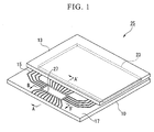
- FIG. 1 is a perspective view showing the schematic structure of a liquid crystal panel 25 (i.e., a panel for an electro-optical apparatus) of the present embodiment.
- a first substrate 10 i.e., a substrate
- a second substrate 13 are bonded by an ultraviolet light-cured sealing material 23. Liquid crystal is sealed and held inside an area surrounded by this sealing material 23.
- the liquid crystal panel 25 is provided with a plurality of wires 15 that are formed in a predetermined pattern on the first substrate 10, convex portions 19 that are formed on top of the wires 15, and conductive layers 21 that are formed on top of the convex portions 19.
- illumination devices such as backlights and other accessory equipment are also provided for the liquid crystal panel 25.
- the first substrate 10 is formed from soda glass and a transparent electrode layer is formed on top of this substrate.
- the thickness of the first substrate is, for example, 0.7 mm.
- the second substrate 13 is also formed from soda glass, and a transparent electrode layer is formed on top of this substrate.
- the thickness of the second substrate is, for example, 0.7 mm.
- the substrate that is used for the first substrate 10 has a larger outer configuration than that of the substrate that is used for the second substrate 13. Accordingly, when this pair of substrates are adhered together, edges (i.e., end surfaces of the substrate) of three sides of the two substrates (i.e., the top side, the right side, and the left side in FIG. 1) are substantially aligned, however, a peripheral portion of the first substrate 10 protrudes beyond the remaining side (i.e., the bottom side in FIG. 1) of the second substrate 13. In the present embodiment, the protruding peripheral portion of the first substrate 10 is called a protruding area 17.
- a plurality of pixel electrodes are formed on the joining surface side of the first substrate 10 (except for on the protruding area 17).
- striped electrodes in the form of thin strips are formed on the joining surface side of the second substrate 13.
- Oriented films are further formed on inner surface sides of each of the electrodes that are formed on the first substrate 10 and the second substrate 13.
- a thin film transistor (TFT) or the like is formed as a switching element on each pixel electrode of the first substrate 10.
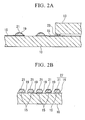
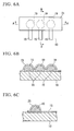
- FIG. 2A is a cross-sectional view taken along a line A-A' of the protruding area 17 of the first substrate 10 in the present embodiment.
- FIG. 2B is a cross-sectional view taken along a line B-B' of the protruding area 17 of the first substrate 10.
- a plurality of wires 15 are formed in a predetermined pattern on the protruding area 17.
- the convex portions 19 are formed on one end of each wire 15.
- the conductive layers 21 are formed on each of the convex portions 19.
- a plurality of the wires 15 are formed in a predetermined pattern on the first substrate 10.
- One end of each of the plurality of wires 15 that are formed in a predetermined pattern is formed so as to correspond to a packaging position of an electrode of a liquid crystal drive IC 30 (i.e., an electronic component) that is to be packaged on the first substrate 10.
- a plurality of electrodes of the liquid crystal drive IC 30, which is formed in a rectangular shape are formed with a uniform space between each along each of two mutually parallel sides that run in the longitudinal direction of the rectangular shape.
- a plurality of these electrodes are formed with a uniform space between each along each of two mutually parallel sides that run in the transverse direction of the rectangular shape. Accordingly, as shown in FIG. 1, one end of each of the plurality of wires 15 is formed so as to be located in a position, or near to a position where an electrode of the liquid crystal drive IC 30 is to be packaged.
- ITO Indium tin oxide
- a metal such as Ti, Cr, W, Ta, Mo, and Pb, or an alloy containing at least one of these can be used for the plurality of wires 15 that are formed in the predetermined pattern.
- the convex portions 19 are formed respectively on one end of the plurality of wires 15 that are formed in the predetermined pattern. Namely, the convex portions 19 are formed independently on each wire 15. The convex portions 19 are formed in a hemispherical shape, and the diameter of these hemispheres is larger than the width of the wire used for the wires 15. Note that the convex portions 19 are formed respectively on one end of the plurality of wires 15 that are formed in the predetermined pattern, however, it is preferable that the convex portions 19 be formed in the vicinity of the one end of the wires 15.
- the convex portions 19 are formed from resin. Specifically, they can be formed from resin such as a polyimide resin, a silicone modified polyimide resin, an epoxy resin, a silicone modified epoxy resin, benzocyclobutane (BCB), polybenzoxazole (PBO), phenol based resins, and acrylic based resins.
- resin such as a polyimide resin, a silicone modified polyimide resin, an epoxy resin, a silicone modified epoxy resin, benzocyclobutane (BCB), polybenzoxazole (PBO), phenol based resins, and acrylic based resins.
- the conductive layers 21 are formed so as to cover a portion of the surface of the convex portions 19 that are formed in a hemispherical shape on one end of each of the plurality of wires 15. Furthermore, the conductive layers 21 extend from the surface of the convex portions 19 to the top of the wires 15, and are electrically connected to the wires 15 via the convex portions 19.
- a metal such as Au, TiW, Cu, Cr, Ni, Ti, W, NiV, and A1 can be used for the conductive layers 21.
- the conductive layers 21 can also be formed by laminating these metals. Note that it is preferable that the conductive layers 21 (or at least one layer thereof in the case of a laminated structure) be formed using a metal, for example, Au, TiW, Cr that has a higher corrosion resistance than that of the electrodes. By using such a metal, corrosion of electrodes is prevented, and it is possible to prevent electrical malfunctions being generated.
- a plurality of external connection terminals 27 that are formed in this manner are formed on the protruding area 17 at positions where electrodes that are formed on the liquid crystal drive IC 30 are to be packaged.
- the liquid crystal drive IC 30 is packaged on the external connection terminals 27, so that the external connection terminals 27 and the electrodes that are formed on the liquid crystal drive IC 30 are electrically connected.
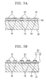
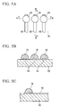
- FIG. 3A is a cross-sectional view taken across a line B-B' in FIG. 1 when the convex portions 19 are formed continuously so as to extend for a plurality of mutually adjacent external connection terminals 27.
- FIG. 3B is a cross-sectional view taken across a line B-B' in FIG. 1 in a case in which, among the convex portions 19 that are formed continuously so as to extend for plurality of mutually adjacent external connection terminals 27, the height between adjacent external connection terminals 27 is lower in portions than the height of the external connection terminals 27.
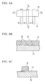
- FIGS. 4B, 5B, 6B, 7B and 8B are cross-sectional views taken along a line A-A in each of FIGS. 4A, 5A, 6A, 7A and 8A.
- FIGS. 4C, 5C, 6C, 7C and 8C are cross-sectional views taken along a line B-B in each of FIGS. 4A, 5A, 6A, 7A and 8A.
- a step of forming the wires 15, a step of forming the convex portions 19, and a step of forming the conductive layers 21 in the present embodiment will be described.
- a painting step in which the sealing material 23 is painted on the first substrate 10 a preliminary curing step to cure the painted sealing material 23, a liquid crystal placement step in which a liquid crystal 25 is placed in an area on the substrate that is surrounded by the sealing material 23, a step in which the respective substrates are adhered together via the sealing material 23, and a sealing material curing step in which the sealing material 23 is cured using ultraviolet light irradiation.
- a step for forming a TFT can be provided prior to the wire formation step, however, because a known step is used for forming the TFT and the like, a description thereof is omitted in the present embodiment.
- an alignment step is provided prior to the sealing material 23 painting step in which alignment marks are formed such that the sealing material 23 and the liquid crystal 25 can be painted or coated in predetermined positions, and the substrates are then positioned based on these alignment marks, however, here, a description of the alignment step is omitted.
- a silicon oxide film (SiO 2 ) is formed on a surface of the first substrate 10 using a chemical vapor deposition (CVD) method.
- the film thickness of this silicon oxide film is, for example, approximately 200 nm.
- the plurality of wires 15 are formed using a photolithographic method in a predetermined pattern on the first substrate 10.
- ITO or a simple metal substance, an alloy, or a metal silicide or the like containing at least one of Ti, Cr, W, Ta, Mo, and Pb is accumulated on the surface of the first substrate 10 including the protruding area 17 using a sputtering method, a CVD method, an electron beam thermal evaporation method or the like.
- resist is coated on this metal film using a spin coating method, a dipping method, a spray coating method or the like.
- a mask is then transferred in a predetermined pattern onto the resist using laser light or the like.
- the wires 15 that are formed on the protruding area 17 are formed in a predetermined pattern so as to correspond to the placement of the electrodes of the liquid crystal drive IC 30 that is being packaged. Next, exposure processing and developing processing are performed so that the resist is patterned in a predetermined configuration.
- the metal or the like that is placed in the area formed in a predetermined pattern where the resist has been removed by the aforementioned exposure processing and developing processing is etched. Namely, using the resist that is formed in a predetermined pattern as a mask, portions where the metal or the like is exposed are removed. Next, resist that is remaining on the metal or the like is peeled off. Note that the etching may be performed using any of a variety of methods such as dry etching, wet etching, or plasma etching.
- the wires 15 can be formed in a predetermined pattern.
- FIGS. 4A to 8C shown below are partial enlarged views showing a portion of the protruding area 17 in enlargement in order to simplify understanding of the steps for forming the convex portions 19 and the conductive layers 21.
- FIGS. 4A to 4C resin is coated on an area that includes at least one end of the plurality of wires 15 that are formed on the protruding area 17.
- exposure processing, developing processing, and curing processing are performed so that the convex portions 19 are formed in a hemispherical shape on one end of each of the wires 15 that are formed in a predetermined pattern.
- smooth, hemispherical convex portions 19 can be formed.
- a conductive layer 21 is formed on areas that include the wires 15 that have been formed using an aforementioned method and the convex portions 19 that have been formed on the wires 15.
- the conductive layer 21 is formed by a sputtering method or plating method over the entire surface including the wires 15 and the convex portions that are formed on the wires 15. Note that, if plating method is performed, the layer formed in the plating step constitutes the seed layer.
- resist 7 is coated on the entire surface of the above described conductive layer 21 using a method such as a spin coating method, a dipping method, a spray coating method or the like. After this, exposure processing and developing processing are performed, and a mask pattern in which apertures are formed that correspond to the planar shape (i.e., to the planar pattern) of the conductive layer 21 is transferred onto the conductive layer 21. The resist 7 is then patterned in a predetermined shape. Note that, if a plating method is used to form the conductive layer 21, then plating processing is performed on the seed layer on which the resist 7 is patterned.
- the sealing material 23 is painted on the first substrate 10.
- the sealing material 23 is painted in a closed toroidal configuration that does not include the liquid crystal injection apertures using a dispensing method, a printing method, and inkjet method or the like.
- the material used for the sealing material 23 is an epoxy based or acrylic based resin having viscosity, and a resin that can be cured by ultraviolet light or that can be cured by heat is used.
- a preliminary curing step is performed on the sealing material 23.
- the sealing material 23 is heated, for example, to a temperature of 80°C to 120°C for between 15 and 60 seconds using any of a variety of heating apparatuses such as a hot plate.
- the liquid crystal 25 is coated on the first substrate 10 within an area surrounded by the sealing material 23.
- Known technology such as an inkjet method can be used for the method of coating the liquid crystal 25.
- a TN type of STN type of material can be used for the liquid crystal material.
- the first substrate 10 and the second substrate 13 are adhered together via the already formed sealing material 23.
- the pressure that is applied during the adhesion is, for example, approximately 10 5 Pa.
- sealing material 23 is cured by ultraviolet light irradiation using a UV lamp.
- the ultraviolet light irradiation is performed in irradiation conditions of, for example, approximately 2000 mJ/cm 2 to 10000 mJ/cm 2 .
- the above described liquid crystal panel 25 can be manufactured by steps such as those described above.
- the convex portions 19 are formed using a photolithographic method, the convex portions 19 can be formed accurately and with a high degree of precision in predetermined positions on the first substrate 10. In addition, by controlling the exposure, developing and curing conditions, it is possible to form smooth, hemispherical convex portions 19.
- thin films are manufactured using a sputtering method, and these manufactured thin films are formed into wires 15, convex portions 19, and conductive layers 21 in a predetermined pattern using a photolithographic method.
- the wires 15, convex portions 19, and conductive layers 21 are formed using an inkjet method. A description is given below in detail of the structure of an inkjet apparatus and of a method of forming the wires 15, convex portions 19, and conductive layers 21.
- the painting step in which the sealing material 23 is painted on the first substrate 10 the preliminary curing step to cure the painted sealing material 23, the liquid crystal placement step in which the liquid crystal 25 is placed in an area on the substrate that is surrounded by the sealing material 23, the step in which the respective substrates are adhered together via the sealing material 23, and the sealing material curing step in which the sealing material 23 is cured using ultraviolet light irradiation are performed using the same methods as in the above described first embodiment, a description thereof is omitted here.
- FIG. 9 is a schematic perspective view of the inkjet apparatus 60 according to the present embodiment.
- the inkjet apparatus 60 is provided with an inkjet head group 41, an X direction guide shaft 42 that is used to drive the inkjet head group 41 in an X direction, and an X direction drive motor 43 that rotates the X direction guide shaft 42.
- the inkjet apparatus 60 is provided with a mounting base 44 on which a substrate 51 is mounted, a Y direction guide shaft 45 that is used to drive the mounting base 44 in a Y direction, and a Y direction drive motor 46 that rotates the Y direction guide shaft 45.
- a control unit 48 is provided underneath the base 47.
- a cleaning mechanism section 54 and a heater 55 are also provided.
- the inkjet head group 41 is provided with a plurality of inkjet heads that discharge a dispersion solution that contains fine conductive grains from nozzles (i.e., discharge apertures) and supply them to the substrate at predetermined spacings. It is possible for the dispersion solution to be discharged individually from each of the plurality of inkjet heads in accordance with a discharge voltage that is supplied from the control unit 48.
- the inkjet head group 41 is fixed to the X direction guide shaft 42, and the X direction drive motor 43 is connected to the X direction guide shaft 42.
- the X direction drive motor 43 is a stepping motor or the like. When the X direction drive motor 43 receives an X direction drive pulse signal from the control unit 48, it rotates the X direction guide shaft 42. When the X direction guide shaft 42 is rotated, the inkjet head group 41 moves in the X axial direction along the base 47.
- FIG. 10A and 10B are views showing an inkjet head 70.
- the inkjet head 70 is provided with a nozzle plate 72 formed from, for example, stainless steel and a diaphragm 73, and these two are joined together via a partitioning member (i.e., a reservoir plate) 74.
- a plurality of spaces 75 and a solution container 76 are formed by the partitioning members 74 between the nozzle plate 72 and the diaphragm 73.
- the interiors of each space 75 and of the solution container 76 are filled with a liquid, and the respective spaces 75 and the solution container 76 are connected together via supply ports 77.
- a plurality of nozzle holes 78 are formed in rows running in the vertical and horizontal directions in the nozzle plate 72, and the liquid is discharged from the spaces 75 via these nozzle holes 78.
- a hole 79 that is used to supply the liquid to the solution container 76 is formed in the diaphragm 73.
- a piezoelectric element 80 is joined onto the surface of the diaphragm 73 on the opposite side to the surface thereof that faces the spaces 75.
- This piezoelectric element 80 is positioned between a pair of electrodes 81, and a structure is employed in which, when energized, the piezoelectric element 80 flexes so as to protrude outwards.
- the diaphragm 73 to which the piezoelectric element is joined also flexes outwards at the same time integrally with the piezoelectric element 80. Consequently, the volume of the space 75 increases.
- liquid corresponding to the amount of the increase in the volume of the space 75 flows into the space 75 from the solution container 76 via the supply port 77.
- the piezoelectric element 80 and the diaphragm 73 both return to their original figurations. Accordingly, because the space 75 is also restored to its original volume, the pressure of the liquid inside the space 75 is raised, and droplets 82 of this liquid are discharged from the nozzle hole 78 towards a substrate.
- an inkjet head 70 that has the structure described above has a substantially rectangular bottom surface, as shown in FIG. 11, nozzles N (i.e., the nozzle holes 78) are arranged on the rectangle so as to be positioned equidistantly in a vertical direction.
- every second nozzle from among all of the nozzles of the row of nozzles that are arranged in this vertical direction, namely in the longitudinal direction, is taken as a main nozzle (i.e., a first nozzle) Na, and the nozzles positioned between these main nozzles Na are taken as sub-nozzles (i.e., second nozzles) Nb.
- a piezoelectric element 70 is provided independently for each of the respective nozzles N (i.e., the nozzles Na and Nb), so that a discharge operation can be performed independently for each nozzle N. Namely, by controlling the discharge waveform in the form of the electrical signals that are sent to these piezoelectric elements 70, the quantity of the droplets that are discharged from each of the nozzles N can be regulated and changed.
- this control of the discharge waveform is carried out by the control unit 48, and as a result of this type of structure being employed, the control unit 48 is also able to function as a discharge quantity adjusting device that changes the quantity of droplets that are discharged from each of the nozzles N.
- the type of inkjet head 70 is not limited to a piezo-jet type that uses the piezoelectric element 80, and, for example, it is also possible to use a thermal type. In this case, by changing the application time, the quantity of droplets that are discharged can be changed.
- the mounting base 44 is used to mount a substrate 51 onto which the dispersion solution is supplied from the inkjet head apparatus 60, and is provided with a mechanism for fixing the substrate 51 in a reference position.
- the mounting base 44 is fixed to the Y direction guide shaft 45, and Y direction drive motors 46 and 56 are connected to the Y direction guide shaft 45.
- the Y direction drive motors 46 and 56 are stepping motors or the like.
- the Y direction drive motors 46 and 56 receive a Y direction drive pulse signal from the control unit 48, they rotate the Y direction guide shaft 45.
- the mounting base 44 moves in the Y axial direction along the base 47.
- the cleaning mechanism section 54 is provided with a mechanism that cleans the inkjet head group 41.
- the cleaning mechanism section 54 is able to be moved along the Y direction guide shaft 45 by the Y direction drive motor 56.
- the movement of the cleaning mechanism section 54 is also controlled by the control unit 48.
- the heater 55 is an apparatus for performing heating processing on the substrate 51 by lamp annealing.
- the heater 55 vaporizes and dries liquid that has been discharged onto the substrate, and also performs heat processing in order to convert it into a conductive film.
- the turning on and off of the power supply of the heater 55 is also controlled by the control unit 48.
- predetermined drive pulse signals are sent from the control unit 48 to the X direction drive motor 43 and/or the Y direction drive motor 46, so as to move the inkjet head group 41 and/or the mounting base 44.
- the inkjet head group 41 and the substrate 51 i.e., the mounting base 44
- discharge voltage is supplied from the control unit 48 to predetermined inkjet heads 70 in the inkjet head group 41 so that dispersion solution is discharged from these inkjet heads 70.
- the quantity of droplets that are discharged from each inkjet head 70 of the inkjet head group 41 can be adjusted by changing the size of the discharge voltage that is supplied from the control unit 48.
- the pitch of the droplets that are discharged onto the substrate 51 is determined by the relative speed of the inkjet head group 44 relative to the substrate 51 (i.e., to the mounting base 44), and by the discharge frequency (i.e., the frequency of the supply of discharge voltage) from the inkjet head group 44.
- droplets 82 of a liquid material can be discharged accurately onto predetermined positions, and the wires 15, convex portions 19, and conductive layers 21 can be formed by the minimum amount necessary of droplets 82 of liquid material.
- finer wires and thinner films can be achieved without any bulges being generated, and it is possible to form wires 15, convex portions 19, and conductive layers 21 that have a uniform film thickness.
- the inkjet apparatus 60 discharges droplets L1 of a liquid material that has been obtained by dissolving or dispersing fine, conductive particles in a dispersion medium onto the first substrate from the nozzle hole 78 of the inkjet head 70. Specifically, the inkjet apparatus 60 sequentially discharges the droplets L1 of liquid material onto predetermined positions while relatively moving the inkjet head 70 so as to correspond to a predetermined plurality of wiring patterns. The inkjet apparatus 60 places the droplets L 1 of liquid material on the first substrate 10 with a predetermined spacing between each such that they do not overlap.
- the placement pitch H1 between the droplets L1 of liquid material is set so as to be larger than the diameter of the droplets L1 of liquid material immediately after they have been placed on the first substrate 10.
- the droplets L1 of liquid material do not overlap (i.e., come into contact with) each other immediately after being placed on the first substrate 10, and it is possible to prevent the droplets L1 of liquid material from combining and spreading moisture over the first substrate 10.
- the heater 55 that has been installed in the inkjet apparatus 60 performs heat processing on the wires 15 that are formed in a predetermined pattern, as described above, in order to improve the potential contact between the fine particles. As a result of this, it is possible to remove the dispersion medium contained in the droplets 82 of liquid material.
- the heat processing can be performed by using any of a variety of apparatuses in addition to the aforementioned heater 55, such as a hotplate, an electric furnace, a hot air generator and the like. Moreover, instead of the above described heat processing, it is preferable that light processing by lamp annealing be performed.
- the inkjet apparatus 60 shifts by one half of a pitch from the placement positions of the previous discharge, and then discharges droplets L2 of liquid material onto the first substrate 10. Namely, the droplets L2 of liquid material are sequentially discharged onto and thereby placed in intermediate positions between the placement positions of the previous discharge.
- the placement pitch H1 of the droplets L1 of liquid material on the first substrate 10 is greater than the diameter of the droplets of liquid material L 1 immediately after they have been placed on the first substrate 10, and is also less than twice this diameter.
- the convex portions 19 are formed using the same method as the above described wire forming method, namely, using the inkjet apparatus 60.
- the ink jet apparatus 60 discharges from the nozzle hole 78 of the inkjet head 70 droplets of a liquid material that has been obtained by dissolving or dispersing a resin in a dispersion medium onto each of the plurality of wires that are formed in a predetermined pattern.
- the quantity of discharged droplets of liquid material that are discharged from the nozzles of the heads of the inkjet apparatus 60 is controlled so that the diameter of the convex portions 19 is greater than the line width of the wires.
- the heater 55 that is installed in the inkjet apparatus 60 performs heat processing on the convex portions 19 that are formed in a predetermined pattern, as described above, in order to improve the potential contact between the fine particles. As a result of this, it is possible to remove the dispersion medium contained in the droplets of liquid material.
- the heat processing can be performed by using any of a variety of apparatuses in addition to the aforementioned heater 55, such as a hotplate, an electric furnace, a hot air generator and the like. Moreover, instead of the above described heat processing, it is preferable that light processing by lamp annealing be performed.
- the convex portions 19 can be formed on one end of each of the wires that are formed in a predetermined pattern.
- a plurality of these convex portions 19 are formed on the protruding area 17 so as to correspond to the positions where the electrodes that are formed on the liquid crystal drive IC 30 are to be packaged.
- the conductive layers 21 are formed using the same method as in the above described wire forming method, namely, using the inkjet apparatus 60.
- the inkjet apparatus 60 discharges droplets of a liquid material that has been obtained by dissolving or dispersing fine conductive particles in a dispersion medium from the nozzle hole 78 of the inkjet head 41 onto the surface of the convex portions 19 and the top of the wires. By discharging droplets of liquid material in this manner, the conductive layers 21 and the wires 15 are electrically connected.
- the heater 55 that is installed in the inkjet apparatus 60 performs heat processing on the conductive layers 21 that are formed in a predetermined pattern, as described above, in order to improve the potential contact between the fine particles. As a result of this, it is possible to remove the dispersion medium contained in the droplets of liquid material.
- the heat processing can be performed by using any of a variety of apparatuses in addition to the aforementioned heater 55, such as a hotplate, an electric furnace, a hot air generator and the like. Moreover, instead of the above described heat processing, it is preferable that light processing by lamp annealing be performed.
- inkjet method that is performed in this manner, finer wires and thinner films can be achieved without any bulges being generated, and it is possible to form wires 15, convex portions 19, and conductive layers 21 that have a uniform film thickness. Moreover, according to this inkjet method, droplets of a liquid material can be discharged accurately onto predetermined positions, and the wires 15, convex portions 19, and conductive layers 21 can be formed by the minimum amount necessary of droplets of liquid material.
- the conductive layers 21 are formed on the surface of the convex portions 19, which is composed of resin, and these conductive layers 21 are electrically connected to the wires 15. In contrast to this, in the present embodiment, the conductive layers 21 are formed on the surface of the convex portions 19 so as to cover the wires 15.
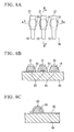
- FIG. 13A is a cross-sectional view taken along the line A-A' in FIG. 1 when the wires 15 are formed so as to cover a portion of the surface of the convex portions 19.
- FIG. 13B is a cross-sectional view taken along the line B-B' in FIG. 1.
- the wires 15 that are provided on the first substrate 10 are formed on each of the convex portions 19, which are formed individually on the first substrate 10, so as to cover the surfaces of the convex portions 19. Namely, in the present embodiment, the wires 15 are also provided with the functions of the conductive layers 21.
- a convex portion 19 and a wire 15 that is formed so as to cover the surface of the convex portion 19 constitute an external connection terminal 27.
- a photolithographic method or in inkjet method can be used for the method of forming the external connection terminals 27.
- a simple explanation is given below only of those points that differ from the first embodiment and second embodiment, and a description of identical portions is omitted.
- a plurality of convex portions 19 are formed on the protruding area 17 of the first substrate 10. These convex portions 19 are placed on the protruding area 17 so as to correspond to positions where electrodes formed on a liquid crystal drive IC 30 are to be packaged.
- the plurality of wires 15 are formed in a predetermined pattern on an area that includes the surfaces of the convex portions 19.
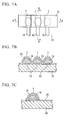
- FIG. 14A is a cross-sectional view taken across a line B-B' in FIG. 1 when the convex portions 19 are formed continuously so as to extend for a plurality of mutually adjacent external connection terminals 27.
- FIG. 14B is a cross-sectional view taken along a line B-B' of the protruding area 17 shown in FIG. 1 in a case in which the height of the convex portions 19 located between adjacent external connection terminals 27 is formed lower than the portions in the external connection terminals 27.
- FIG. 15 of a liquid crystal display apparatus 100 that is provided with the above described liquid crystal panel 25, which is an example of an electro-optical apparatus. Note that because the liquid crystal panel 25 is displayed in detail above, a description thereof is omitted here.
- a liquid crystal drive IC 30 that drives a pixel electrode or the like is chip-on-glass (COG) packaged on the protruding area 17 on the first substrate 10 of the above described liquid crystal panel 25.
- COG chip-on-glass
- connecting terminals of the liquid crystal drive IC 30 and the conductive layers 21 that are formed on the surfaces of the convex portions 19 that are formed from resin on the first substrate 10 are electrically connected via a non-conductive film (NCF, an adhesive agent) or the like.
- NCF non-conductive film
- liquid crystal drive IC 30 and the like can be package on the liquid crystal display apparatus 100, such as a method in which a separate circuit substrate is connected to the liquid crystal panel 25, and the liquid crystal drive IC 30 is chip-on-film (COF) packaged on this circuit substrate.
- COF chip-on-film
- a structure is also employed in which display control signals and the like can be received from an external instrument that is different from this liquid crystal display apparatus 100. It is also preferable that non-electrolytic Ni bumps be formed on the surface of the electrodes of the liquid crystal drive IC 30.
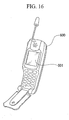
- FIG. 16 is a perspective view showing an example of a mobile telephone.
- the symbol 600 shows a mobile telephone body
- the symbol 601 shows a display unit that is provided with the liquid crystal display apparatus 100 of the above described embodiments.
- the electronic apparatus shown in FIG. 16 is provided with the liquid crystal display apparatus 100 of the above described embodiments, there are few malfunctions in the packaging of the liquid crystal drive IC 30, and a higher level of product quality is achieved.
- the electronic apparatus of the present embodiments is provided with the liquid crystal display device 100, however, the electronic apparatus may also be one that is provided with another electro-optical apparatus such as an organic EL apparatus, a plasma type display apparatus and the like.
- the liquid crystal drive IC 30 is packaged on the first substrate 10 via a conductive paste or the like that does not contain conductive particles in the adhesive agent, however, it is preferable that an adhesive agent that does contain conductive particles be used.
Applications Claiming Priority (2)
| Application Number | Priority Date | Filing Date | Title |
|---|---|---|---|
| JP2004076323 | 2004-03-17 | ||
| JP2004076323A JP3841087B2 (ja) | 2004-03-17 | 2004-03-17 | 電気光学装置用パネル及びその製造方法、電気光学装置、並びに電子機器 |
Publications (2)
| Publication Number | Publication Date |
|---|---|
| EP1577699A2 true EP1577699A2 (fr) | 2005-09-21 |
| EP1577699A3 EP1577699A3 (fr) | 2006-04-26 |
Family
ID=34836544
Family Applications (1)
| Application Number | Title | Priority Date | Filing Date |
|---|---|---|---|
| EP05005366A Withdrawn EP1577699A3 (fr) | 2004-03-17 | 2005-03-11 | Panneau pour appareil éléctro-optique, procédé de fabrication, appareil électro-optique et appareil électronique |
Country Status (6)
| Country | Link |
|---|---|
| US (1) | US7482541B2 (fr) |
| EP (1) | EP1577699A3 (fr) |
| JP (1) | JP3841087B2 (fr) |
| KR (1) | KR100699641B1 (fr) |
| CN (1) | CN100520539C (fr) |
| TW (1) | TWI256128B (fr) |
Cited By (1)
| Publication number | Priority date | Publication date | Assignee | Title |
|---|---|---|---|---|
| CN109448554A (zh) * | 2018-12-03 | 2019-03-08 | 武汉华星光电半导体显示技术有限公司 | 柔性显示面板及其制作方法 |
Families Citing this family (11)
| Publication number | Priority date | Publication date | Assignee | Title |
|---|---|---|---|---|
| JP4292424B2 (ja) * | 2006-11-15 | 2009-07-08 | セイコーエプソン株式会社 | 配線基板およびその製造方法、並びに電子機器 |
| JP4548459B2 (ja) * | 2007-08-21 | 2010-09-22 | セイコーエプソン株式会社 | 電子部品の実装構造体 |
| CN101515074B (zh) * | 2008-02-21 | 2011-08-31 | 北京京东方光电科技有限公司 | 测试液晶面板光学特性的阵列基板电路及其实现方法 |
| KR100953654B1 (ko) | 2008-06-26 | 2010-04-20 | 삼성모바일디스플레이주식회사 | 유기 발광 표시 장치 및 그 제조 방법 |
| US9148957B2 (en) | 2011-03-04 | 2015-09-29 | Sharp Kabushiki Kaisha | Electronic circuit substrate, display device, and wiring substrate |
| KR102058855B1 (ko) * | 2013-12-31 | 2019-12-26 | 엘지디스플레이 주식회사 | 표시장치 |
| CN104035222A (zh) | 2014-06-13 | 2014-09-10 | 京东方科技集团股份有限公司 | 阵列基板、显示面板和显示装置 |
| CN104064539B (zh) | 2014-06-13 | 2017-01-04 | 京东方科技集团股份有限公司 | 显示面板及装置 |
| CN104614911A (zh) * | 2015-03-03 | 2015-05-13 | 京东方科技集团股份有限公司 | 一种基板及其制作方法、显示装置 |
| CN106413270B (zh) * | 2016-11-04 | 2019-04-05 | 大连大学 | 一种氮化铝陶瓷电路板及制备方法 |
| WO2023288030A1 (fr) * | 2021-07-14 | 2023-01-19 | The Trustees Of Dartmouth College | Transistors à oxyde conducteur à ultrahaute mobilité 2d imprimés par métal liquide |
Citations (5)
| Publication number | Priority date | Publication date | Assignee | Title |
|---|---|---|---|---|
| JPH01281433A (ja) | 1988-05-09 | 1989-11-13 | Seiko Epson Corp | 液晶パネル構造 |
| JPH05243231A (ja) | 1992-03-03 | 1993-09-21 | Matsushita Electric Ind Co Ltd | 電子部品実装接続体およびその製造方法 |
| JPH06180460A (ja) | 1992-12-15 | 1994-06-28 | Seiko Epson Corp | 半導体チップ接続用基板構造 |
| EP0827190A2 (fr) | 1994-06-24 | 1998-03-04 | Industrial Technology Research Institute | Structure de plot de contact et méthodes pour sa fabrication |
| JP2004006314A (ja) | 2002-04-18 | 2004-01-08 | Seiko Epson Corp | 電気光学装置及び及びその製造方法、並びに電子機器 |
Family Cites Families (14)
| Publication number | Priority date | Publication date | Assignee | Title |
|---|---|---|---|---|
| US4813129A (en) * | 1987-06-19 | 1989-03-21 | Hewlett-Packard Company | Interconnect structure for PC boards and integrated circuits |
| JPH0621257Y2 (ja) | 1987-07-16 | 1994-06-01 | 三洋電機株式会社 | 固体撮像装置 |
| JP2674033B2 (ja) | 1987-09-18 | 1997-11-05 | セイコーエプソン株式会社 | 液晶装置 |
| JPH03231437A (ja) * | 1990-02-06 | 1991-10-15 | Ricoh Co Ltd | 突起電極形成方法 |
| US5345365A (en) * | 1992-05-05 | 1994-09-06 | Massachusetts Institute Of Technology | Interconnection system for high performance electronic hybrids |
| JPH0697608A (ja) | 1992-09-14 | 1994-04-08 | Nippon Mektron Ltd | 可撓性回路基板の接続部構造及びその形成法 |
| US5393697A (en) * | 1994-05-06 | 1995-02-28 | Industrial Technology Research Institute | Composite bump structure and methods of fabrication |
| JPH088001A (ja) | 1994-06-17 | 1996-01-12 | Yazaki Corp | プリント配線板の回路接続方法 |
| US5657207A (en) * | 1995-03-24 | 1997-08-12 | Packard Hughes Interconnect Company | Alignment means for integrated circuit chips |
| US6396145B1 (en) * | 1998-06-12 | 2002-05-28 | Hitachi, Ltd. | Semiconductor device and method for manufacturing the same technical field |
| JP4035968B2 (ja) | 2000-06-30 | 2008-01-23 | セイコーエプソン株式会社 | 導電膜パターンの形成方法 |
| JP2002164636A (ja) * | 2000-11-27 | 2002-06-07 | Matsushita Electric Works Ltd | 基板に対するスルーホール形成用基準孔の形成方法 |
| JP2004077386A (ja) | 2002-08-21 | 2004-03-11 | Seiko Epson Corp | 半導体実装構造の検査方法、半導体装置の実装構造、電気光学装置及び電子機器 |
| KR20040050245A (ko) | 2002-12-09 | 2004-06-16 | 삼성전자주식회사 | 박막 트랜지스터 기판, 이의 제조방법, 이를 갖는액정표시장치 및 이의 제조방법 |
-
2004
- 2004-03-17 JP JP2004076323A patent/JP3841087B2/ja not_active Expired - Fee Related
-
2005
- 2005-03-04 US US11/073,481 patent/US7482541B2/en not_active Expired - Fee Related
- 2005-03-07 TW TW094106829A patent/TWI256128B/zh not_active IP Right Cessation
- 2005-03-11 EP EP05005366A patent/EP1577699A3/fr not_active Withdrawn
- 2005-03-14 KR KR1020050020894A patent/KR100699641B1/ko not_active IP Right Cessation
- 2005-03-15 CN CNB2005100550445A patent/CN100520539C/zh not_active Expired - Fee Related
Patent Citations (5)
| Publication number | Priority date | Publication date | Assignee | Title |
|---|---|---|---|---|
| JPH01281433A (ja) | 1988-05-09 | 1989-11-13 | Seiko Epson Corp | 液晶パネル構造 |
| JPH05243231A (ja) | 1992-03-03 | 1993-09-21 | Matsushita Electric Ind Co Ltd | 電子部品実装接続体およびその製造方法 |
| JPH06180460A (ja) | 1992-12-15 | 1994-06-28 | Seiko Epson Corp | 半導体チップ接続用基板構造 |
| EP0827190A2 (fr) | 1994-06-24 | 1998-03-04 | Industrial Technology Research Institute | Structure de plot de contact et méthodes pour sa fabrication |
| JP2004006314A (ja) | 2002-04-18 | 2004-01-08 | Seiko Epson Corp | 電気光学装置及び及びその製造方法、並びに電子機器 |
Cited By (1)
| Publication number | Priority date | Publication date | Assignee | Title |
|---|---|---|---|---|
| CN109448554A (zh) * | 2018-12-03 | 2019-03-08 | 武汉华星光电半导体显示技术有限公司 | 柔性显示面板及其制作方法 |
Also Published As
| Publication number | Publication date |
|---|---|
| CN100520539C (zh) | 2009-07-29 |
| US7482541B2 (en) | 2009-01-27 |
| CN1670578A (zh) | 2005-09-21 |
| KR100699641B1 (ko) | 2007-03-23 |
| EP1577699A3 (fr) | 2006-04-26 |
| JP3841087B2 (ja) | 2006-11-01 |
| TWI256128B (en) | 2006-06-01 |
| JP2005266091A (ja) | 2005-09-29 |
| US20050205296A1 (en) | 2005-09-22 |
| KR20060044347A (ko) | 2006-05-16 |
| TW200541048A (en) | 2005-12-16 |
Similar Documents
| Publication | Publication Date | Title |
|---|---|---|
| US7482541B2 (en) | Panel for electro-optical apparatus, method of manufacture thereof, electro-optical apparatus and electronic apparatus | |
| US7547918B2 (en) | Active matrix substrate and electronic device | |
| US7348269B2 (en) | Manufacturing method of semiconductor device, semiconductor device, circuit board, electro-optic device, and electronic apparatus | |
| US8497432B2 (en) | Electronic component mounting structure | |
| US7482271B2 (en) | Manufacturing method for electronic substrate, manufacturing method for electro-optical device, and manufacturing method for electronic device | |
| JP2007286469A (ja) | 膜パターンの形成方法、アクティブマトリクス基板の製造方法、デバイス、電気光学装置、及び電子機器 | |
| JP3906921B2 (ja) | バンプ構造体およびその製造方法 | |
| US8143728B2 (en) | Electronic board and manufacturing method thereof, electro-optical device, and electronic apparatus | |
| US20090208731A1 (en) | Conductive adhesive film, method of producing conductive adhesive film, electronic apparatus including conductive adhesive film, and method of producing electronic apparatus including conductive adhesive film | |
| US5525838A (en) | Semiconductor device with flow preventing member | |
| US20050070046A1 (en) | Method of manufacturing electronic device and method of manufacturing electro-optical device | |
| JP4826852B2 (ja) | 半導体装置、電気光学装置及び電子機器 | |
| JP4862390B2 (ja) | 電子基板の製造方法 | |
| JP2006019630A (ja) | 配線形成方法 | |
| US20050067635A1 (en) | Method of manufacturing electronic component, method of manufacturing electro-optical device, electronic component, and electro-optical device | |
| JP5088309B2 (ja) | 電子基板及び電気光学装置並びに電子機器 | |
| US7645706B2 (en) | Electronic substrate manufacturing method | |
| JP2007149738A (ja) | 電子基板の製造方法、電子基板および電子機器 |
Legal Events
| Date | Code | Title | Description |
|---|---|---|---|
| PUAI | Public reference made under article 153(3) epc to a published international application that has entered the european phase |
Free format text: ORIGINAL CODE: 0009012 |
|
| AK | Designated contracting states |
Kind code of ref document: A2 Designated state(s): AT BE BG CH CY CZ DE DK EE ES FI FR GB GR HU IE IS IT LI LT LU MC NL PL PT RO SE SI SK TR |
|
| AX | Request for extension of the european patent |
Extension state: AL BA HR LV MK YU |
|
| PUAL | Search report despatched |
Free format text: ORIGINAL CODE: 0009013 |
|
| AK | Designated contracting states |
Kind code of ref document: A3 Designated state(s): AT BE BG CH CY CZ DE DK EE ES FI FR GB GR HU IE IS IT LI LT LU MC NL PL PT RO SE SI SK TR |
|
| AX | Request for extension of the european patent |
Extension state: AL BA HR LV MK YU |
|
| 17P | Request for examination filed |
Effective date: 20060613 |
|
| AKX | Designation fees paid |
Designated state(s): DE FR GB |
|
| 17Q | First examination report despatched |
Effective date: 20090225 |
|
| STAA | Information on the status of an ep patent application or granted ep patent |
Free format text: STATUS: THE APPLICATION IS DEEMED TO BE WITHDRAWN |
|
| 18D | Application deemed to be withdrawn |
Effective date: 20101001 |