EP1575162B1 - Tonfrequenzverstärker - Google Patents
Tonfrequenzverstärker Download PDFInfo
- Publication number
- EP1575162B1 EP1575162B1 EP03778853.6A EP03778853A EP1575162B1 EP 1575162 B1 EP1575162 B1 EP 1575162B1 EP 03778853 A EP03778853 A EP 03778853A EP 1575162 B1 EP1575162 B1 EP 1575162B1
- Authority
- EP
- European Patent Office
- Prior art keywords
- signal
- circuit
- clock
- digital audio
- supplied
- Prior art date
- Legal status (The legal status is an assumption and is not a legal conclusion. Google has not performed a legal analysis and makes no representation as to the accuracy of the status listed.)
- Expired - Lifetime
Links
Images

Classifications
-
- H—ELECTRICITY
- H03—ELECTRONIC CIRCUITRY
- H03F—AMPLIFIERS
- H03F3/00—Amplifiers with only discharge tubes or only semiconductor devices as amplifying elements
- H03F3/20—Power amplifiers, e.g. Class B amplifiers, Class C amplifiers
- H03F3/21—Power amplifiers, e.g. Class B amplifiers, Class C amplifiers with semiconductor devices only
- H03F3/217—Class D power amplifiers; Switching amplifiers
- H03F3/2175—Class D power amplifiers; Switching amplifiers using analogue-digital or digital-analogue conversion
-
- H—ELECTRICITY
- H03—ELECTRONIC CIRCUITRY
- H03F—AMPLIFIERS
- H03F1/00—Details of amplifiers with only discharge tubes, only semiconductor devices or only unspecified devices as amplifying elements
- H03F1/26—Modifications of amplifiers to reduce influence of noise generated by amplifying elements
-
- H—ELECTRICITY
- H03—ELECTRONIC CIRCUITRY
- H03F—AMPLIFIERS
- H03F3/00—Amplifiers with only discharge tubes or only semiconductor devices as amplifying elements
- H03F3/181—Low-frequency amplifiers, e.g. audio preamplifiers
-
- H—ELECTRICITY
- H03—ELECTRONIC CIRCUITRY
- H03G—CONTROL OF AMPLIFICATION
- H03G3/00—Gain control in amplifiers or frequency changers
- H03G3/20—Automatic control
- H03G3/30—Automatic control in amplifiers having semiconductor devices
- H03G3/34—Muting amplifier when no signal is present
-
- H—ELECTRICITY
- H03—ELECTRONIC CIRCUITRY
- H03M—CODING; DECODING; CODE CONVERSION IN GENERAL
- H03M3/00—Conversion of analogue values to or from differential modulation
- H03M3/30—Delta-sigma modulation
- H03M3/322—Continuously compensating for, or preventing, undesired influence of physical parameters
- H03M3/324—Continuously compensating for, or preventing, undesired influence of physical parameters characterised by means or methods for compensating or preventing more than one type of error at a time, e.g. by synchronisation or using a ratiometric arrangement
- H03M3/346—Continuously compensating for, or preventing, undesired influence of physical parameters characterised by means or methods for compensating or preventing more than one type of error at a time, e.g. by synchronisation or using a ratiometric arrangement by suppressing active signals at predetermined times, e.g. muting, using non-overlapping clock phases
-
- H—ELECTRICITY
- H03—ELECTRONIC CIRCUITRY
- H03F—AMPLIFIERS
- H03F2200/00—Indexing scheme relating to amplifiers
- H03F2200/331—Sigma delta modulation being used in an amplifying circuit
-
- H—ELECTRICITY
- H03—ELECTRONIC CIRCUITRY
- H03M—CODING; DECODING; CODE CONVERSION IN GENERAL
- H03M3/00—Conversion of analogue values to or from differential modulation
- H03M3/30—Delta-sigma modulation
- H03M3/322—Continuously compensating for, or preventing, undesired influence of physical parameters
- H03M3/324—Continuously compensating for, or preventing, undesired influence of physical parameters characterised by means or methods for compensating or preventing more than one type of error at a time, e.g. by synchronisation or using a ratiometric arrangement
- H03M3/326—Continuously compensating for, or preventing, undesired influence of physical parameters characterised by means or methods for compensating or preventing more than one type of error at a time, e.g. by synchronisation or using a ratiometric arrangement by averaging out the errors
- H03M3/328—Continuously compensating for, or preventing, undesired influence of physical parameters characterised by means or methods for compensating or preventing more than one type of error at a time, e.g. by synchronisation or using a ratiometric arrangement by averaging out the errors using dither
-
- H—ELECTRICITY
- H03—ELECTRONIC CIRCUITRY
- H03M—CODING; DECODING; CODE CONVERSION IN GENERAL
- H03M3/00—Conversion of analogue values to or from differential modulation
- H03M3/30—Delta-sigma modulation
- H03M3/50—Digital/analogue converters using delta-sigma modulation as an intermediate step
- H03M3/502—Details of the final digital/analogue conversion following the digital delta-sigma modulation
- H03M3/506—Details of the final digital/analogue conversion following the digital delta-sigma modulation the final digital/analogue converter being constituted by a pulse width modulator
Definitions
- This invention relates to an audio amplifier.
- a power amplifier of a final stage is configured with a so-called D-class amplifier, a whole is able to be digitized, and is able to be configured as a digital audio amplifier.
- Fig. 3 shows one example of such digital audio amplifier.
- a digital audio signal S11 is supplied to an over-sampling circuit 12 from an input terminal 11, a sampling frequency thereof is over-sampled to be a digital signal S12 of 8 times, this digital signal S12 is supplied to a ⁇ modulation circuit 14 through a variable attenuator circuit 13 for volume control, and is re-quantized to be bit-reduced digital signal S14.
- this digital signal S14 is supplied to a PWM modulation circuit 15, and converted to a PWM signal S15, then this PWM signal S15 is supplied to a power amplifier 16 operating in D-class.
- This power amplifier 16 is configured with a switching circuit for power amplifying by switching a power source voltage in accordance with the PWM signal S15, and a low pass filter for outputting a D/A converted and power amplified analog audio signal by smoothing the switching output. Further, by the power amplifier 16, the power amplified audio signal is supplied to a speaker 30 through an output terminal 17.
- a volume control signal SVOL is formed, and this signal SVOL is supplied to the variable attenuator circuit 13 as a control signal. Accordingly, when a switch for the volume control is operated, an attenuation level of the variable attenuator circuit 13 is changed, and a volume of a reproduced sound outputted from the speaker 30 is changed.
- the ⁇ modulation circuit 14 includes a feedback loop for a quantizing error, so that even if a content of the digital signal S12 supplied from the variable attenuator circuit 13 to the ⁇ modulation circuit 14 is zero, a digital signal S14 having something value is accordingly outputted from the ⁇ modulation circuit 14, and the digital signal S14 is accordingly outputted from the speaker 30 as a noise sound having a specified frequency.
- a dither signal SDI of a minute level is formed, this dither signal SDI is supplied to the ⁇ modulation circuit 14, and is superimposed on the digital signal S12 upon re-quantization. Accordingly, even in a case where the content of the digital signal S12 outputted from the variable attenuator circuit 13 is zero, an actual content of the ⁇ modulation circuit 15 does not become zero, so that it is suppressed to output the noise sound.
- the digital signal S11 supplied to the input terminal 11 is supplied to an asynchronous detection circuit 19, and a disturbance of synchronization of the digital signal S11 is detected. Further, this detection signal SDET is supplied to the circuits 12 to 14 as a muting signal, and when the synchronization of the digital signal S11 is disturbed, the contents of the signals S12 and S14 are set to be zero, and as the result, the reproduced sound outputted from the speaker 30 is muted.
- the above is one example of an audio amplifier where the power amplifier 17 in the final stage is configured with a D-class amplifier (See Japanese Laid-open Patent Application OP2002-158543 , for example).
- the dither signal SDI has a minute level
- the presence/absence of the dither signal SDI is able to be recognized as a difference in a noise level. Therefore, when the muting is set to be on, the noise level changes because the dither signal SDI is muted, but in a case where the content of the input digital signal S11 is zero (or a minute level), the change in the noise level is recognized, and this causes uncomfortable feeling.
- the dither signal is continuously supplied to the ⁇ modulation circuit even during muting, and the digital audio signal including the dither signal is supplied to the D-class power amplifier after converting into the PWM signal.
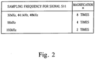
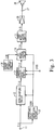
- Fig. 1 shows one example of a digital audio amplifier 10 according to the present invention, and a digital audio signal S11 is supplied to an over-sampling circuit 12 through an input terminal 11. Further, the digital signal S11 from the input terminal 11 is supplied to a PLL 21, a clock SPLL synchronized with the digital signal S11 and having a frequency of n times of its sampling frequency is formed, and thus generated clock SPLL is supplied to the over-sampling circuit 12 as a clock for over-sampling.
- the magnification n of the over-sampling is set to be a value as shown in Fig. 2 corresponding to the sampling frequency of the digital signal S11.
- the digital signal S11 supplied thereto is over-sampled to a digital signal S12 synchronized with the signal S11, and having a frequency of n times the sampling frequency.
- this digital signal S12 is supplied to the sampling rate converter circuit 23 as a conversion input. Further, the clock SPLL from the PLL 21 is supplied to the sampling rate converter circuit 23 as a clock for conversion input side.
- the sampling rate converted digital signal S23 is supplied to the variable attenuator circuit 13 for the volume control, the level thereof is controlled by the control signal SVOL from the system controller (not illustrated), the level controlled digital signal S12 is supplied to the ⁇ modulation circuit 14, and is re-quantized into a bit-reduced digital signal S14.
- the dither signal forming circuit 18 the dither signal SDI of a minute level is formed at this time, and this dither signal SDI is superimposed on the digital signal S23 to be supplied to the ⁇ modulation circuit 14.
- the digital signal S14 re-quantized by the ⁇ modulation circuit 14 is supplied to the PWM modulation circuit 15, and is converted into a PWM signal S15.
- This PWM signal S15 is then supplied to the power amplifier 16 operating in D class, and power amplified, and after that, thus amplified output is supplied to the speaker 30 through the output terminal 17.
- the clock SGEN from the forming circuit 22 is supplied to the circuits 13 to 15, and 18 as their clocks. Accordingly, the output side of the sampling rate converter circuit 23 and the circuits 13 to 15, and 18 are to be operated in synchronism with the clock SGEN.
- the digital signal S11 supplied to the input terminal 11 is supplied to the asynchronous detection circuit 19, also the clock having a frequency equal to the sampling frequency of the input digital signal S11 and synchronized thereto is derived from the PLL 21, this clock is supplied to the asynchronous detection circuit 19, and a disturbance of the synchronization of the digital signal S11 supplied to the input terminal 11 is detected.
- the detection signal SDET is supplied to the over-sampling circuit 12, an input side of the sampling rate converter circuit 23, and the variable attenuator circuit 13 as a muting signal, and when a synchronization of the digital signal S11 is disturbed, the content of the signal S12 is set to be zero, and also the operation of the input side in the sampling rate converter circuit 23 is stopped.
- the digital audio signal S11 supplied to the input terminal 11 in spite of its sampling frequency, the sampling frequency is converted its sampling rate into the digital signal having a sampling frequency of 384 kHz by the sampling rate converter circuit 23, and after that, it is power amplified after converted into the PWM signal S15, then supplied to the speaker 30.
- the synchronization of the digital signal S11 is temporary disturbed, and this disturbance of synchronization is detected by the asynchronous detection circuit 19, and by the detection signal SDET, the over-sampling circuit 12 and the input side of the sampling rate converter circuit 23 are stopped. Accordingly, the digital signal S12 is to be shut out during an interval of the detection signal SDET.
- the digital signal S23 is continuously outputted from the sampling rate converter circuit 23, because the output side thereof is supplied with the clock SGEN, and the operation is continuous.
- the muting is performed, however, even during the muting interval, the dither signal SDI is supplied to the ⁇ modulation circuit 14, and accordingly, even if the content of the digital signal S23 supplied thereto is zero, it never happens to output from the ⁇ modulation circuit 14 the signal components which become a noise sound of a particular frequency.
- the noise levels become equal between when the muting is off and when the muting is on. Accordingly, in a case when the content of the input digital signal S11 is zero (or, a minute level), if a muting is activated, there is no fear of being recognized the change in the noise level and uncomfortable feeling.
- the dither signal SDI is always continuing, so that there is no fear of generating noise signals, and also there is no fear of outputting a noise sound from the speaker 30.
- the present invention even if a muting is on when the content of the input digital audio signal is zero, or a minute level, there is no fear of uncomfortable feeling due to the recognition of the change in the noise level. Further, when the muting is made on from the muting off state, or when the muting is released from the muting on state, there is no fear of generating noise signals, and also there is no fear of outputting a noise sound from the speaker.
Landscapes
- Engineering & Computer Science (AREA)
- Power Engineering (AREA)
- Multimedia (AREA)
- Theoretical Computer Science (AREA)
- Amplifiers (AREA)
Claims (2)
- Audioverstärker, umfassend:eine ΔΣ-Modulationsschaltung (14) zum erneuten Quantisieren eines digitalen Audiosignals in ein bitreduziertes digitales Audiosignal;eine PWM-Modulationsschaltung (15) zum Umwandeln des bitreduzierten digitalen Audiosignals in ein PWM-Signal; undeinen D-Klasse-Leistungsverstärker (16), der mit dem von der PWM-Modulationsschaltung (15) ausgegebenen PWM-Signal versorgt wird,eine PLL-Schaltung (21), die angepasst ist, um das digitale Audiosignal (S11) zu empfangen und einen ersten Takt (SPLL) zu bilden, der mit dem digitalen Audiosignal (S11) synchronisiert ist;eine Taktgeberschaltung (22) zum Bereitstellen eines zweiten Takts (SGEN) mit einer stabilen und vorbestimmten Frequenz;eine asynchrone Erkennungsschaltung (19), die angepasst ist, einen asynchronen Zustand des digitalen Audiosignals (S11) zu erkennen, zur Bildung eines Stummschaltungssignals (SDET) bei Erkennung;eine Abtastraten-Wandlerschaltung (23), die angepasst ist, mit dem Stummschaltungssignal (SDET) auf ihrer Eingangsseite, dem ersten Takt (SPLL) als Takt für die Umwandlungs-Eingangsseite, und dem zweiten Takt (SGEN) als Takt für die Umwandlungs-Ausgangsseite versorgt zu werden, und angepasst ist, eine Abtastrate des digitalen Audiosignals (S11) mit dem ersten Takt (SPLL) und mit dem zweiten Takt (SGEN) in ein umgewandeltes digitales Audiosignal (S23) umzuwandeln, das mit dem zweiten Takt (SGEN) synchronisiert ist, und das umgewandelte digitale Audiosignal (S23) an die ΔΣ-Modulationsschaltung (14) auszugeben, selbst wenn eine Eingangsseite der Abtastraten-Wandlerschaltung (23) gestoppt wird, wenn das Stummschaltsignal empfangen wird; undeine Dithersignal-Erzeugungsschaltung (18), die angepasst ist, um ein Dithersignal an die ΔΣ-Modulationsschaltung (14) zu liefern, zur Überlagerung des Dithersignals über das umgewandelte digitale Audiosignal (S23), selbst wenn das Stummschaltungssignal (SDET) durch die asynchrone Erkennungsschaltung (19) vorgesehen ist.
- Audioverstärker nach Anspruch 1, wobei die asynchrone Erkennungsschaltung (19) angepasst ist, von der PLL-Schaltung (21) einen Takt zu empfangen, der mit dem digitalen Audiosignal (S11) synchronisiert ist.
Applications Claiming Priority (3)
| Application Number | Priority Date | Filing Date | Title |
|---|---|---|---|
| JP2002369703 | 2002-12-20 | ||
| JP2002369703A JP4078543B2 (ja) | 2002-12-20 | 2002-12-20 | オーディオアンプ |
| PCT/JP2003/015916 WO2004057757A1 (ja) | 2002-12-20 | 2003-12-12 | オーディオアンプ |
Publications (3)
| Publication Number | Publication Date |
|---|---|
| EP1575162A1 EP1575162A1 (de) | 2005-09-14 |
| EP1575162A4 EP1575162A4 (de) | 2006-09-06 |
| EP1575162B1 true EP1575162B1 (de) | 2018-07-11 |
Family
ID=32677148
Family Applications (1)
| Application Number | Title | Priority Date | Filing Date |
|---|---|---|---|
| EP03778853.6A Expired - Lifetime EP1575162B1 (de) | 2002-12-20 | 2003-12-12 | Tonfrequenzverstärker |
Country Status (6)
| Country | Link |
|---|---|
| US (1) | US7209002B2 (de) |
| EP (1) | EP1575162B1 (de) |
| JP (1) | JP4078543B2 (de) |
| KR (1) | KR101015724B1 (de) |
| CN (1) | CN100459423C (de) |
| WO (1) | WO2004057757A1 (de) |
Families Citing this family (20)
| Publication number | Priority date | Publication date | Assignee | Title |
|---|---|---|---|---|
| JP4120829B2 (ja) * | 2004-07-30 | 2008-07-16 | ソニー株式会社 | パワーアンプ装置およびdc成分除去方法 |
| JP2006054545A (ja) * | 2004-08-10 | 2006-02-23 | Matsushita Electric Ind Co Ltd | ディジタルゲイン制御装置とそれを用いたオーディオ信号電力増幅装置、並びにそれらの方法 |
| CN100417017C (zh) * | 2005-02-17 | 2008-09-03 | 普诚科技股份有限公司 | D类音频放大器的异步式桥接负载 |
| JP4704887B2 (ja) * | 2005-10-28 | 2011-06-22 | Okiセミコンダクタ株式会社 | 増幅回路 |
| JP4513021B2 (ja) * | 2005-12-28 | 2010-07-28 | ソニー株式会社 | ディジタルアンプ装置及びディジタルアンプ装置のミュート方法 |
| JP4513022B2 (ja) * | 2005-12-28 | 2010-07-28 | ソニー株式会社 | ディジタルアンプ装置及びディジタルアンプ装置のリセット方法 |
| JP4311437B2 (ja) * | 2006-11-15 | 2009-08-12 | ヤマハ株式会社 | D級増幅装置 |
| TWI329983B (en) * | 2006-11-27 | 2010-09-01 | Realtek Semiconductor Corp | Methods for controlling power stage of power amplifier and related apparatuses |
| JP2008187375A (ja) * | 2007-01-29 | 2008-08-14 | Rohm Co Ltd | アナログデジタル変換器およびそれを用いた電子機器 |
| US8090212B1 (en) | 2007-12-21 | 2012-01-03 | Zoran Corporation | Method, apparatus, and system for reducing blurring of an image using multiple filtered images |
| CN101527547B (zh) * | 2008-03-07 | 2015-03-04 | 瑞昱半导体股份有限公司 | 控制功率放大器的功率输出级的方法及相关装置 |
| JP2010045726A (ja) * | 2008-08-18 | 2010-02-25 | Sharp Corp | 信号増幅装置及び信号処理方法 |
| KR101069234B1 (ko) | 2008-10-14 | 2011-10-04 | (주)제이디에이테크놀로지 | 무 필터 d 급 오디오 증폭기 |
| KR101573343B1 (ko) | 2009-06-16 | 2015-12-02 | 삼성전자주식회사 | 플립플롭 회로 및 이를 구비하는 컴퓨터 시스템 |
| US8306106B2 (en) | 2010-04-27 | 2012-11-06 | Equiphon, Inc. | Multi-edge pulse width modulator with non-stationary residue assignment |
| JP5017428B2 (ja) * | 2010-06-30 | 2012-09-05 | 株式会社東芝 | 変調信号処理装置及び変調信号処理方法 |
| CN104168524A (zh) * | 2013-05-17 | 2014-11-26 | 无锡华润矽科微电子有限公司 | 数字功放设备的控制电路及其控制方法 |
| CN103763591A (zh) * | 2014-01-10 | 2014-04-30 | 广东雷洋电子科技有限公司 | 一种大功率视频播放器 |
| CN104104342B (zh) * | 2014-06-27 | 2017-05-24 | 同济大学 | 一种二次量化器、采用其的d类放大器以及音频设备 |
| CN109756193B (zh) * | 2017-11-01 | 2023-04-28 | 华润微集成电路(无锡)有限公司 | 使用扩谱调制进行pwm波调制的d类数字音频功放系统 |
Family Cites Families (12)
| Publication number | Priority date | Publication date | Assignee | Title |
|---|---|---|---|---|
| JPH07120950B2 (ja) | 1990-09-05 | 1995-12-20 | ヤマハ株式会社 | Da変換装置 |
| US5672998A (en) * | 1995-08-09 | 1997-09-30 | Harris Corporation | Class D amplifier and method |
| JP3304750B2 (ja) * | 1996-03-27 | 2002-07-22 | 松下電器産業株式会社 | ロスレス符号装置とロスレス記録媒体とロスレス復号装置とロスレス符号復号装置 |
| US5777512A (en) * | 1996-06-20 | 1998-07-07 | Tripath Technology, Inc. | Method and apparatus for oversampled, noise-shaping, mixed-signal processing |
| US6014055A (en) * | 1998-02-06 | 2000-01-11 | Intersil Corporation | Class D amplifier with reduced clock requirement and related methods |
| US6373336B1 (en) * | 1998-07-24 | 2002-04-16 | Texas Instruments, Copenhagen Aps | Method of attenuating zero crossing distortion and noise in an amplifier, an amplifier and uses of the method and the amplifier |
| WO2000070752A1 (fr) * | 1999-05-18 | 2000-11-23 | Lucent Technologies Inc. | Amplificateur numerique |
| JP3681105B2 (ja) * | 2000-02-24 | 2005-08-10 | アルパイン株式会社 | データ処理方式 |
| JP2002158550A (ja) | 2000-11-17 | 2002-05-31 | Sony Corp | デジタルパワーアンプ |
| JP2002158549A (ja) * | 2000-11-17 | 2002-05-31 | Sony Corp | デジタルパワーアンプ装置 |
| JP2002158543A (ja) | 2000-11-17 | 2002-05-31 | Sony Corp | デジタルパワーアンプ |
| EP1469594A1 (de) * | 2003-04-17 | 2004-10-20 | Dialog Semiconductor GmbH | Multipegel Klasse-D Verstärker mit zwei Ausgangsniveaus |
-
2002
- 2002-12-20 JP JP2002369703A patent/JP4078543B2/ja not_active Expired - Fee Related
-
2003
- 2003-12-12 KR KR1020057011200A patent/KR101015724B1/ko not_active Expired - Fee Related
- 2003-12-12 US US10/536,999 patent/US7209002B2/en not_active Expired - Lifetime
- 2003-12-12 CN CNB2003801057153A patent/CN100459423C/zh not_active Expired - Fee Related
- 2003-12-12 EP EP03778853.6A patent/EP1575162B1/de not_active Expired - Lifetime
- 2003-12-12 WO PCT/JP2003/015916 patent/WO2004057757A1/ja not_active Ceased
Non-Patent Citations (1)
| Title |
|---|
| None * |
Also Published As
| Publication number | Publication date |
|---|---|
| US20050285670A1 (en) | 2005-12-29 |
| KR20050089158A (ko) | 2005-09-07 |
| CN100459423C (zh) | 2009-02-04 |
| EP1575162A4 (de) | 2006-09-06 |
| KR101015724B1 (ko) | 2011-02-22 |
| JP4078543B2 (ja) | 2008-04-23 |
| JP2004201185A (ja) | 2004-07-15 |
| US7209002B2 (en) | 2007-04-24 |
| CN1723616A (zh) | 2006-01-18 |
| WO2004057757A1 (ja) | 2004-07-08 |
| EP1575162A1 (de) | 2005-09-14 |
Similar Documents
| Publication | Publication Date | Title |
|---|---|---|
| EP1575162B1 (de) | Tonfrequenzverstärker | |
| JP3274469B2 (ja) | 補聴器 | |
| EP1435695B1 (de) | Delta-sigma-modulationsvorrichtung und signalverstärkungsvorrichtung | |
| US5672998A (en) | Class D amplifier and method | |
| JP3369503B2 (ja) | ディジタルスイッチングアンプ | |
| WO2000051122A8 (en) | Clock generation circuit | |
| US7113030B2 (en) | Class-D power amplifier capable of eliminating excessive response phenomenon when returning to a steady state from an abnormal state and an amplification method thereof | |
| CN100555845C (zh) | 用于校正放大设备中的信号失真的方法和设备 | |
| US6297693B1 (en) | Techniques for synchronizing a self oscillating variable frequency modulator to an external clock | |
| WO1999056427A3 (en) | Sample rate converter using polynomial interpolation | |
| US20100277356A1 (en) | Oscillation frequency control circuit, dc-dc converter including the oscillation frequency control circuit, and semiconductor device | |
| JP5194663B2 (ja) | 半導体装置 | |
| JPH07254823A (ja) | デルタシグマ変調増幅器 | |
| AU7566901A (en) | Linear dead-band-free digital phase detection | |
| JP2950493B2 (ja) | 映像処理システムのバースト信号発生回路 | |
| US7340070B2 (en) | Voice-data processing circuit and voice-data processing method | |
| JP4564912B2 (ja) | 信号再生装置 | |
| JP2697650B2 (ja) | フィードフォワード増幅器 | |
| WO2003052941A3 (de) | Breitbandiger sigma-delta modulator | |
| US9559678B2 (en) | Generation of analog signal based on one-bit signal | |
| WO2005086350A3 (de) | Frequenzteilerschaltung mit steuerbarem frequenzteilerverhältnis und verfahren zur frequenzteilung in einer frequenzteilerschaltung | |
| JP2009044321A (ja) | 音声信号処理装置 | |
| JPH0496428A (ja) | 無線装置 | |
| KR100362879B1 (ko) | 고속위상 고착을 위한 위상동기루프 제어회로 | |
| KR100188983B1 (ko) | 소음레벨에 따라 자동으로 음량이 조절되는 스피커음량조절회로 |
Legal Events
| Date | Code | Title | Description |
|---|---|---|---|
| PUAI | Public reference made under article 153(3) epc to a published international application that has entered the european phase |
Free format text: ORIGINAL CODE: 0009012 |
|
| 17P | Request for examination filed |
Effective date: 20050610 |
|
| AK | Designated contracting states |
Kind code of ref document: A1 Designated state(s): AT BE BG CH CY CZ DE DK EE ES FI FR GB GR HU IE IT LI LU MC NL PT RO SE SI SK TR |
|
| RBV | Designated contracting states (corrected) |
Designated state(s): DE FR GB |
|
| A4 | Supplementary search report drawn up and despatched |
Effective date: 20060803 |
|
| RIC1 | Information provided on ipc code assigned before grant |
Ipc: H03F 3/217 20060101AFI20040715BHEP Ipc: H03G 3/34 20060101ALI20060728BHEP Ipc: H03F 3/181 20060101ALI20060728BHEP Ipc: H03M 3/02 20060101ALI20060728BHEP |
|
| 17Q | First examination report despatched |
Effective date: 20070921 |
|
| GRAP | Despatch of communication of intention to grant a patent |
Free format text: ORIGINAL CODE: EPIDOSNIGR1 |
|
| RIC1 | Information provided on ipc code assigned before grant |
Ipc: H03G 3/34 20060101ALI20180119BHEP Ipc: H03F 3/181 20060101ALI20180119BHEP Ipc: H03F 3/217 20060101AFI20180119BHEP Ipc: H03M 3/00 20060101ALI20180119BHEP |
|
| INTG | Intention to grant announced |
Effective date: 20180206 |
|
| GRAS | Grant fee paid |
Free format text: ORIGINAL CODE: EPIDOSNIGR3 |
|
| GRAA | (expected) grant |
Free format text: ORIGINAL CODE: 0009210 |
|
| AK | Designated contracting states |
Kind code of ref document: B1 Designated state(s): DE FR GB |
|
| REG | Reference to a national code |
Ref country code: GB Ref legal event code: FG4D |
|
| REG | Reference to a national code |
Ref country code: DE Ref legal event code: R096 Ref document number: 60351318 Country of ref document: DE |
|
| RIC2 | Information provided on ipc code assigned after grant |
Ipc: H03F 3/217 20060101AFI20180119BHEP Ipc: H03G 3/34 20060101ALI20180119BHEP Ipc: H03F 3/181 20060101ALI20180119BHEP Ipc: H03M 3/00 20060101ALI20180119BHEP |
|
| REG | Reference to a national code |
Ref country code: DE Ref legal event code: R097 Ref document number: 60351318 Country of ref document: DE |
|
| PLBE | No opposition filed within time limit |
Free format text: ORIGINAL CODE: 0009261 |
|
| STAA | Information on the status of an ep patent application or granted ep patent |
Free format text: STATUS: NO OPPOSITION FILED WITHIN TIME LIMIT |
|
| 26N | No opposition filed |
Effective date: 20190412 |
|
| PGFP | Annual fee paid to national office [announced via postgrant information from national office to epo] |
Ref country code: FR Payment date: 20191219 Year of fee payment: 17 |
|
| PGFP | Annual fee paid to national office [announced via postgrant information from national office to epo] |
Ref country code: GB Payment date: 20191220 Year of fee payment: 17 |
|
| PGFP | Annual fee paid to national office [announced via postgrant information from national office to epo] |
Ref country code: DE Payment date: 20201211 Year of fee payment: 18 |
|
| GBPC | Gb: european patent ceased through non-payment of renewal fee |
Effective date: 20201212 |
|
| PG25 | Lapsed in a contracting state [announced via postgrant information from national office to epo] |
Ref country code: FR Free format text: LAPSE BECAUSE OF NON-PAYMENT OF DUE FEES Effective date: 20201231 |
|
| PG25 | Lapsed in a contracting state [announced via postgrant information from national office to epo] |
Ref country code: GB Free format text: LAPSE BECAUSE OF NON-PAYMENT OF DUE FEES Effective date: 20201212 |
|
| REG | Reference to a national code |
Ref country code: DE Ref legal event code: R119 Ref document number: 60351318 Country of ref document: DE |
|
| PG25 | Lapsed in a contracting state [announced via postgrant information from national office to epo] |
Ref country code: DE Free format text: LAPSE BECAUSE OF NON-PAYMENT OF DUE FEES Effective date: 20220701 |