EP1562169A2 - Doppel-Flachbildanzeige - Google Patents
Doppel-Flachbildanzeige Download PDFInfo
- Publication number
- EP1562169A2 EP1562169A2 EP04090358A EP04090358A EP1562169A2 EP 1562169 A2 EP1562169 A2 EP 1562169A2 EP 04090358 A EP04090358 A EP 04090358A EP 04090358 A EP04090358 A EP 04090358A EP 1562169 A2 EP1562169 A2 EP 1562169A2
- Authority
- EP
- European Patent Office
- Prior art keywords
- display device
- flat panel
- panel display
- lines
- data
- Prior art date
- Legal status (The legal status is an assumption and is not a legal conclusion. Google has not performed a legal analysis and makes no representation as to the accuracy of the status listed.)
- Ceased
Links
Images

Classifications
-
- G—PHYSICS
- G09—EDUCATION; CRYPTOGRAPHY; DISPLAY; ADVERTISING; SEALS
- G09G—ARRANGEMENTS OR CIRCUITS FOR CONTROL OF INDICATING DEVICES USING STATIC MEANS TO PRESENT VARIABLE INFORMATION
- G09G3/00—Control arrangements or circuits, of interest only in connection with visual indicators other than cathode-ray tubes
- G09G3/20—Control arrangements or circuits, of interest only in connection with visual indicators other than cathode-ray tubes for presentation of an assembly of a number of characters, e.g. a page, by composing the assembly by combination of individual elements arranged in a matrix no fixed position being assigned to or needed to be assigned to the individual characters or partial characters
- G09G3/34—Control arrangements or circuits, of interest only in connection with visual indicators other than cathode-ray tubes for presentation of an assembly of a number of characters, e.g. a page, by composing the assembly by combination of individual elements arranged in a matrix no fixed position being assigned to or needed to be assigned to the individual characters or partial characters by control of light from an independent source
- G09G3/36—Control arrangements or circuits, of interest only in connection with visual indicators other than cathode-ray tubes for presentation of an assembly of a number of characters, e.g. a page, by composing the assembly by combination of individual elements arranged in a matrix no fixed position being assigned to or needed to be assigned to the individual characters or partial characters by control of light from an independent source using liquid crystals
- G09G3/3611—Control of matrices with row and column drivers
-
- H—ELECTRICITY
- H01—ELECTRIC ELEMENTS
- H01R—ELECTRICALLY-CONDUCTIVE CONNECTIONS; STRUCTURAL ASSOCIATIONS OF A PLURALITY OF MUTUALLY-INSULATED ELECTRICAL CONNECTING ELEMENTS; COUPLING DEVICES; CURRENT COLLECTORS
- H01R31/00—Coupling parts supported only by co-operation with counterpart
- H01R31/06—Intermediate parts for linking two coupling parts, e.g. adapter
-
- G—PHYSICS
- G09—EDUCATION; CRYPTOGRAPHY; DISPLAY; ADVERTISING; SEALS
- G09G—ARRANGEMENTS OR CIRCUITS FOR CONTROL OF INDICATING DEVICES USING STATIC MEANS TO PRESENT VARIABLE INFORMATION
- G09G3/00—Control arrangements or circuits, of interest only in connection with visual indicators other than cathode-ray tubes
- G09G3/20—Control arrangements or circuits, of interest only in connection with visual indicators other than cathode-ray tubes for presentation of an assembly of a number of characters, e.g. a page, by composing the assembly by combination of individual elements arranged in a matrix no fixed position being assigned to or needed to be assigned to the individual characters or partial characters
- G09G3/34—Control arrangements or circuits, of interest only in connection with visual indicators other than cathode-ray tubes for presentation of an assembly of a number of characters, e.g. a page, by composing the assembly by combination of individual elements arranged in a matrix no fixed position being assigned to or needed to be assigned to the individual characters or partial characters by control of light from an independent source
- G09G3/36—Control arrangements or circuits, of interest only in connection with visual indicators other than cathode-ray tubes for presentation of an assembly of a number of characters, e.g. a page, by composing the assembly by combination of individual elements arranged in a matrix no fixed position being assigned to or needed to be assigned to the individual characters or partial characters by control of light from an independent source using liquid crystals
- G09G3/3611—Control of matrices with row and column drivers
- G09G3/3674—Details of drivers for scan electrodes
- G09G3/3677—Details of drivers for scan electrodes suitable for active matrices only
-
- G—PHYSICS
- G02—OPTICS
- G02F—OPTICAL DEVICES OR ARRANGEMENTS FOR THE CONTROL OF LIGHT BY MODIFICATION OF THE OPTICAL PROPERTIES OF THE MEDIA OF THE ELEMENTS INVOLVED THEREIN; NON-LINEAR OPTICS; FREQUENCY-CHANGING OF LIGHT; OPTICAL LOGIC ELEMENTS; OPTICAL ANALOGUE/DIGITAL CONVERTERS
- G02F1/00—Devices or arrangements for the control of the intensity, colour, phase, polarisation or direction of light arriving from an independent light source, e.g. switching, gating or modulating; Non-linear optics
- G02F1/01—Devices or arrangements for the control of the intensity, colour, phase, polarisation or direction of light arriving from an independent light source, e.g. switching, gating or modulating; Non-linear optics for the control of the intensity, phase, polarisation or colour
- G02F1/13—Devices or arrangements for the control of the intensity, colour, phase, polarisation or direction of light arriving from an independent light source, e.g. switching, gating or modulating; Non-linear optics for the control of the intensity, phase, polarisation or colour based on liquid crystals, e.g. single liquid crystal display cells
- G02F1/133—Constructional arrangements; Operation of liquid crystal cells; Circuit arrangements
- G02F1/1333—Constructional arrangements; Manufacturing methods
- G02F1/133342—Constructional arrangements; Manufacturing methods for double-sided displays
-
- G—PHYSICS
- G06—COMPUTING OR CALCULATING; COUNTING
- G06F—ELECTRIC DIGITAL DATA PROCESSING
- G06F2213/00—Indexing scheme relating to interconnection of, or transfer of information or other signals between, memories, input/output devices or central processing units
- G06F2213/0042—Universal serial bus [USB]
-
- G—PHYSICS
- G06—COMPUTING OR CALCULATING; COUNTING
- G06F—ELECTRIC DIGITAL DATA PROCESSING
- G06F3/00—Input arrangements for transferring data to be processed into a form capable of being handled by the computer; Output arrangements for transferring data from processing unit to output unit, e.g. interface arrangements
- G06F3/14—Digital output to display device ; Cooperation and interconnection of the display device with other functional units
- G06F3/1423—Digital output to display device ; Cooperation and interconnection of the display device with other functional units controlling a plurality of local displays, e.g. CRT and flat panel display
-
- G—PHYSICS
- G09—EDUCATION; CRYPTOGRAPHY; DISPLAY; ADVERTISING; SEALS
- G09G—ARRANGEMENTS OR CIRCUITS FOR CONTROL OF INDICATING DEVICES USING STATIC MEANS TO PRESENT VARIABLE INFORMATION
- G09G3/00—Control arrangements or circuits, of interest only in connection with visual indicators other than cathode-ray tubes
- G09G3/20—Control arrangements or circuits, of interest only in connection with visual indicators other than cathode-ray tubes for presentation of an assembly of a number of characters, e.g. a page, by composing the assembly by combination of individual elements arranged in a matrix no fixed position being assigned to or needed to be assigned to the individual characters or partial characters
- G09G3/34—Control arrangements or circuits, of interest only in connection with visual indicators other than cathode-ray tubes for presentation of an assembly of a number of characters, e.g. a page, by composing the assembly by combination of individual elements arranged in a matrix no fixed position being assigned to or needed to be assigned to the individual characters or partial characters by control of light from an independent source
- G09G3/36—Control arrangements or circuits, of interest only in connection with visual indicators other than cathode-ray tubes for presentation of an assembly of a number of characters, e.g. a page, by composing the assembly by combination of individual elements arranged in a matrix no fixed position being assigned to or needed to be assigned to the individual characters or partial characters by control of light from an independent source using liquid crystals
- G09G3/3611—Control of matrices with row and column drivers
- G09G3/3685—Details of drivers for data electrodes
- G09G3/3688—Details of drivers for data electrodes suitable for active matrices only
Definitions
- the present invention relates to a dual type flat panel display device, and, more particularly, to a dual type flat panel display device with reduced wiring.
- a flat panel type display device such as a liquid crystal display device (LCD) which will substitute for a cathode ray tube (CRT).
- LCD liquid crystal display device
- a folder type mobile phone allows a user to confirm display information indicating operation states of the mobile phone. For example, an antenna icon (indicating the intensity of received electric field), a current time, a coverage deviation state, a battery indicator state, a various functions setting state, or the like, may be displayed only when the folder of the folder type mobile phone is opened.
- the liquid crystal display device for the mobile phone only allows operation state information to be confirmed after the folder of the mobile phone is opened.
- a dual folder type mobile phone has been developed. It comprises both an internal window and an external window, enabling display information to be easily confirmed in the state where a folder of the phone is closed.
- a dual type LCD display device with a dual LCD panel has been widely adopted as display windows for the dual folder type mobile phone.
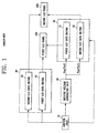
- FIG. 1 is a block diagram of a configuration driving a conventional dual type LCD panel
- FIG. 2A is a plan view illustrating a wiring status of the conventional dual type LCD display device.
- the conventional dual type LCD display device includes an LCD gate driver 30 and an LCD data driver 40.
- the LCD gate driver 30 comprises a first LCD gate driver 31 and a second LCD gate driver 32 to drive a first LCD panel 100 and a a second LCD panel 200, respectively.
- the data driver 40 comprises a first LCD data driver 41 and a second LCD data driver 42 corresponding to the first LCD panel 100 and the second LCD panel 200, respectively.
- a voltage from a control unit 10 is applied to a driving voltage generating unit 20, and a voltage signal from the driving voltage generating unit 20 is applied to the LCD gate driver 30.
- a gate driving voltage is received from the control unit 10, and thus a gate signal is applied to scan lines.
- the first LCD gate driver 31 maintains a Von state while the second LCD gate driver 32 maintains a Voff state.
- the control unit 10 applies a data signal only to the first LCD data driver 41 to drive the first LCD panel 100.
- the driving voltage generating unit 20 allows a gate driving voltage of the first LCD gate driver 31 to be maintained in a Voff state, and a gate driving voltage of the second LCD gate driver 32 to be maintained in a Von state.
- a data signal is applied only to the second LCD data driver 42 in the LCD data driver 40 to drive the second LCD 200.
- the LCD gate and data drivers 30 and 40 comprise the second LCD gate driver 32, it is not necessary for the dual type LCD panel to also comprise the second LCD data driver 42. Similarly, if the LCD gate and data drivers 30 and 40 comprise the second LCD data driver 42, it is not necessary for the dual type LCD panel to also comprise the LCD gate driver 32. That is, the LCD gate and data drivers 30 and 40 may comprise only one of the second LCD gate driver 32 and the second LCD data driver 42.
- the conventional art has a disadvantage in that, since a need exists for wirings LSn+1 through LS2n and LDn+1 through LD2n extending from the second LCD gate driver 32 and the second LCD data driver 42, respectively, to the second LCD panel 200, as well as wirings LS1 through LSn and LD1 through LDn extending from the first LCD gate driver 31 and the first LCD data driver 41, respectively, to the first LCD panel 100,as shown in FIG. 2, there exists a margin, namely, a dead space where the wiring for the second LCD panel 200 is disposed, which increases the size of the dual type LCD display device.
- Korean Laid-Open Patent Nos. 2001-974 and 2003-37126 describe a folder type mobile phone with a dual LCD panel.
- a dual type LCD composed of first and second LCDs is used for internal and external windows of the mobile phone, and comprises one LCD driving unit or two driving units for driving the first and second LCDs.
- An aspect of the present invention is to provide a dual type flat panel display device which can be compactly manufactured by designing a gate and/or data signal source into one chip without increasing a dead space in fabricating the display device, and which can reduce manufacturing cost because of its simple configuration.
- a dual type flat panel display device comprising: a first flat panel display device panel; and a second flat panel display device panel; wherein the first and second flat panel display device panels each include: a pixel area including a plurality of scan lines arranged in a first direction, a plurality of data lines arranged in a second direction perpendicular to the first direction, and pixel electrodes disposed in an area formed by the plurality of data lines and the plurality of scan lines crossing the data lines; and a non-pixel area including a plurality of on/off switching devices at inputs of the scan lines or the data lines, wherein the switching devices are respectively connected to the plurality of scan lines or the plurality of data lines.
- a dual type flat panel display device comprising: first and second flat panel display device panels including a plurality of scan lines, a plurality of data lines, and a plurality of pixel electrodes; a gate driver to output a gate driving signal and a gate driving voltage to the plurality of scan lines; a data driver to output a driving voltage to the plurality of data lines according to a received data driver driving signal; a control unit to generate the data driver driving signal and the gate driving signal; a driving voltage generating unit to receive the gate driving signal from the control unit and output the gate driving voltage to the gate driver; and on/off switching devices respectively connected to either the plurality of scan lines or the plurality of data lines.
- the present invention relates to a dual flat panel display device which includes a first flat panel display device panel and a second flat panel display device panel.
- these flat panel display device panels are LCD panels, but the present invention is not limited to such.
- organic electroluminescence display panels, as well as other types of display panels may be used.
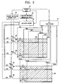
- FIG. 3 is a plan view illustrating a wiring status of a dual type LCD display device according to an embodiment of the present invention.
- a dual type LCD display device includes a first LCD panel 100 and a second LCD panel 200.
- the first LCD panel 100 and the second LCD panel 200 include a plurality of scan lines LS1, LS2,..., LSn arranged in a first direction.
- the first LCD panel 100 also includes a plurality of data lines LD1, LD2,...,LDn-1, LDn arranged in a second direction perpendicular to the first direction
- the second LCD panel 200 also includes a plurality of data lines LDn+1, LDn+2,..., LD2n-1, LD2n arranged in the second direction perpendicular to the first direction.
- the first LCD panel 100 and the second LCD panel 200 each include a pixel area, including pixel electrodes formed in the pixel area, which is formed by the plurality of data lines LD1, LD2,...,LDn-1, LDn, and LDn+1, LDn+2,..., LD2n-1 and LD2n, respectively, and the plurality of scan lines LS1, LS2,...., LSn crossing the data lines.
- a plurality of on/off switching devices S11, S12,..., S1n and S21, S22,..., S2n are included in inputs of the scan lines LS1, LS2,..., LSn of the first LCD panel 100 and the second LCD panel 200.
- the plurality scan lines LS1, LS2,...,LSn of the first LCD panel 100 and the plurality scan lines LS1, LS2,...,LSn of the second LCD panel 200 are respectively interconnected by common wirings.
- the total number of the wirings required to implement the dual type flat panel display device in the conventional case illustrated in FIG. 2 is 2n. But in this embodiment of the present invention, the number of necessary wirings is only n. As a result, the number of the wirings is reduced.
- the first LCD panel 100 and the second LCD panel 200 are simultaneously provided driving signals.
- the dual type flat panel display device it is required in the dual type flat panel display device that when the first LCD panel 100 is driven, the second LCD panel 200 is not driven. Similarly, it is required that when the second LCD panel 200 is driven, the first LCD panel 100 is not driven.
- this embodiment of the present invention comprises the on/off switching devices 50, including S11, S12,..., S1n and S21, S22,...,S2n, corresponding to respective gate signal inputs, enabling the switching devices S11 to S1n of the switching devices 50 to be in an ON state, while the switching devices S21 to S2n positioned at the inputs of the second LCD panel 200 to be in an OFF state, upon driving the first LCD panel 100.
- the switching devices S21 to S2n of the switching devices 50 are switched to be in an ON state, and the switching devices S11 to S1n of the switching devices 50, positioned at the inputs of the first LCD panel 100, are switched to be in an OFF state.
- the on/off switching devices 50 are formed of thin film transistors in which N or P type thin film transistors may be used for the thin film transistors.
- an on/off switching device control unit 60 may be further included.
- the on/off switching device control unit 60 can apply an electric signal to the on/off switching devices 50 to control an on/off state thereof.
- the on/off switching device control unit 60 can simultaneously control the on/off switching devices 50 in the first LCD panel 100 or the second LCD panel 200 with only one signal.
- the first LCD panel 100 and the second LCD panel 200 do not have to separately include the first and second LCD gate drivers 31 and 32 and the first and second LCD data drivers 41 and 42 to generate and apply a gate signal and a data signal, respectively.
- One LCD gate driver 30 and one LCD data driver 40 can selectively drive the first LCD panel 100 and the second LCD panel 200 without the separate first and second gate and data drivers 31, 32, 41, and 42, thereby reducing the number of the drivers as compared to the conventional art.
- the present invention can be also applied to the data lines.
- the scan lines should be formed individually for each of the first LCD panel 100 and the second LCD panel 200.
- one or more switching devices are included per an area (pixel area) surrounded by the scan lines LS1, LS2,..., LSn and the data lines LD1, LD2,...,LDn-1, LDn and LDn+1, LDn+2,..., LD2n-1, LD2n.
- the thin film transistors maintain an on/off state according to gate driving voltages applied to gate electrodes G of the thin film transistors via the scan lines. Further, data signals (image signals) are received via the data lines and source electrodes S of the thin film transistors from the LCD data driver 40, and are delivered to pixel electrodes via drain electrodes D of the thin film transistors, thereby generating light in the flat panel display devices in the pixel areas.
- the thin film transistors be P or N type thin film transistors.
- the number of the wirings is reduced as compared to the conventional art even while implementing the dual type flat panel display device. Further, the number of the drivers is reduced, thereby saving manufacturing cost, and a dead space is reduced, thereby more compactly manufacturing the display device.
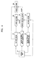
- FIG. 4 is a block diagram of a configuration for driving a dual type LCD panel according to an embodiment of the present invention.
- a flat panel display device of the present invention includes a control unit 10, a driving voltage generating unit 20, an LCD gate driver 30, an LCD data driver 40, on/off switching devices 50, and a first LCD panel 100 and a second LCD panel 200.
- the control unit 10 outputs to the driving voltage generating unit 20 a signal defining the period and amplitude of a common voltage applied to the first and second LCD panels 100 and 200, outputs a data driver driving signal to the LCD data driver 40, and outputs a gate driver driving signal to the LCD gate driver 30 according to a vertical synchronization signal, a horizontal synchronization signal, and a main clock signal applied from outside the the control unit.
- the data driver 40 outputs a data driving voltage to respective data lines of the first LCD panel 100 and the second LCD panel 200 in response to the data driver driving signal.
- the driving voltage generating unit 20 receives a signal defining the period and amplitude of a common electrode voltage Vcom from the control unit to adjust a voltage level of the signal up or down, and outputs a gate driving voltage Von or Voff to the LCD gate driver 30.
- the gate driver 30 outputs a gate driving voltage to the LCD panels 100 and 200, based on the gate driver driving signal provided from the control unit 10 and the gate driving voltage Von or Voff provided from the driving voltage generating unit 20.
- the on/off switching devices 50 are connected to either the scan line inputs or the data line inputs, and are correspondingly connected to the scan lines or the data lines, respectively.
- the switching devices 50 connected to the first LCD panel 100 are place in an ON state, and the switching devices 50 connected to the second LCD panel 200 are placed in an OFF state, so that a driving voltage signal outputted from the LCD gate driver 30 to the LCD panels 100 and 200 is applied only to the first LCD panel 100, thereby driving only the first LCD panel 100.
- an electric signal is received from the on/off switching device control unit 60 so that the switching devices 50 connected to the first LCD panel 100 maintain an OFF state, and the switching devices 50 connected to the second LCD panel 200 maintain an ON state, thereby driving only the second LCD flat panel display device panel 200.
- the first and second LCD panels 100 and 200 comprise a plurality of scan lines, a plurality of data lines, and a plurality of common electrode lines, thin film transistors connected to respective scan lines and data lines, liquid crystal capacitors, and storage capacitors. Accordingly, the first and second LCD panels 100 and 200 will display a data voltage (or an image signal) provided from the LCD data driver 40 in response to a gate voltage (or a scan signal) provided from the LCD gate driver 30 and a common electrode voltage provided from the driving voltage generating unit 20.
- the 1 st through n th scan or data line of the first LCD panel 100 and the 1 st through n th scan or data line of the second LCD panel 200 are interconnected by one wiring.
- the first LCD panel 100 and the second LCD panel 200 do not have to separately include the first and second LCD gate drivers 31 and 32 and the first and second LCD data drivers 41 and 42 to drive a scan signal (gate driving signal) and a data signal (image signal), respectively, and the number of the wirings is also reduced.
- the first flat panel display device panel 100 and the second LCD panel 200 can be selectively driven only with one LCD gate driver 30 and one LCD data driver 40.
- N or P type thin film transistors are used for the on/off switching devices 50.
- a dual type flat panel display device of the present invention can be applied to all flat panel display devices, and can be used for an organic electroluminescent element or a liquid crystal display device, in which the liquid crystal display device may include a super twisted nematic liquid crystal display device, a TFT liquid crystal display device, a field sequential liquid crystal display device, or the like.
- the number of the wirings is reduced as compared to the conventional art when implementing a dual type flat panel display device. Further, the manufacturing cost is lowered as the number of the driving drivers is reduced, and a display device can be manufactured more compactly as the dead space is reduced.
Landscapes
- Engineering & Computer Science (AREA)
- Chemical & Material Sciences (AREA)
- Crystallography & Structural Chemistry (AREA)
- Physics & Mathematics (AREA)
- Computer Hardware Design (AREA)
- General Physics & Mathematics (AREA)
- Theoretical Computer Science (AREA)
- Liquid Crystal (AREA)
- Devices For Indicating Variable Information By Combining Individual Elements (AREA)
- Control Of Indicators Other Than Cathode Ray Tubes (AREA)
- Liquid Crystal Display Device Control (AREA)
Applications Claiming Priority (2)
| Application Number | Priority Date | Filing Date | Title |
|---|---|---|---|
| KR1020040008500A KR100611164B1 (ko) | 2004-02-09 | 2004-02-09 | 듀얼형 평판 표시 디스플레이 소자 및 듀얼형 평판 표시 디스플레이 장치 |
| KR2004008500 | 2004-02-09 |
Publications (2)
| Publication Number | Publication Date |
|---|---|
| EP1562169A2 true EP1562169A2 (de) | 2005-08-10 |
| EP1562169A3 EP1562169A3 (de) | 2008-07-23 |
Family
ID=34676021
Family Applications (1)
| Application Number | Title | Priority Date | Filing Date |
|---|---|---|---|
| EP04090358A Ceased EP1562169A3 (de) | 2004-02-09 | 2004-09-16 | Doppel-Flachbildanzeige |
Country Status (5)
| Country | Link |
|---|---|
| US (1) | US7755565B2 (de) |
| EP (1) | EP1562169A3 (de) |
| JP (1) | JP4589677B2 (de) |
| KR (1) | KR100611164B1 (de) |
| CN (1) | CN100587570C (de) |
Cited By (1)
| Publication number | Priority date | Publication date | Assignee | Title |
|---|---|---|---|---|
| CN100353403C (zh) * | 2006-02-09 | 2007-12-05 | 友达光电股份有限公司 | 有机发光显示器 |
Families Citing this family (20)
| Publication number | Priority date | Publication date | Assignee | Title |
|---|---|---|---|---|
| JP4139786B2 (ja) * | 2004-02-17 | 2008-08-27 | シャープ株式会社 | 表示装置およびその駆動方法 |
| KR20060070346A (ko) * | 2004-12-20 | 2006-06-23 | 삼성전자주식회사 | 표시 장치 |
| KR20070082335A (ko) * | 2006-02-16 | 2007-08-21 | 엘지전자 주식회사 | 정보 처리 장치 |
| JP2008077008A (ja) * | 2006-09-25 | 2008-04-03 | Casio Comput Co Ltd | 表示装置 |
| KR100807017B1 (ko) * | 2007-01-17 | 2008-02-25 | 삼성에스디아이 주식회사 | 휴대용 전자기기 |
| US8248352B2 (en) | 2008-04-25 | 2012-08-21 | Lg Display Co., Ltd. | Driving circuit of liquid crystal display |
| KR101408260B1 (ko) * | 2008-04-25 | 2014-06-18 | 엘지디스플레이 주식회사 | 액정표시장치의 게이트 구동 회로 |
| TWI393046B (zh) * | 2008-10-23 | 2013-04-11 | Chun Wei Chu | 雙顯示螢幕可攜式電子閱讀器與作業系統 |
| TWI420362B (zh) * | 2010-04-19 | 2013-12-21 | Au Optronics Corp | 觸控面板 |
| CN102446498B (zh) * | 2010-10-12 | 2013-08-07 | 北京京东方光电科技有限公司 | 液晶显示器的驱动装置和驱动方法 |
| CN103247276B (zh) * | 2013-04-25 | 2015-03-18 | 北京京东方光电科技有限公司 | 栅极驱动电路和阵列基板 |
| WO2015075844A1 (ja) * | 2013-11-20 | 2015-05-28 | パナソニック液晶ディスプレイ株式会社 | 表示装置 |
| KR102169459B1 (ko) | 2013-12-06 | 2020-10-26 | 삼성디스플레이 주식회사 | 표시 장치 및 멀티 패널 표시 장치 |
| KR102293456B1 (ko) * | 2015-04-17 | 2021-08-27 | 삼성디스플레이 주식회사 | 표시 패널 |
| JP6830765B2 (ja) * | 2015-06-08 | 2021-02-17 | 株式会社半導体エネルギー研究所 | 半導体装置 |
| KR20180000771A (ko) * | 2016-06-23 | 2018-01-04 | 삼성디스플레이 주식회사 | 표시 장치 |
| KR102665178B1 (ko) * | 2016-09-21 | 2024-05-14 | 삼성디스플레이 주식회사 | 표시 장치 및 그의 제조 방법 |
| CN106875890B (zh) * | 2017-04-27 | 2021-01-12 | 京东方科技集团股份有限公司 | 阵列基板、显示面板、显示设备及驱动方法 |
| CN109064986B (zh) * | 2018-08-29 | 2021-01-26 | 京东方科技集团股份有限公司 | 一种显示面板及其制作方法、驱动方法、显示装置 |
| CN111477150A (zh) * | 2020-04-30 | 2020-07-31 | 深圳市华星光电半导体显示技术有限公司 | 显示装置 |
Family Cites Families (19)
| Publication number | Priority date | Publication date | Assignee | Title |
|---|---|---|---|---|
| JP3282216B2 (ja) | 1992-07-03 | 2002-05-13 | カシオ計算機株式会社 | 入出力デバイスおよび入出力装置 |
| JPH10186396A (ja) | 1996-12-25 | 1998-07-14 | Canon Inc | 液晶装置 |
| JPH1117446A (ja) | 1997-06-27 | 1999-01-22 | Mitsubishi Electric Corp | アンテナ装置 |
| JP3229250B2 (ja) * | 1997-09-12 | 2001-11-19 | インターナショナル・ビジネス・マシーンズ・コーポレーション | 液晶表示装置における画像表示方法及び液晶表示装置 |
| JPH11174486A (ja) | 1997-12-16 | 1999-07-02 | Sony Corp | 液晶表示装置 |
| KR20010000974A (ko) | 1998-11-02 | 2001-01-05 | 윤종용 | 폴더형 휴대폰에서 양면 액정표시장치 |
| KR100444694B1 (ko) | 1999-08-04 | 2004-08-18 | 엘지전자 주식회사 | 폴더형 이동 통신 단말기의 표시장치 |
| JP2001356744A (ja) | 2000-06-16 | 2001-12-26 | Sharp Corp | 液晶表示装置および携帯用電子機器 |
| JP2003177684A (ja) * | 2001-09-21 | 2003-06-27 | Seiko Epson Corp | 電気光学パネル、電気光学装置及び電子機器 |
| KR100430593B1 (ko) | 2001-11-02 | 2004-05-10 | 삼성전자주식회사 | 듀얼 액정 표시 장치를 가지는 폴더형 휴대폰과 그휴대폰의 윈도우 화면 표시 제어 장치 및 제어 방법 |
| JP2003228336A (ja) | 2002-01-31 | 2003-08-15 | Toshiba Corp | 平面表示装置 |
| JP2003323164A (ja) | 2002-05-08 | 2003-11-14 | Hitachi Displays Ltd | 液晶表示装置とその駆動方法 |
| JP4794801B2 (ja) | 2002-10-03 | 2011-10-19 | ルネサスエレクトロニクス株式会社 | 携帯型電子機器の表示装置 |
| JP4145637B2 (ja) * | 2002-11-25 | 2008-09-03 | シャープ株式会社 | アクティブマトリクス基板及び表示装置 |
| KR101019138B1 (ko) | 2002-12-27 | 2011-03-04 | 가부시키가이샤 한도오따이 에네루기 켄큐쇼 | 표시장치 및 전자기기 |
| US7385598B2 (en) * | 2003-06-27 | 2008-06-10 | Samsung Electronics, Co., Ltd. | Driver for operating multiple display devices |
| JP2005055467A (ja) | 2003-08-01 | 2005-03-03 | Sharp Corp | 表示装置 |
| JP4703955B2 (ja) | 2003-09-10 | 2011-06-15 | 株式会社 日立ディスプレイズ | 表示装置 |
| KR100957574B1 (ko) * | 2003-09-17 | 2010-05-11 | 삼성전자주식회사 | 표시장치 |
-
2004
- 2004-02-09 KR KR1020040008500A patent/KR100611164B1/ko not_active Expired - Lifetime
- 2004-08-04 JP JP2004228140A patent/JP4589677B2/ja not_active Expired - Lifetime
- 2004-08-25 US US10/924,911 patent/US7755565B2/en active Active
- 2004-09-16 EP EP04090358A patent/EP1562169A3/de not_active Ceased
- 2004-09-27 CN CN200410082679A patent/CN100587570C/zh not_active Expired - Lifetime
Cited By (1)
| Publication number | Priority date | Publication date | Assignee | Title |
|---|---|---|---|---|
| CN100353403C (zh) * | 2006-02-09 | 2007-12-05 | 友达光电股份有限公司 | 有机发光显示器 |
Also Published As
| Publication number | Publication date |
|---|---|
| JP2005222015A (ja) | 2005-08-18 |
| CN1655037A (zh) | 2005-08-17 |
| CN100587570C (zh) | 2010-02-03 |
| US7755565B2 (en) | 2010-07-13 |
| JP4589677B2 (ja) | 2010-12-01 |
| US20050174299A1 (en) | 2005-08-11 |
| EP1562169A3 (de) | 2008-07-23 |
| KR20050080411A (ko) | 2005-08-12 |
| KR100611164B1 (ko) | 2006-08-09 |
Similar Documents
| Publication | Publication Date | Title |
|---|---|---|
| US7755565B2 (en) | Dual type flat panel display device | |
| US7948461B2 (en) | Image display device | |
| JP4072332B2 (ja) | 液晶表示装置およびその駆動方法 | |
| KR100462133B1 (ko) | 표시 장치 | |
| TWI383361B (zh) | 驅動電路、液晶裝置、電子機器及液晶裝置之驅動方法 | |
| US20120274623A1 (en) | Display apparatus and method of driving the same | |
| KR20010062655A (ko) | 표시 장치 | |
| US9691343B2 (en) | Display device comprising display panel with bridge patterns | |
| EP2360671A1 (de) | Flüssigkristallanzeige und Ansteuerverfahren dafür | |
| US8054393B2 (en) | Liquid crystal display device | |
| WO2011125416A1 (ja) | 液晶表示装置 | |
| JP2012088736A (ja) | 表示装置 | |
| US20130107153A1 (en) | Thin film transistor array structure and liquid crystal panel using the same | |
| KR100700645B1 (ko) | 액정 표시 장치 및 그의 구동방법 | |
| US7358955B2 (en) | Liquid crystal display for mobile phone | |
| JP2010250265A (ja) | 液晶表示装置および電子機器 | |
| JP5004386B2 (ja) | 表示装置及びその駆動方法 | |
| JP2008102242A (ja) | 電気光学装置、駆動回路および電子機器 | |
| US8704746B2 (en) | Liquid crystal display having a voltage stabilization circuit and driving method thereof | |
| US8310429B2 (en) | Discharge circuit and liquid crystal display using the same | |
| KR100623713B1 (ko) | 액정 표시 장치 및 그의 구동방법 | |
| JP2002162947A (ja) | 表示装置 | |
| JP3668115B2 (ja) | 表示装置 | |
| KR100623249B1 (ko) | 듀얼형 액정 표시 디스플레이 소자 | |
| KR100469193B1 (ko) | 표시 장치 |
Legal Events
| Date | Code | Title | Description |
|---|---|---|---|
| PUAI | Public reference made under article 153(3) epc to a published international application that has entered the european phase |
Free format text: ORIGINAL CODE: 0009012 |
|
| AK | Designated contracting states |
Kind code of ref document: A2 Designated state(s): AT BE BG CH CY CZ DE DK EE ES FI FR GB GR HU IE IT LI LU MC NL PL PT RO SE SI SK TR |
|
| AX | Request for extension of the european patent |
Extension state: AL HR LT LV MK |
|
| PUAL | Search report despatched |
Free format text: ORIGINAL CODE: 0009013 |
|
| AK | Designated contracting states |
Kind code of ref document: A3 Designated state(s): AT BE BG CH CY CZ DE DK EE ES FI FR GB GR HU IE IT LI LU MC NL PL PT RO SE SI SK TR |
|
| AX | Request for extension of the european patent |
Extension state: AL HR LT LV MK |
|
| 17P | Request for examination filed |
Effective date: 20081201 |
|
| RAP1 | Party data changed (applicant data changed or rights of an application transferred) |
Owner name: SAMSUNG MOBILE DISPLAY CO., LTD. |
|
| 17Q | First examination report despatched |
Effective date: 20090211 |
|
| AKX | Designation fees paid |
Designated state(s): DE FR GB |
|
| STAA | Information on the status of an ep patent application or granted ep patent |
Free format text: STATUS: THE APPLICATION HAS BEEN REFUSED |
|
| 18R | Application refused |
Effective date: 20111108 |