EP1561339B1 - Read-out circuit for infrared detectors - Google Patents
Read-out circuit for infrared detectors Download PDFInfo
- Publication number
- EP1561339B1 EP1561339B1 EP03775001.5A EP03775001A EP1561339B1 EP 1561339 B1 EP1561339 B1 EP 1561339B1 EP 03775001 A EP03775001 A EP 03775001A EP 1561339 B1 EP1561339 B1 EP 1561339B1
- Authority
- EP
- European Patent Office
- Prior art keywords
- input
- read
- switch
- capacitor
- out circuit
- Prior art date
- Legal status (The legal status is an assumption and is not a legal conclusion. Google has not performed a legal analysis and makes no representation as to the accuracy of the status listed.)
- Expired - Lifetime
Links
- 239000003990 capacitor Substances 0.000 claims description 46
- 238000001514 detection method Methods 0.000 claims description 8
- 230000010354 integration Effects 0.000 description 14
- 238000012937 correction Methods 0.000 description 12
- 239000000243 solution Substances 0.000 description 8
- 238000013461 design Methods 0.000 description 5
- 238000000034 method Methods 0.000 description 5
- 230000007850 degeneration Effects 0.000 description 4
- 230000000694 effects Effects 0.000 description 4
- 238000006243 chemical reaction Methods 0.000 description 2
- 230000008878 coupling Effects 0.000 description 2
- 238000010168 coupling process Methods 0.000 description 2
- 238000005859 coupling reaction Methods 0.000 description 2
- 238000002347 injection Methods 0.000 description 2
- 239000007924 injection Substances 0.000 description 2
- 230000002441 reversible effect Effects 0.000 description 2
- 238000005070 sampling Methods 0.000 description 2
- 238000013459 approach Methods 0.000 description 1
- 230000002238 attenuated effect Effects 0.000 description 1
- 239000007795 chemical reaction product Substances 0.000 description 1
- 230000002596 correlated effect Effects 0.000 description 1
- 230000009977 dual effect Effects 0.000 description 1
- 238000009413 insulation Methods 0.000 description 1
- 230000007774 longterm Effects 0.000 description 1
- 230000035945 sensitivity Effects 0.000 description 1
- 230000006641 stabilisation Effects 0.000 description 1
- 230000009897 systematic effect Effects 0.000 description 1
- 238000012546 transfer Methods 0.000 description 1
Images


Classifications
-
- H—ELECTRICITY
- H03—ELECTRONIC CIRCUITRY
- H03F—AMPLIFIERS
- H03F3/00—Amplifiers with only discharge tubes or only semiconductor devices as amplifying elements
- H03F3/04—Amplifiers with only discharge tubes or only semiconductor devices as amplifying elements with semiconductor devices only
- H03F3/08—Amplifiers with only discharge tubes or only semiconductor devices as amplifying elements with semiconductor devices only controlled by light
- H03F3/087—Amplifiers with only discharge tubes or only semiconductor devices as amplifying elements with semiconductor devices only controlled by light with IC amplifier blocks
-
- H—ELECTRICITY
- H03—ELECTRONIC CIRCUITRY
- H03F—AMPLIFIERS
- H03F3/00—Amplifiers with only discharge tubes or only semiconductor devices as amplifying elements
- H03F3/45—Differential amplifiers
- H03F3/45071—Differential amplifiers with semiconductor devices only
- H03F3/45479—Differential amplifiers with semiconductor devices only characterised by the way of common mode signal rejection
- H03F3/45928—Differential amplifiers with semiconductor devices only characterised by the way of common mode signal rejection using IC blocks as the active amplifying circuit
- H03F3/45968—Differential amplifiers with semiconductor devices only characterised by the way of common mode signal rejection using IC blocks as the active amplifying circuit by offset reduction
- H03F3/45973—Differential amplifiers with semiconductor devices only characterised by the way of common mode signal rejection using IC blocks as the active amplifying circuit by offset reduction by using a feedback circuit
- H03F3/45977—Differential amplifiers with semiconductor devices only characterised by the way of common mode signal rejection using IC blocks as the active amplifying circuit by offset reduction by using a feedback circuit using switching means, e.g. sample and hold
-
- H—ELECTRICITY
- H04—ELECTRIC COMMUNICATION TECHNIQUE
- H04N—PICTORIAL COMMUNICATION, e.g. TELEVISION
- H04N25/00—Circuitry of solid-state image sensors [SSIS]; Control thereof
- H04N25/60—Noise processing, e.g. detecting, correcting, reducing or removing noise
- H04N25/67—Noise processing, e.g. detecting, correcting, reducing or removing noise applied to fixed-pattern noise, e.g. non-uniformity of response
- H04N25/671—Noise processing, e.g. detecting, correcting, reducing or removing noise applied to fixed-pattern noise, e.g. non-uniformity of response for non-uniformity detection or correction
-
- H—ELECTRICITY
- H04—ELECTRIC COMMUNICATION TECHNIQUE
- H04N—PICTORIAL COMMUNICATION, e.g. TELEVISION
- H04N5/00—Details of television systems
- H04N5/30—Transforming light or analogous information into electric information
- H04N5/33—Transforming infrared radiation
-
- H—ELECTRICITY
- H03—ELECTRONIC CIRCUITRY
- H03F—AMPLIFIERS
- H03F2200/00—Indexing scheme relating to amplifiers
- H03F2200/261—Amplifier which being suitable for instrumentation applications
Definitions
- the present invention is related to low offset, low noise auto-zeroed CMOS integrated circuit amplifiers and more in particular to read-out circuits for infrared detectors.
- a focal plane array comprises several individual detector elements (pixels). The number of pixels in a linear or focal plane array is increasing.
- the signal multiplexer is a high complexity detector specific integrated circuit, which reads all channels in parallel.
- the most commonly used detector circuits are the direct injection stage and the capacitive feedback transimpedance amplifier (CTIA).
- a conventional detector buffer stage in a read-out circuit comprises a capacitive feedback transimpedance amplifier.
- the goal of the CTIA is to accumulate all detector current, preferably under the condition of zero bias or some reverse bias where the dynamic resistance is high.
- the amplifier keeps the detector at virtual ground while the detector current is flowing onto the capacitor, generating a voltage signal at the output proportional to the integration time and the signal current.
- the DC coupling between the detector and the CTIA yields an excellent linearity of the detector current to output voltage conversion. In the ideal condition of zero offset there is no influence of dark current and hence of dark current noise. In this case the detector shunt resistance does not play a role as there is no voltage difference over the detector.
- Patent US-A-6087897 relates to an offset and non-linearity compensated amplifier and method. It discloses a normal voltage amplifier with a feedback network, wherein the ratio C 1 /C 2 defines the voltage gain V out /V in .
- the circuit comprises a capacitor C3 whereon the previous value of the amplifier output voltage is stored. This assures the amplifier output voltage and the operating voltage to be close to one another during autozero, which permits a low gain.
- the output voltage does not vary significantly between autozero phase and normal operation phase, which basically limits usefulness of this circuit to relatively slow voltage signals as compared to the switching frequency.
- the present invention aims to provide a low noise, high uniformity auto-zeroed integrated circuit amplifier overcoming the problems of the prior art solution. More specifically it provides a read-out circuit for infrared detectors.
- the present invention is related to a device according to claim 1 comprising a capacitive feedback transimpedance operational amplifier, that comprises a main operational amplifier (with a first input, a second input and an output) and an integrating capacitor, connected between the second input and the output, and a first switch connected in parallel to the integrating capacitor.
- the device further comprises an auto-zero operational amplifier having a third input and a fourth input, whereby to the third input and the first input signals at virtual ground potential are applied.
- the fourth input is connected to the output by a circuit comprising two offset error capacitors, a second switch and a third switch.
- the offset error capacitors have a terminal connected to the virtual ground potential
- the auto-zero operational amplifier comprises resistor connected MOS transistors.
- the second and the third switch each comprise four transistors.
- the integrating capacitor comprises a plurality of capacitors in parallel, whereby in each parallel branch an isolating switch is provided on either side of the capacitor in said branch.
- Typically said output is further connected to a sample&hold circuit.
- a read-out circuit for infrared detection comprises a plurality of devices as described above.
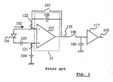
- FIG. 1 shows a prior art detector bluffer stage, consisting of a charge sensitive transimpedance amplifier (CTIA) (11).
- CTIA charge sensitive transimpedance amplifier
- the CTIA accumulates all detector current 102, preferably under zero bias or some reverse bias 103 where the dynamic resistance is high. However one always has to deal with a varying offset voltage. Therefore when applying CMOS amplifiers it is common to use an auto-zero (AZ) circuit.
- AZ auto-zero
- the system exhibits an excellent linearity of the detector current 102 to output voltage conversion due to the DC coupling between the infrared detector diode 101 and the low equivalent input impedance presented at the differential inputs - (122) and + (121) of the main amplifier 107 and its integrating capacitor 106 combination forming the CTIA (11).
- the non-uniformity of the input offset voltage of the individual op-amps in a focal plane array gives rise to so called fixed pattern noise on an array of such read-outs and limits the integration time
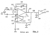
- Fig. 2 shows a modified version of the above schematic based on an auxiliary Auto-Zero (AZ) op-amp, which corrects for the above described anomaly.
- the scheme shows a dual op-amp design, where the AZ op-amp 110 is used to reduce the offset effects of the main CTIA stage 11.
- This correcting AZ opamp 110 is known to provide a certain transconductance attenuation as compared to the main op-amp 107 by the introduction of source degeneration resistors 408 and 409 (see also Fig.4 ).
- each CTIA is auto-zeroed again by closing simultaneously the AZ switch 111 and switch 115 and opening the optional switch 116.
- the correction coefficient is stored on the capacitor 112 of the auxiliary amplifier 110 by first opening the switch 111. Then the CTIA main op-amp 107 and its integration capacitor 106 are reset to the virtual zero start point by closing switch 105 during a short time. Then the real integration cycle starts and it ends with the sampling (by closing switch 108) and holding (by opening switch 108) the amplifiers output voltage resulting from the integrated detector current signal on the S&H capacitor 109. Finally all acquired information stored on the hold capacitors 109 of an array of identical circuits is read out by applying a start pulse to the selection shift register.
- This register sequentially selects each channel's output 118 buffered by a follower amplifier 117 and directs its output signal to a common output buffer amplifier generating a so called video signal.
- This signal can be visualised on a video display screen to give an image of the signals detected by the infrared diode array.
- the auto-zero scheme of Fig. 2 is known within the electronics community.
- the scheme of Fig.3 however comprises a combination of novel features that cannot be found in prior art solutions.
- the amplifier's common mode rejection is used to attenuate noise.
- the AZ amplifier is preferably not constructed as an independent circuit block, but is embedded in the first stage of the principal CTIA op-amp (as shown in Fig.4 and 5 ). It is designed in such a way that it corrects the current flowing in the principal op-amp 107 to approach better the virtual ground potential 104.
- US 4884039 also uses an embedded solution, but there the external capacitor is not differentially coupled.
- a differential amplifier is more sensitive to a differential voltage at its inputs than a so called common-mode voltage (i.e.
- the error correction voltage stored in the Auto-Zero correction capacitor is directly connected across the differential inputs for which the amplifier is most sensitive.
- One of the terminals of the correction capacitor is connected to the virtual ground, which can be noisy or slowly varying. This is particularly the case since usually an externally provided voltage will be applied, as a common mode voltage to the amplifier's inputs, by virtue of the capacitor's principle to keep the voltage at its terminals constant.
- Fig.3 shows a novel means to achieve long integration time and yet keep very good linearity while keeping relatively small footprint requirements.
- a conventional AutoZero is performed with only one switch 111 and one error storage capacitor 112 (see also Fig.2 ).
- This has two important drawbacks.
- the amplifiers output dV/dt together with the MOS switch drain source stray capacitances and subtreshold or weak inversion current cause a small, but yet non-negligible current to flow into the storage capacitor 112.
- This causes the stored error voltage to vary slightly, which gives rise to an output non-linearity, particularly at long integration times, or with small integration capacitor value or both, thus when the system is most sensitive to input current and hence to offset errors.
- By providing a second capacitor 114 and switch 113 a much better insulation from the amplifiers output dV/dt is ensured, because of the very low voltage difference across the second switch 113.
- the switches are designed to minimise the charge injection on both sides of the switches, thereby also minimising the systematic offset error.
- compensation is impossible to achieve, as transistors of different size are required, and so process variations will cause unpredictable ratios between the effective transistor sizes.
- the capacitors are directly connected across the differential inputs of the correcting amplifier 110 as already discussed before.
- Fig.4 shows more in detail the combined main and AZ op-amp including the so called source degeneration resistors 408 and 409.
- Fig.4 shows a solution with PMOS differential input transistors, but to a person skilled in the art it is clear that this is just an example of a possible implementation and that a scheme with all transistors types and supply polarities inverted has exactly the same basic function.
- the correction differential input pair's source degeneration resistors 408-409 in Fig.4 can be alternatively replaced by resistor connected MOS transistors 508-509 as shown in a detailed alternative schematic in Fig.5 .
- the MOS transistors modify the transfer characteristics in such a way that a much lower transconductance is obtained. Furthermore said transconductance is nearly linear over a much wider voltage range than a conventional MOS input pair. In this way, all imperfections of the offset compensation voltage are also reduced in the same ratio as the transconductances ratio between primary and secondary correction input pair. Also large offset voltage errors can still be captured and corrected, resulting in an overall better end product yield and guaranteed long term operation.
- the use of said resistor connected MOS transistors additionally offers the considerable advantage of being applicable in all CMOS processes.
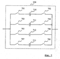
- FIG. 7 which is a detail of a possible implementation of the integration capacitor 106 in Fig. 3
- the different capacitors 710 to 713 are of different values to allow to change the value of the total capacitor connected across the amplifiers feedback in order to modify the sensitivity of the resulting integrator. It is obvious that the number of capacitors and their value will vary from design to design depending on the range and values of transimpedance value (or gain) required.
- the capacitors are not single sided switched, but double sided (see switches 701 to 708). This measure allows to fully isolate the capacitor from its environment and to execute other charge domain operations without affecting the information charge on the (switched off) feedback capacitors.
- This last feature is necessary to introduce the multiple AZ concept.
- the feedback capacitors are switched off from the CTIA amplifier. At that moment a new AZ operation is executed and then the feedback capacitor is again connected to the CTIA to continue the integration cycle.
- the effect of this multiple AZ scheme is that in effect it will average the noise voltage of the successive AZ' s. This is because despite all means used to minimise noise, there will always remain a small amount of it in the stored auto-zero correction voltage so that successive readings of the same small infrared diode current will result in possibly relatively large errors in the successive integrated output voltage values.
Applications Claiming Priority (3)
| Application Number | Priority Date | Filing Date | Title |
|---|---|---|---|
| US42503602P | 2002-11-07 | 2002-11-07 | |
| US425036P | 2002-11-07 | ||
| PCT/BE2003/000187 WO2004043062A1 (en) | 2002-11-07 | 2003-11-06 | Read-out circuit for infrared detectors. |
Publications (2)
| Publication Number | Publication Date |
|---|---|
| EP1561339A1 EP1561339A1 (en) | 2005-08-10 |
| EP1561339B1 true EP1561339B1 (en) | 2015-10-21 |
Family
ID=32312919
Family Applications (1)
| Application Number | Title | Priority Date | Filing Date |
|---|---|---|---|
| EP03775001.5A Expired - Lifetime EP1561339B1 (en) | 2002-11-07 | 2003-11-06 | Read-out circuit for infrared detectors |
Country Status (7)
| Country | Link |
|---|---|
| US (1) | US7148727B2 (zh) |
| EP (1) | EP1561339B1 (zh) |
| JP (1) | JP4526949B2 (zh) |
| CN (1) | CN100525400C (zh) |
| AU (1) | AU2003283134A1 (zh) |
| CA (1) | CA2502467C (zh) |
| WO (1) | WO2004043062A1 (zh) |
Families Citing this family (32)
| Publication number | Priority date | Publication date | Assignee | Title |
|---|---|---|---|---|
| KR100656666B1 (ko) * | 2004-09-08 | 2006-12-11 | 매그나칩 반도체 유한회사 | 이미지 센서 |
| US7268607B2 (en) * | 2004-12-10 | 2007-09-11 | L-3 Communications Corporation | Integrating capacitance circuitry for an integrating amplifier and related method |
| JP2006222495A (ja) * | 2005-02-08 | 2006-08-24 | Olympus Corp | 光電流検出回路 |
| JP2006279377A (ja) | 2005-03-29 | 2006-10-12 | Handotai Rikougaku Kenkyu Center:Kk | チョッパ増幅回路 |
| US8294495B2 (en) | 2005-07-01 | 2012-10-23 | Maxim Integrated Products, Inc. | Constant slope ramp circuits for sampled-data circuits |
| US7486115B2 (en) * | 2005-07-01 | 2009-02-03 | Cambridge Analog Technologies, Inc. | Sampled-data circuits using zero crossing detection |
| US7522086B2 (en) | 2005-12-29 | 2009-04-21 | Cambridge Analog Technologies, Inc. | Reference circuits for sampled-data circuits |
| US7504866B2 (en) | 2005-12-29 | 2009-03-17 | Cambridge Analog Technologies, Inc. | Output hold circuits for sample-data circuits |
| KR100782304B1 (ko) * | 2006-02-03 | 2007-12-06 | 삼성전자주식회사 | Cds오프셋 보정 기능을 갖는 이미지 센서와이미지센서의 cds 방법 |
| US7411460B2 (en) * | 2006-03-10 | 2008-08-12 | Exar Corporation | Elimination of dummy detector on optical detectors using input common mode feedback |
| JP5292689B2 (ja) * | 2006-10-31 | 2013-09-18 | 日本電気株式会社 | 熱型赤外線撮像装置及びその動作方法 |
| US7525472B2 (en) * | 2006-12-27 | 2009-04-28 | Semiconductor Energy Laboratory Co., Ltd. | Integration type and converter and device including same |
| CN100510661C (zh) * | 2007-02-14 | 2009-07-08 | 中国科学院安徽光学精密机械研究所 | 反射式铟镓砷陷阱辐射探测器 |
| CN101425098B (zh) * | 2007-10-31 | 2010-08-25 | 中国科学院沈阳自动化研究所 | 红外探测器输出的模拟方法及装置 |
| WO2009157964A1 (en) * | 2008-06-26 | 2009-12-30 | Marshall Delph Earle | Techniques for monitoring storm conditions |
| GB2470214A (en) * | 2009-05-14 | 2010-11-17 | Powervation Ltd | Determining DC-DC converter losses |
| JP2011004327A (ja) * | 2009-06-22 | 2011-01-06 | Hamamatsu Photonics Kk | 積分回路および光検出装置 |
| JP5296612B2 (ja) * | 2009-06-22 | 2013-09-25 | 浜松ホトニクス株式会社 | 積分回路および光検出装置 |
| US8547170B1 (en) * | 2011-04-29 | 2013-10-01 | Bae Systems Information And Electronic Systems Integration Inc. | Multimode integration circuit for sensor readout |
| TWI439046B (zh) * | 2011-08-12 | 2014-05-21 | Richtek Technology Corp | 自動調零放大器及相關的偵測模組 |
| US8258864B1 (en) * | 2011-09-21 | 2012-09-04 | Hong Kong Applied Science And Technology Research Institute Co., Ltd. | Ultra low voltage multi-stage high-speed CMOS comparator with autozeroing |
| CN103036511B (zh) * | 2012-12-14 | 2015-06-03 | 电子科技大学 | 红外焦平面阵列探测器读出电路的adc余量放大电路 |
| TWI492538B (zh) | 2013-01-14 | 2015-07-11 | Univ Nat Chi Nan | Switchable reading device |
| JP6380882B2 (ja) * | 2013-06-17 | 2018-08-29 | セイコーNpc株式会社 | 信号検出回路 |
| GB2524521A (en) * | 2014-03-25 | 2015-09-30 | Voltech Instr Ltd | Apparatus and methods for measuring electrical current |
| JP6832649B2 (ja) | 2016-08-17 | 2021-02-24 | ブリルニクス インク | 固体撮像装置、固体撮像装置の駆動方法、および電子機器 |
| US10924701B2 (en) * | 2019-07-18 | 2021-02-16 | Omnivision Technologies, Inc. | Column amplifier reset circuit with comparator |
| JP7383500B2 (ja) | 2020-01-16 | 2023-11-20 | 浜松ホトニクス株式会社 | 固体撮像装置およびアンプアレイ |
| CN112738359A (zh) * | 2020-12-30 | 2021-04-30 | 长春长光辰芯光电技术有限公司 | Ctia像素单元 |
| FR3123121A1 (fr) | 2021-05-19 | 2022-11-25 | Stmicroelectronics (Grenoble 2) Sas | Capteur de lumiere ambiante |
| US11894670B2 (en) * | 2021-09-21 | 2024-02-06 | Raytheon Company | High-energy suppression for infrared imagers or other imaging devices |
| US11843355B2 (en) | 2022-02-04 | 2023-12-12 | Raytheon Company | High-energy suppression for capacitor transimpedance amplifier (CTIA)-based imagers or other imaging devices |
Family Cites Families (8)
| Publication number | Priority date | Publication date | Assignee | Title |
|---|---|---|---|---|
| US4047059A (en) * | 1976-05-24 | 1977-09-06 | Rca Corporation | Comparator circuit |
| US4978872A (en) * | 1984-12-17 | 1990-12-18 | Hughes Aircraft Company | Integrating capactively coupled transimpedance amplifier |
| JPH07105447B2 (ja) * | 1988-12-15 | 1995-11-13 | 株式会社東芝 | 伝送ゲート |
| US5043820A (en) * | 1989-03-27 | 1991-08-27 | Hughes Aircraft Company | Focal plane array readout employing one capacitive feedback transimpedance amplifier for each column |
| JP3625930B2 (ja) * | 1995-10-26 | 2005-03-02 | 株式会社日立製作所 | 半導体集積回路装置 |
| US5905398A (en) * | 1997-04-08 | 1999-05-18 | Burr-Brown Corporation | Capacitor array having user-adjustable, manufacturer-trimmable capacitance and method |
| US6087897A (en) * | 1999-05-06 | 2000-07-11 | Burr-Brown Corporation | Offset and non-linearity compensated amplifier and method |
| TW580568B (en) * | 2001-11-27 | 2004-03-21 | Matsushita Electric Works Ltd | An infrared detecting circuit and an infrared detector |
-
2003
- 2003-11-06 JP JP2004548946A patent/JP4526949B2/ja not_active Expired - Lifetime
- 2003-11-06 AU AU2003283134A patent/AU2003283134A1/en not_active Abandoned
- 2003-11-06 CN CNB2003801023640A patent/CN100525400C/zh not_active Expired - Lifetime
- 2003-11-06 WO PCT/BE2003/000187 patent/WO2004043062A1/en active Application Filing
- 2003-11-06 EP EP03775001.5A patent/EP1561339B1/en not_active Expired - Lifetime
- 2003-11-06 CA CA2502467A patent/CA2502467C/en not_active Expired - Lifetime
-
2005
- 2005-05-03 US US11/120,504 patent/US7148727B2/en not_active Expired - Lifetime
Non-Patent Citations (1)
| Title |
|---|
| CAIULO G ET AL: "Design of high-accuracy video comparator", CIRCUITS AND SYSTEMS, 1994. ISCAS '94., 1994 IEEE INTERNATIONAL SYMPOS IUM ON LONDON, UK 30 MAY-2 JUNE 1994, NEW YORK, NY, USA,IEEE, US LNKD- DOI:10.1109/ISCAS.1994.409113, vol. 3, 30 May 1994 (1994-05-30), pages 101 - 104, XP010143147, ISBN: 978-0-7803-1915-8 * |
Also Published As
| Publication number | Publication date |
|---|---|
| AU2003283134A1 (en) | 2004-06-07 |
| CA2502467C (en) | 2012-07-03 |
| CN1708983A (zh) | 2005-12-14 |
| US7148727B2 (en) | 2006-12-12 |
| CA2502467A1 (en) | 2004-05-21 |
| US20050199813A1 (en) | 2005-09-15 |
| WO2004043062A1 (en) | 2004-05-21 |
| CN100525400C (zh) | 2009-08-05 |
| EP1561339A1 (en) | 2005-08-10 |
| WO2004043062A8 (en) | 2004-11-04 |
| JP2006505975A (ja) | 2006-02-16 |
| JP4526949B2 (ja) | 2010-08-18 |
Similar Documents
| Publication | Publication Date | Title |
|---|---|---|
| EP1561339B1 (en) | Read-out circuit for infrared detectors | |
| US6906586B2 (en) | Differential amplifier circuit used in solid-state image pickup apparatus, and arrangement that avoids influence of variations of integrated circuits in manufacture and the like | |
| US7696817B1 (en) | Auto-gain correction and common mode voltage cancellation in a precision amplifier | |
| US6903670B1 (en) | Circuit and method for cancellation of column pattern noise in CMOS imagers | |
| US5963156A (en) | Sample and hold circuit and method with common mode differential signal feedback for converting single-ended signals to differential signals | |
| US7372392B1 (en) | Charge balancing method in a current input ADC | |
| US6952240B2 (en) | Image sampling circuit with a blank reference combined with the video input | |
| US4748418A (en) | Quasi auto-zero circuit for sampling amplifiers | |
| US7385426B1 (en) | Low current offset integrator with signal independent low input capacitance buffer circuit | |
| US11647312B2 (en) | Methods and apparatus for a track and hold amplifier | |
| US6700417B2 (en) | Sampling and hold circuit | |
| WO2019204515A4 (en) | Readout circuits and methods | |
| US6344651B1 (en) | Differential current mode output circuit for electro-optical sensor arrays | |
| US7453389B1 (en) | Correlated double sampling ping-pong architecture with reduced DAC capacitors | |
| US9035229B2 (en) | Imaging device | |
| US11611336B2 (en) | Comparator for low-banding noise and CMOS image sensor including the same | |
| US20230251393A1 (en) | Energy-Resolving Photon Counting Detector Pixel | |
| Mailand et al. | A transimpedance-amplifier-based subtraction principle for optimum signal resolution in mixed-signal current sensor systems | |
| JP2011013037A (ja) | アレイセンサ装置 | |
| US11570391B2 (en) | Digitally-calibrated CTIA image sensor pixel | |
| US11490042B2 (en) | CTIA image sensor pixel | |
| US9462204B2 (en) | Analog to digital converter for imaging device | |
| Kim et al. | A CMOS interface IC for CCD imagers | |
| Nordquist et al. | Chopper-stabilized operational transconductance amplifiers |
Legal Events
| Date | Code | Title | Description |
|---|---|---|---|
| PUAI | Public reference made under article 153(3) epc to a published international application that has entered the european phase |
Free format text: ORIGINAL CODE: 0009012 |
|
| 17P | Request for examination filed |
Effective date: 20050606 |
|
| AK | Designated contracting states |
Kind code of ref document: A1 Designated state(s): AT BE BG CH CY CZ DE DK EE ES FI FR GB GR HU IE IT LI LU MC NL PT RO SE SI SK TR |
|
| AX | Request for extension of the european patent |
Extension state: AL LT LV MK |
|
| DAX | Request for extension of the european patent (deleted) | ||
| 17Q | First examination report despatched |
Effective date: 20100412 |
|
| GRAP | Despatch of communication of intention to grant a patent |
Free format text: ORIGINAL CODE: EPIDOSNIGR1 |
|
| INTG | Intention to grant announced |
Effective date: 20150511 |
|
| GRAS | Grant fee paid |
Free format text: ORIGINAL CODE: EPIDOSNIGR3 |
|
| GRAA | (expected) grant |
Free format text: ORIGINAL CODE: 0009210 |
|
| AK | Designated contracting states |
Kind code of ref document: B1 Designated state(s): AT BE BG CH CY CZ DE DK EE ES FI FR GB GR HU IE IT LI LU MC NL PT RO SE SI SK TR |
|
| REG | Reference to a national code |
Ref country code: GB Ref legal event code: FG4D Ref country code: NL Ref legal event code: MP Effective date: 20151021 |
|
| REG | Reference to a national code |
Ref country code: CH Ref legal event code: EP |
|
| REG | Reference to a national code |
Ref country code: AT Ref legal event code: REF Ref document number: 757292 Country of ref document: AT Kind code of ref document: T Effective date: 20151115 |
|
| REG | Reference to a national code |
Ref country code: IE Ref legal event code: FG4D |
|
| REG | Reference to a national code |
Ref country code: DE Ref legal event code: R096 Ref document number: 60348170 Country of ref document: DE |
|
| REG | Reference to a national code |
Ref country code: AT Ref legal event code: MK05 Ref document number: 757292 Country of ref document: AT Kind code of ref document: T Effective date: 20151021 |
|
| PG25 | Lapsed in a contracting state [announced via postgrant information from national office to epo] |
Ref country code: NL Free format text: LAPSE BECAUSE OF FAILURE TO SUBMIT A TRANSLATION OF THE DESCRIPTION OR TO PAY THE FEE WITHIN THE PRESCRIBED TIME-LIMIT Effective date: 20151021 Ref country code: IT Free format text: LAPSE BECAUSE OF FAILURE TO SUBMIT A TRANSLATION OF THE DESCRIPTION OR TO PAY THE FEE WITHIN THE PRESCRIBED TIME-LIMIT Effective date: 20151021 Ref country code: ES Free format text: LAPSE BECAUSE OF FAILURE TO SUBMIT A TRANSLATION OF THE DESCRIPTION OR TO PAY THE FEE WITHIN THE PRESCRIBED TIME-LIMIT Effective date: 20151021 |
|
| PG25 | Lapsed in a contracting state [announced via postgrant information from national office to epo] |
Ref country code: SE Free format text: LAPSE BECAUSE OF FAILURE TO SUBMIT A TRANSLATION OF THE DESCRIPTION OR TO PAY THE FEE WITHIN THE PRESCRIBED TIME-LIMIT Effective date: 20151021 Ref country code: AT Free format text: LAPSE BECAUSE OF FAILURE TO SUBMIT A TRANSLATION OF THE DESCRIPTION OR TO PAY THE FEE WITHIN THE PRESCRIBED TIME-LIMIT Effective date: 20151021 Ref country code: PT Free format text: LAPSE BECAUSE OF FAILURE TO SUBMIT A TRANSLATION OF THE DESCRIPTION OR TO PAY THE FEE WITHIN THE PRESCRIBED TIME-LIMIT Effective date: 20160222 Ref country code: FI Free format text: LAPSE BECAUSE OF FAILURE TO SUBMIT A TRANSLATION OF THE DESCRIPTION OR TO PAY THE FEE WITHIN THE PRESCRIBED TIME-LIMIT Effective date: 20151021 Ref country code: GR Free format text: LAPSE BECAUSE OF FAILURE TO SUBMIT A TRANSLATION OF THE DESCRIPTION OR TO PAY THE FEE WITHIN THE PRESCRIBED TIME-LIMIT Effective date: 20160122 |
|
| REG | Reference to a national code |
Ref country code: DE Ref legal event code: R119 Ref document number: 60348170 Country of ref document: DE |
|
| REG | Reference to a national code |
Ref country code: CH Ref legal event code: PL |
|
| PG25 | Lapsed in a contracting state [announced via postgrant information from national office to epo] |
Ref country code: LI Free format text: LAPSE BECAUSE OF NON-PAYMENT OF DUE FEES Effective date: 20151130 Ref country code: CH Free format text: LAPSE BECAUSE OF NON-PAYMENT OF DUE FEES Effective date: 20151130 Ref country code: MC Free format text: LAPSE BECAUSE OF FAILURE TO SUBMIT A TRANSLATION OF THE DESCRIPTION OR TO PAY THE FEE WITHIN THE PRESCRIBED TIME-LIMIT Effective date: 20151021 Ref country code: CZ Free format text: LAPSE BECAUSE OF FAILURE TO SUBMIT A TRANSLATION OF THE DESCRIPTION OR TO PAY THE FEE WITHIN THE PRESCRIBED TIME-LIMIT Effective date: 20151021 |
|
| REG | Reference to a national code |
Ref country code: IE Ref legal event code: MM4A |
|
| PLBE | No opposition filed within time limit |
Free format text: ORIGINAL CODE: 0009261 |
|
| REG | Reference to a national code |
Ref country code: FR Ref legal event code: ST Effective date: 20160729 |
|
| STAA | Information on the status of an ep patent application or granted ep patent |
Free format text: STATUS: NO OPPOSITION FILED WITHIN TIME LIMIT |
|
| PG25 | Lapsed in a contracting state [announced via postgrant information from national office to epo] |
Ref country code: RO Free format text: LAPSE BECAUSE OF FAILURE TO SUBMIT A TRANSLATION OF THE DESCRIPTION OR TO PAY THE FEE WITHIN THE PRESCRIBED TIME-LIMIT Effective date: 20151021 Ref country code: DK Free format text: LAPSE BECAUSE OF FAILURE TO SUBMIT A TRANSLATION OF THE DESCRIPTION OR TO PAY THE FEE WITHIN THE PRESCRIBED TIME-LIMIT Effective date: 20151021 Ref country code: EE Free format text: LAPSE BECAUSE OF FAILURE TO SUBMIT A TRANSLATION OF THE DESCRIPTION OR TO PAY THE FEE WITHIN THE PRESCRIBED TIME-LIMIT Effective date: 20151021 Ref country code: SK Free format text: LAPSE BECAUSE OF FAILURE TO SUBMIT A TRANSLATION OF THE DESCRIPTION OR TO PAY THE FEE WITHIN THE PRESCRIBED TIME-LIMIT Effective date: 20151021 |
|
| 26N | No opposition filed |
Effective date: 20160722 |
|
| GBPC | Gb: european patent ceased through non-payment of renewal fee |
Effective date: 20160121 |
|
| PG25 | Lapsed in a contracting state [announced via postgrant information from national office to epo] |
Ref country code: IE Free format text: LAPSE BECAUSE OF NON-PAYMENT OF DUE FEES Effective date: 20151106 Ref country code: GB Free format text: LAPSE BECAUSE OF NON-PAYMENT OF DUE FEES Effective date: 20160121 Ref country code: DE Free format text: LAPSE BECAUSE OF NON-PAYMENT OF DUE FEES Effective date: 20160601 |
|
| PG25 | Lapsed in a contracting state [announced via postgrant information from national office to epo] |
Ref country code: SI Free format text: LAPSE BECAUSE OF FAILURE TO SUBMIT A TRANSLATION OF THE DESCRIPTION OR TO PAY THE FEE WITHIN THE PRESCRIBED TIME-LIMIT Effective date: 20151021 Ref country code: FR Free format text: LAPSE BECAUSE OF NON-PAYMENT OF DUE FEES Effective date: 20151221 |
|
| PG25 | Lapsed in a contracting state [announced via postgrant information from national office to epo] |
Ref country code: HU Free format text: LAPSE BECAUSE OF FAILURE TO SUBMIT A TRANSLATION OF THE DESCRIPTION OR TO PAY THE FEE WITHIN THE PRESCRIBED TIME-LIMIT; INVALID AB INITIO Effective date: 20031106 Ref country code: BG Free format text: LAPSE BECAUSE OF FAILURE TO SUBMIT A TRANSLATION OF THE DESCRIPTION OR TO PAY THE FEE WITHIN THE PRESCRIBED TIME-LIMIT Effective date: 20151021 |
|
| PG25 | Lapsed in a contracting state [announced via postgrant information from national office to epo] |
Ref country code: CY Free format text: LAPSE BECAUSE OF FAILURE TO SUBMIT A TRANSLATION OF THE DESCRIPTION OR TO PAY THE FEE WITHIN THE PRESCRIBED TIME-LIMIT Effective date: 20151021 |
|
| PG25 | Lapsed in a contracting state [announced via postgrant information from national office to epo] |
Ref country code: TR Free format text: LAPSE BECAUSE OF FAILURE TO SUBMIT A TRANSLATION OF THE DESCRIPTION OR TO PAY THE FEE WITHIN THE PRESCRIBED TIME-LIMIT Effective date: 20151021 |
|
| PG25 | Lapsed in a contracting state [announced via postgrant information from national office to epo] |
Ref country code: LU Free format text: LAPSE BECAUSE OF NON-PAYMENT OF DUE FEES Effective date: 20151106 |
|
| PGFP | Annual fee paid to national office [announced via postgrant information from national office to epo] |
Ref country code: BE Payment date: 20221020 Year of fee payment: 20 |
|
| REG | Reference to a national code |
Ref country code: BE Ref legal event code: MK Effective date: 20231106 |