EP1555665A2 - Structure de banc micro optique et méthode pour sa fabrication - Google Patents
Structure de banc micro optique et méthode pour sa fabrication Download PDFInfo
- Publication number
- EP1555665A2 EP1555665A2 EP05000585A EP05000585A EP1555665A2 EP 1555665 A2 EP1555665 A2 EP 1555665A2 EP 05000585 A EP05000585 A EP 05000585A EP 05000585 A EP05000585 A EP 05000585A EP 1555665 A2 EP1555665 A2 EP 1555665A2
- Authority
- EP
- European Patent Office
- Prior art keywords
- substrate
- layer
- forming
- flip
- hole
- Prior art date
- Legal status (The legal status is an assumption and is not a legal conclusion. Google has not performed a legal analysis and makes no representation as to the accuracy of the status listed.)
- Withdrawn
Links
Images


Classifications
-
- G—PHYSICS
- G11—INFORMATION STORAGE
- G11B—INFORMATION STORAGE BASED ON RELATIVE MOVEMENT BETWEEN RECORD CARRIER AND TRANSDUCER
- G11B7/00—Recording or reproducing by optical means, e.g. recording using a thermal beam of optical radiation by modifying optical properties or the physical structure, reproducing using an optical beam at lower power by sensing optical properties; Record carriers therefor
- G11B7/12—Heads, e.g. forming of the optical beam spot or modulation of the optical beam
- G11B7/135—Means for guiding the beam from the source to the record carrier or from the record carrier to the detector
- G11B7/1362—Mirrors
-
- B—PERFORMING OPERATIONS; TRANSPORTING
- B27—WORKING OR PRESERVING WOOD OR SIMILAR MATERIAL; NAILING OR STAPLING MACHINES IN GENERAL
- B27K—PROCESSES, APPARATUS OR SELECTION OF SUBSTANCES FOR IMPREGNATING, STAINING, DYEING, BLEACHING OF WOOD OR SIMILAR MATERIALS, OR TREATING OF WOOD OR SIMILAR MATERIALS WITH PERMEANT LIQUIDS, NOT OTHERWISE PROVIDED FOR; CHEMICAL OR PHYSICAL TREATMENT OF CORK, CANE, REED, STRAW OR SIMILAR MATERIALS
- B27K5/00—Treating of wood not provided for in groups B27K1/00, B27K3/00
- B27K5/06—Softening or hardening of wood
- B27K5/065—Hardening
-
- B—PERFORMING OPERATIONS; TRANSPORTING
- B44—DECORATIVE ARTS
- B44C—PRODUCING DECORATIVE EFFECTS; MOSAICS; TARSIA WORK; PAPERHANGING
- B44C1/00—Processes, not specifically provided for elsewhere, for producing decorative surface effects
-
- G—PHYSICS
- G11—INFORMATION STORAGE
- G11B—INFORMATION STORAGE BASED ON RELATIVE MOVEMENT BETWEEN RECORD CARRIER AND TRANSDUCER
- G11B7/00—Recording or reproducing by optical means, e.g. recording using a thermal beam of optical radiation by modifying optical properties or the physical structure, reproducing using an optical beam at lower power by sensing optical properties; Record carriers therefor
- G11B7/12—Heads, e.g. forming of the optical beam spot or modulation of the optical beam
- G11B7/123—Integrated head arrangements, e.g. with source and detectors mounted on the same substrate
-
- G—PHYSICS
- G11—INFORMATION STORAGE
- G11B—INFORMATION STORAGE BASED ON RELATIVE MOVEMENT BETWEEN RECORD CARRIER AND TRANSDUCER
- G11B7/00—Recording or reproducing by optical means, e.g. recording using a thermal beam of optical radiation by modifying optical properties or the physical structure, reproducing using an optical beam at lower power by sensing optical properties; Record carriers therefor
- G11B7/12—Heads, e.g. forming of the optical beam spot or modulation of the optical beam
- G11B7/22—Apparatus or processes for the manufacture of optical heads, e.g. assembly
-
- H—ELECTRICITY
- H01—ELECTRIC ELEMENTS
- H01S—DEVICES USING THE PROCESS OF LIGHT AMPLIFICATION BY STIMULATED EMISSION OF RADIATION [LASER] TO AMPLIFY OR GENERATE LIGHT; DEVICES USING STIMULATED EMISSION OF ELECTROMAGNETIC RADIATION IN WAVE RANGES OTHER THAN OPTICAL
- H01S5/00—Semiconductor lasers
- H01S5/02—Structural details or components not essential to laser action
- H01S5/022—Mountings; Housings
- H01S5/023—Mount members, e.g. sub-mount members
- H01S5/02325—Mechanically integrated components on mount members or optical micro-benches
-
- H—ELECTRICITY
- H01—ELECTRIC ELEMENTS
- H01S—DEVICES USING THE PROCESS OF LIGHT AMPLIFICATION BY STIMULATED EMISSION OF RADIATION [LASER] TO AMPLIFY OR GENERATE LIGHT; DEVICES USING STIMULATED EMISSION OF ELECTROMAGNETIC RADIATION IN WAVE RANGES OTHER THAN OPTICAL
- H01S5/00—Semiconductor lasers
- H01S5/02—Structural details or components not essential to laser action
- H01S5/022—Mountings; Housings
- H01S5/0225—Out-coupling of light
- H01S5/02255—Out-coupling of light using beam deflecting elements
-
- H10W72/072—
Definitions
- the present invention relates to an optical pickup device and a method of manufacturing the same, and more particularly, to a micro optical bench structure having a light emitting device such as a laser diode and a light receiving device such as a photo diode and a method of manufacturing the same.
- CDs Compact Disks
- DVDs Digital Versatile Disks
- an inputted electric signal is converted into a laser beam and irradiated on the optical recording medium. Additionally, when information recorded in the optical recording medium is read, the laser beam, which is reflected from the optical recording medium, is detected and converted into the electric signal.
- the optical pickup device is used as a main part for recording and reproducing information as described above.
- the optical pickup device includes a laser diode, a photo diode, an optical bench and the like.
- Light emitting and receiving devices such as the laser diode and the photo diode are installed at the optical bench. Accordingly, the optical bench may cause critical influence on miniaturization, low price and yield of the optical pickup device.
- FIG. 1 is a sectional view illustrating a conventional micro optical bench structure.
- a groove 12 is provided in a silicon substrate 10, which is sawed at 9.74 degrees, such that a laser diode 22 is installed at the groove 12.
- the bottom 12a of the groove 12 is convex-shaped.
- a first electrode wire 18a is installed on the bottom 12a of the groove 12, and a solder bump 20 is installed on the first electrode wire 18a.
- the laser diode 22 is installed on the solder bump 20.
- the side surface 12b around the bottom 12a of the groove 12 is sloped.
- a mirror 24 is installed on the side surface 12b of the groove 12.
- the morror 24 faces with a laser beam emission surface of the laser diode 22.
- the mirror 24 upwardly reflects laser beam L emitted from the laser diode 22.
- a photo diode 16 is mounted on the silicon substrate 10 around the groove 12.
- a second electrode wire 18b is installed on the silicon substrate 10 around the photo diode 16.
- the first and second electrode wires 18a and 18b are connected with each other, and the second electrode wire 18b is connected to an external power supply (not shown).
- the external power is supplied to the laser diode 22 through the second electrode wire 18b and the first electrode wire 18a, and the laser diode 22 emits the laser beam L.
- the conventional optical bench structure has a drawback in that some product characteristics, for example, reproducibility can be reduced due to complicated process.
- the present invention provides a micro optical bench structure in which process can be simplified, and reproducibility and reliability can be increased.
- the present invention provides a method of manufacturing a micro optical bench structure.
- a micro optical bench structure including: a lower substrate; an upper substrate which is bonded to the lower substrate, and has a through-hole for exposing the lower substrate; and a first optical device which is installed at the lower substrate, and units relating to the first optical unit.
- the first optical device may be installed on the lower substrate within the through-hole.
- the units may be an electrode wire that is provided between the first optical device and the lower substrate to extend between the upper substrate and the lower substrate, and a flip-chip bonding unit provided between the first optical device and the electrode wire.
- the first optical device may be a light emitting device
- the lower substrate may be a glass substrate.
- the inner surface of the through-hole, which faces with the first optical device, may be sloped at 45 degrees.
- the upper substrate can include a second optical device including a reflection unit disposed on the slope surface, and a light receiving device disposed on the upper substrate around the through-hole.
- the light receiving device may be buried in the upper substrate.
- the upper substrate may be a semiconductor substrate that is sawed at a predetermined angle.
- a method of manufacturing a micro optical bench structure including: sequentially installing an electrode wire and a flip-chip bonding unit to a first substrate; mounting a light receiving device on a second substrate; forming a through-hole in the second substrate having the light receiving device; installing a reflection unit on an inner surface of the through-hole; bonding the first and second substrates to each other such that the flip-chip bonding unit is positioned at the inside of the through-hole; and bonding a light emitting device to the flip-chip bonding unit.
- the installing of the electrode wire and the flip-chip bonding unit can include: forming a conductive layer, which is used as the electrode wire, on the first substrate; forming a flip-chip bonding unit on the conductive layer; and patterning the conductive layer. Additionally, an adhesive layer and a main wire layer may be sequentially layered to form the conductive layer.
- the forming of the flip-chip bonding unit on the conductive layer may further include: forming a mold layer on the conductive layer; forming a through-hole, which exposes the conductive layer, in the mold layer; filling the through-hole with the flip-chip bonding unit; and removing the mold layer.
- the forming of the through-hole may further include: forming an etching stopper layer on a bottom surface of the second substrate; forming a mask layer on a top surface of the second substrate to cover the light receiving device; patterning the mask layer to expose the second substrate around the light receiving device; etching an exposed portion of the second substrate until the etching stopper layer is exposed; and removing the etching stopper layer and the mask layer.
- an inner surface of the second substrate may be sloped at 45 degrees.
- the installing of the reflection unit may further include: forming a mask over the second substrate having the through-hole to expose a portion of the inner surface of the through-hole, the reflection unit is to be installed on the poriton; and depositing material with high reflectance on the exposed portion of the inner surface of the through-hole to a uniform thickness.
- the light receiving device is installed in a burial type, and the first substrate can be a glass substrate.
- the sequential forming of the electrode wire and the flip-chip bonding unit may further include: forming a conductive layer, which is used as the electrode wire, on the first substrate; patterning the conductive layer in a predetermined shape; and forming the flip-chip bonding unit on the patterned conductive layer.
- the forming of the flip-chip bonding unit on the patterned conductive layer may further include: forming a mold layer on the patterned conductive layer; forming a through-hole in the mold layer to expose the patterned conductive layer; filling the through-hole with the flip-chip bonding unit; and removing the mold layer.
- a method of manufacturing a micro optical bench structure including: sequentially forming an electrode wire and a flip-chip bonding unit at a first substrate; bonding a light emitting device to the flip-chip bonding unit; mounting a light receiving device on a second substrate; forming a through-hole in the second substrate; installing a reflection unit on an inner surface of the through-hole; and bonding the first and second substrates such that the light emitting device is positioned within the through-hole.
- the forming of the electrode wire and the flip-chip bonding unit may be formed using the above-described cases, and the forming of the flip-chip bonding unit may be also formed using the same cases.
- the forming of the through-hole may further include: forming an etching stopper layer on a bottom surface of the second substrate; forming a mask layer on a top surface of the second substrate to cover the light receiving device; patterning the mask layer to expose the second substrate around the light receiving device; etching an exposed portion of the second substrate until the etching stopper layer is exposed; and removing the etching stopper layer and the mask layer.
- the installing of the reflection unit may further include: forming a mask over the second substrate to expose only a portion of the inner surface of the through-hole, the reflection unit is to be formed on the portion; and depositing material with high reflectance on the exposed portion of the inner surface of the through-hole to a uniform thickness.
- the reproducibility and reliability can be enhanced due to a simple manufacture process and clear definition and verified reliability, and a production cost can be reduced while yield and productivity can be increased. Further, a process sequence can be reduced below current 50%.
- the present invention is characterized in that a micro optical bench structure and a method of manufacturing the same are simplified by anodic-bonding a silicon substrate to a glass substrate unlike a conventional method of manufacturing devices on a silicon substrate.
- the micro optical bench structure according to a preferred embodiment of the present invention (hereinafter, referred to as "inventive structure") is described as follows.
- FIG. 2 is a sectional view illustrating the micro optical bench structure according to the preferred embodiment of the present invention.
- an electrode wire 42a is formed on a predetermined region of the glass substrate 40.
- the electrode wire 42a can be a multi-layered wire having an adhesive layer.
- the electrode wire 42a can be a single-layered wire when the electrode wire 42a has excellent adhesive force and conductivity.
- the electrode wire 42a may be comprised of the adhesive layer and a main wire layer.
- the adhesive layer may be a chromium (Cr) layer
- the main wire layer may be a gold (Au) layer.
- a semiconductor substrate 44 for example, a silicon substrate is provided on the glass substrate 40. The silicon substrate is sawed at 9.74 degrees.
- the portion of the semiconductor substrate 44 is provided on the electrode wire 42a.
- a through-hole (h) is provided at the semiconductor substrate 44 to expose the electrode wire 42a and the glass substrate 40.
- a light emitting device 48 for example, a laser diode is disposed on a portion of the electrode wire 42a which is exposed through the through-hole (h).
- the light emitting device 48 is installed at the electrode wire 42a through a flip-chip bonding unit 46.
- the flip-chip bonding unit 46 may be a solder bump with a multi-layer structure having a gold (Au) layer and a tin (Sn) layer, for example.
- the tin layer functions to increase the adhesive force between the light emitting device 48 and the gold layer of the flip-chip bonding unit 46.
- the flip-chip bonding unit 46 may be single-layered if it has large adhesive force and conductivity with respect to the light emitting device 48.
- the surface (S) of the semiconductor substrate 44, which faces with the light emitting device 48, is sloped by a predetermined angle ⁇ with respect to the electrode wire 42a. At this time, the angle ⁇ may be about 45 degrees.
- a reflection unit 45 is provided on the surface (S) of the semiconductor substrate 44.
- the reflection unit 45 reflects laser beam L emitted from the light emitting device 48 in an upward direction that is vertical to the glass substrate 40.
- the reflection unit 45 may be a mirror that is formed of material with high reflectance, for example, aluminum (Al).
- the reflection unit 45 may be omitted.
- a light receiving device (PD) is buried in the flat portion of the semiconductor substrate 44, which is formed on the electrode wire 42a.
- the light receiving device (PD) may be a photo diode.
- the light receiving device (PD) is not buried in, but may be also disposed on the flat portion of the semiconductor substrate 44.
- invention method A method of manufacturing the inventive bench structure (hereinafter, referred to as "inventive method") is described with reference to FIGS. 3 through 12 as follows.
- the inventive method may includes: processing the semiconductor substrate to form units; forming units on the glass substrate; bonding the semiconductor substrate with the glass substrate; and mounting the light emitting device on the flip-chip bonding unit of the glass substrate.
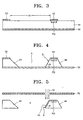
- FIGS. 3 through 5 illustrate the processing of the semiconductor substrate
- FIGS. 6 through 10 illustrate the forming of the units
- FIG. 11 illustrates the bonding
- FIG. 12 illustrates the mounting of the light emitting device.
- the light receiving device (PD) is installed at the semiconductor substrate 44.
- the semiconductor substrate 44 may be formed with the silicon substrate, which is sawed at a predetermined angle, for example, at a slope angle of 9.74 degrees.
- the light receiving device (PD) may be the photo diode.
- An etching stopper layer 50 is formed on the bottom surface of the semiconductor substrate 44.
- a mask layer 52 is formed to expose the predetermined region A1 of the semiconductor substrate 44 and cover a light receiving device (PD) on the top surface of the semiconductor substrate 44.
- the etching stopper layer 50 may be formed with a first insulating layer, for example, a Si 3 N 4 layer, and the mask layer 52 may be formed with a second insulating layer, for example, a Si 3 N 4 layer. As described above, the etching stopper layer 50 and the mask layer 52 may be formed with the same insulating layer, but it does not matter that they are formed with different insulating layers.
- the exposed portion of the semiconductor substrate 44 is etched.
- the etching may be performed until the etching stopper layer 50 is exposed.
- a through-hole (h) is provided in the semiconductor substrate 44 to expose the etching stopper layer 50 as shown in FIG. 4.
- a reflection unit 45 is installed on the inner surface (S) of the through-hole (h), which is provided in the semiconductor substrate 44, to reflect the laser beam in an upright direction.
- the semiconductor substrate 44 may be etched to have the inner surface of the through-hole (h) that is sloped at the predetermined angle ⁇ , for example, at the 45 degrees.
- the etching may be a wet etching.
- etchant with a high selectivity for silicon (Si) for example, kalium hydroxide (KOH) solution, may be used.
- the etching stopper layer 50 and the mask layer 52 are removed from the semiconductor substrate 44 through clean and dry processes.
- a shadow mask 70 is aligned at a position spaced apart from the semiconductor substrate 44 not having the etching stopper layer 50 and the mask layer 52 upward.
- the shadow mask 70 is designed to expose only a part of the inner surface of the through-hole (h), which is provided in the semiconductor substrate 44.
- Material 72 with high reflectance for example, aluminum (Al) is deposited on the semiconductor substrate 44 using the shadow mask 70. Since the remaining portion of the semiconductor substrate 44 excepting for the inner surface S of the through-hole h is shadowed by the shadow mask 70, the material 70 with the high reflectance is deposited only on the inner surface (S) of the through-hole (h), which is provided in the semiconductor substrate 44, to have a uniform thickness.
- the reflection unit 45 is formed on the inner surface (S) of the through-hole h, which is provided in the semiconductor substrate 44.
- the reflection unit 45 reflects the laser beam in the upright direction.
- the shadow mask 70 is removed. Since the reflection unit 45 is to receive and reflects the laser beam emitted from the light emitting device to be installed in a subsequent process, it is preferable that the reflection unit 45 may be disposed to be at the same height as that of the laser beam emission surface of the light emitting device.
- a conductive layer 42 is formed on the glass substrate 40.
- An adhesive layer and a main wire layer may be sequentially layered to form the conductive layer 42.
- the adhesive layer may be formed with a chromium (Cr) layer
- the main wire layer may be formed with a gold (Au) layer.
- the conductive layer 42 may be dual-layered, but may be also single-layered in case where the conductive layer 42 has the large adhesive force with the glass substrate 40 and the excellent conductivity.
- a mold layer 80 is formed on the glass substrate 40 to cover the conductive layer 42. After that, a through-hole 82 is formed in the mold layer 80 to form the flip-chip bonding unit.
- the mold layer 80 may be a photoresist layer, for example.
- the through-hole 82 of the mold layer 80 is filled with a flip-chip bonding unit 46.
- the flip-chip bonding unit 46 may be a solder bump, for example, which is formed by sequentially layering a gold layer and a tin layer.
- the flip-chip bonding unit 46 may be formed using an electroplating, but may be also formed using different methods.
- the flip-chip bonding unit 46 may be single-layered. In this case, the flip-chip bonding unit 46 may be formed using the electroplating or using the different methods.
- the mold layer 80 is ashed and stripped for removal to complete the flip-chip bonding unit 46 on the conductive layer 42 as shown in FIG. 9.
- a photosensitive pattern (not shown) is formed to define the flip-chip bonding unit 46 and a portion around the flip-chip bonding unit 46 of the conductive layer 42, and expose the remaining portion of the conductive layer 42.
- the exposed portion of the conductive layer 42 is removed using the photosensitive pattern as an etching mask. After that, the photosensitive pattern is removed.
- a conductive layer pattern on which the flip-chip bonding unit 46 is formed that is, an electrode wire 42a is formed on the glass substrate 40. Additionally, a portion of the glass substrate 40 is exposed.
- the bonding process is performed.
- the semiconductor substrate 44 in which the through-hole h is formed and where the reflection unit 45 is installed on the surface S sloped at 45 degrees of the through-hole h is aligned over the glass substrate 40.
- the semiconductor substrate 44 may preferably be aligned such that the flip-chip bonding unit 46 is disposed within the through-hole (h) of the semiconductor substrate 44, and a portion of the semiconductor substrate 44 on which the light receiving device (PD) is installed is disposed over the electrode wire 42a, and the reflection unit 43 faces with the flip-chip bonding unit 46.
- the above-aligned semiconductor substrate 44 puts down as it stands, and is anodic-bonded in contact with the glass substrate 40 and the electrode wire 42a.
- the light emitting device 48 for example, the laser diode is installed on the electrode wire 42a using the flip-chip bonding unit 46.
- the inventive micro optical bench structure and method of manufacturing the same a photolithography having high difficulty is not required in a cavity structure having a large step coverage, and a drawback can be avoided in which the step coverage of the photoresist layer is degraded at the edge of the slope surface, and a manufacture process can be simplified because a developing process for a structure with a deep step coverage does not require.
- the present invention can enhance the reproducibility and reliability and can reduce a production cost while can increase yield and productivity. Further, since the present invention can be omitt the conventional high difficulty processes, a process sequence can be reduced below current 50%.
- the conductive layer 42 can be patterned to form the electrode wire 42a.
- the light receiving device (PD) can be installed on the semiconductor substrate 44, which is in contact with the glass substrate 40, not the electrode wire 42a.
- the installing of the light emitting device can be performed earlier than the bonding. That is, before the semiconductor substrate 44 and the glass substrate 40 are bonded to each other, the light emitting device 48 can be installed on the flip-chip bonding unit 46.
- the light receiving device (PD) can be installed before or after the mounting of the light emitting device 48.
- the reflection unit 45 can be installed after the bonding.
- the semiconductor substrate 42a and the glass substrate 40 are bonded to each other and then, the reflection unit 45 can be installed on the slope surface (S) of the through-hole (h) before or after the installing of the light emitting unit 48 on the flip-chip bonding unit 46.
Landscapes
- Physics & Mathematics (AREA)
- Optics & Photonics (AREA)
- Condensed Matter Physics & Semiconductors (AREA)
- Electromagnetism (AREA)
- General Physics & Mathematics (AREA)
- Life Sciences & Earth Sciences (AREA)
- Forests & Forestry (AREA)
- Wood Science & Technology (AREA)
- Engineering & Computer Science (AREA)
- Led Device Packages (AREA)
- Micromachines (AREA)
- Investigating Or Analysing Materials By Optical Means (AREA)
- Semiconductor Lasers (AREA)
Applications Claiming Priority (2)
| Application Number | Priority Date | Filing Date | Title |
|---|---|---|---|
| KR2004002251 | 2004-01-13 | ||
| KR1020040002251A KR100906475B1 (ko) | 2004-01-13 | 2004-01-13 | 마이크로 광학벤치 구조물 및 그 제조방법 |
Publications (2)
| Publication Number | Publication Date |
|---|---|
| EP1555665A2 true EP1555665A2 (fr) | 2005-07-20 |
| EP1555665A3 EP1555665A3 (fr) | 2006-12-27 |
Family
ID=34617446
Family Applications (1)
| Application Number | Title | Priority Date | Filing Date |
|---|---|---|---|
| EP05000585A Withdrawn EP1555665A3 (fr) | 2004-01-13 | 2005-01-13 | Structure de banc micro optique et méthode pour sa fabrication |
Country Status (4)
| Country | Link |
|---|---|
| US (1) | US7456434B2 (fr) |
| EP (1) | EP1555665A3 (fr) |
| JP (1) | JP2005203782A (fr) |
| KR (1) | KR100906475B1 (fr) |
Cited By (1)
| Publication number | Priority date | Publication date | Assignee | Title |
|---|---|---|---|---|
| EP1988577B1 (fr) * | 2007-04-30 | 2017-04-05 | Tridonic Jennersdorf GmbH | Module à diode électroluminescente avec plateforme de silicium |
Families Citing this family (15)
| Publication number | Priority date | Publication date | Assignee | Title |
|---|---|---|---|---|
| JP4981342B2 (ja) * | 2006-04-04 | 2012-07-18 | 日立協和エンジニアリング株式会社 | サブマウントおよびその製造方法 |
| KR101131782B1 (ko) | 2011-07-19 | 2012-03-30 | 디지털옵틱스 코포레이션 이스트 | 집적 모듈용 기판 |
| US9064773B2 (en) * | 2012-10-26 | 2015-06-23 | Lg Innotek Co., Ltd. | Light emitting device package |
| US12402466B2 (en) | 2015-01-23 | 2025-08-26 | Vuereal Inc. | Micro device integration into system substrate |
| WO2016116889A1 (fr) | 2015-01-23 | 2016-07-28 | Gholamreza Chaji | Transfert sélectif de micro-dispositif vers un substrat récepteur |
| US10134803B2 (en) | 2015-01-23 | 2018-11-20 | Vuereal Inc. | Micro device integration into system substrate |
| US10700120B2 (en) * | 2015-01-23 | 2020-06-30 | Vuereal Inc. | Micro device integration into system substrate |
| JP6217706B2 (ja) | 2015-07-29 | 2017-10-25 | 日亜化学工業株式会社 | 光学部材の製造方法、半導体レーザ装置の製造方法及び半導体レーザ装置 |
| JP6354704B2 (ja) | 2015-08-25 | 2018-07-11 | 日亜化学工業株式会社 | 光学部材の製造方法、半導体レーザ装置の製造方法及び半導体レーザ装置 |
| US20170215280A1 (en) | 2016-01-21 | 2017-07-27 | Vuereal Inc. | Selective transfer of micro devices |
| JP6631502B2 (ja) | 2016-12-27 | 2020-01-15 | 日亜化学工業株式会社 | レーザパッケージの製造方法 |
| US10209477B1 (en) * | 2017-05-25 | 2019-02-19 | Lockheed Martin Coherent Technologies, Inc. | Systems and methods for reconfigurable micro-optic assemblies |
| JP7332860B2 (ja) * | 2019-05-29 | 2023-08-24 | 日亜化学工業株式会社 | 発光装置 |
| DE102019115597A1 (de) * | 2019-06-07 | 2020-12-10 | OSRAM Opto Semiconductors Gesellschaft mit beschränkter Haftung | Halbleiterlaservorrichtung und optoelektronisches Strahlumlenkelement für eine Halbleiterlaservorrichtung |
| JP7289744B2 (ja) * | 2019-07-11 | 2023-06-12 | 株式会社ジャパンディスプレイ | 表示装置、及びその製造方法 |
Family Cites Families (22)
| Publication number | Priority date | Publication date | Assignee | Title |
|---|---|---|---|---|
| JPS62298194A (ja) * | 1986-06-18 | 1987-12-25 | Fujitsu Ltd | レ−ザ発光装置 |
| JP2892820B2 (ja) * | 1990-11-26 | 1999-05-17 | 松下電子工業株式会社 | 半導体レーザ装置 |
| DE59305898D1 (de) * | 1993-12-22 | 1997-04-24 | Siemens Ag | Optoelektronisches Bauelement und Verfahren zu dessen Herstellung |
| JPH09191154A (ja) * | 1996-01-10 | 1997-07-22 | Mitsubishi Electric Corp | 半導体レーザ装置 |
| JP3430827B2 (ja) * | 1996-11-12 | 2003-07-28 | 横河電機株式会社 | 半導体デバイスの製造方法 |
| JPH1166590A (ja) * | 1997-08-15 | 1999-03-09 | Toshiba Corp | 光集積ユニット、光ピックアップ装置およびdvdシステム |
| US6137121A (en) * | 1997-10-01 | 2000-10-24 | Mitsubishi Denki Kabushiki Kaisha | Integrated semiconductor light generating and detecting device |
| JPH11186614A (ja) * | 1997-12-22 | 1999-07-09 | Rohm Co Ltd | チップ型led |
| JPH11233875A (ja) * | 1998-02-12 | 1999-08-27 | Toshiba Corp | 半導体レーザ装置 |
| JP2000049414A (ja) * | 1998-07-27 | 2000-02-18 | Canon Inc | 光機能素子装置、これを用いた光送受信装置、光インターコネクション装置および光記録装置 |
| US6271049B1 (en) | 1998-09-14 | 2001-08-07 | Siemens Aktiengesellschaft | Method for producing an optoelectronic component |
| JP2001014717A (ja) | 1999-04-28 | 2001-01-19 | Matsushita Electronics Industry Corp | 光学装置 |
| JP4582489B2 (ja) | 2000-01-21 | 2010-11-17 | 住友電気工業株式会社 | 発光装置 |
| JP3735528B2 (ja) | 2000-10-31 | 2006-01-18 | 株式会社東芝 | 半導体レーザ装置 |
| JP2002169064A (ja) * | 2000-11-30 | 2002-06-14 | Kyocera Corp | 光部品実装用基板及びその製造方法並びに光モジュール |
| KR100456984B1 (ko) * | 2001-03-06 | 2004-11-10 | 가부시끼가이샤 도시바 | 반도체 레이저 장치 |
| US6687272B2 (en) * | 2001-09-18 | 2004-02-03 | Kabushiki Kaisha Toshiba | Semiconductor laser device |
| JP4122784B2 (ja) * | 2001-09-19 | 2008-07-23 | 松下電工株式会社 | 発光装置 |
| JP2003229627A (ja) * | 2002-02-01 | 2003-08-15 | Hitachi Ltd | 光デバイスの実装方法及び光ヘッド装置 |
| JP4036658B2 (ja) * | 2002-02-25 | 2008-01-23 | シャープ株式会社 | 窒化物系化合物半導体レーザ装置およびその製造方法 |
| JP2003302261A (ja) * | 2002-04-05 | 2003-10-24 | Yazaki Corp | 指針式指示装置 |
| KR100492534B1 (ko) * | 2002-11-29 | 2005-06-02 | 엘지전자 주식회사 | 광 발생기 모듈, 광 검출기 모듈, 그들을 결합한 광픽업장치 및 그들의 제조방법 |
-
2004
- 2004-01-13 KR KR1020040002251A patent/KR100906475B1/ko not_active Expired - Fee Related
-
2005
- 2005-01-12 JP JP2005004671A patent/JP2005203782A/ja active Pending
- 2005-01-13 US US11/033,720 patent/US7456434B2/en not_active Expired - Fee Related
- 2005-01-13 EP EP05000585A patent/EP1555665A3/fr not_active Withdrawn
Cited By (1)
| Publication number | Priority date | Publication date | Assignee | Title |
|---|---|---|---|---|
| EP1988577B1 (fr) * | 2007-04-30 | 2017-04-05 | Tridonic Jennersdorf GmbH | Module à diode électroluminescente avec plateforme de silicium |
Also Published As
| Publication number | Publication date |
|---|---|
| JP2005203782A (ja) | 2005-07-28 |
| EP1555665A3 (fr) | 2006-12-27 |
| KR20050074042A (ko) | 2005-07-18 |
| US7456434B2 (en) | 2008-11-25 |
| US20050169570A1 (en) | 2005-08-04 |
| KR100906475B1 (ko) | 2009-07-08 |
Similar Documents
| Publication | Publication Date | Title |
|---|---|---|
| EP1555665A2 (fr) | Structure de banc micro optique et méthode pour sa fabrication | |
| JP4416731B2 (ja) | 発光ダイオードパッケージ及びその製造方法 | |
| KR100588705B1 (ko) | 반도체 레이저 장치 및 그 제조 방법 | |
| US6640021B2 (en) | Fabrication of a hybrid integrated circuit device including an optoelectronic chip | |
| US7196357B2 (en) | Optical semiconductor apparatus | |
| CN115248477B (zh) | 封装件及其形成方法 | |
| US20020008325A1 (en) | Functional device unit and method of producing the same | |
| CN103257398A (zh) | 制造聚合物波导的方法 | |
| KR20080100767A (ko) | 광전기 혼재 기판 | |
| US20210159142A1 (en) | Manufacturing method of chip package structure | |
| JP2002033410A (ja) | 機能デバイスユニット及びその製造方法 | |
| JP3440679B2 (ja) | 半導体装置 | |
| US20210096298A1 (en) | Optical waveguide circuit substrate and manufacturing method thereof | |
| KR100590534B1 (ko) | 마이크로 광학벤치 구조물 및 그 제조방법 | |
| WO2004068665A2 (fr) | Technique d'emballage a l'echelle de la tranche pour emballer hermetiquement des elements optiques et emballages hermetiques correspondants | |
| JPH0582810A (ja) | 光電変換装置 | |
| JP5431232B2 (ja) | 半導体装置 | |
| JPH04217375A (ja) | 半導体装置とその作製方法 | |
| JPH071794B2 (ja) | ハイブリッド光ic装置およびその製造方法 | |
| JP4122649B2 (ja) | Siキャリアの製造方法 | |
| KR100601940B1 (ko) | 마이크로 광픽업 및 그 제조방법 | |
| KR100282395B1 (ko) | 미소가동거울의 제조방법 | |
| KR100429515B1 (ko) | 버섯형상의 도금층을 구비한 광통신 소자 제작 방법 | |
| JP4671480B2 (ja) | 光実装基板の製造方法及び光モジュールの製造方法 | |
| JP4841110B2 (ja) | 光電子混在基板 |
Legal Events
| Date | Code | Title | Description |
|---|---|---|---|
| PUAI | Public reference made under article 153(3) epc to a published international application that has entered the european phase |
Free format text: ORIGINAL CODE: 0009012 |
|
| 17P | Request for examination filed |
Effective date: 20050113 |
|
| AK | Designated contracting states |
Kind code of ref document: A2 Designated state(s): AT BE BG CH CY CZ DE DK EE ES FI FR GB GR HU IE IS IT LI LT LU MC NL PL PT RO SE SI SK TR |
|
| AX | Request for extension of the european patent |
Extension state: AL BA HR LV MK YU |
|
| RIN1 | Information on inventor provided before grant (corrected) |
Inventor name: HWANG, WOONG-LIN Inventor name: CHOI, HYUNG Inventor name: YOU, JAE-HO Inventor name: CHUNG, SEOK-WHAN Inventor name: KIM, YONG-SUNG |
|
| PUAL | Search report despatched |
Free format text: ORIGINAL CODE: 0009013 |
|
| AK | Designated contracting states |
Kind code of ref document: A3 Designated state(s): AT BE BG CH CY CZ DE DK EE ES FI FR GB GR HU IE IS IT LI LT LU MC NL PL PT RO SE SI SK TR |
|
| AX | Request for extension of the european patent |
Extension state: AL BA HR LV MK YU |
|
| AKX | Designation fees paid |
Designated state(s): DE FR GB |
|
| 17Q | First examination report despatched |
Effective date: 20071102 |
|
| RAP1 | Party data changed (applicant data changed or rights of an application transferred) |
Owner name: SAMSUNG ELECTRONICS CO., LTD. |
|
| STAA | Information on the status of an ep patent application or granted ep patent |
Free format text: STATUS: THE APPLICATION IS DEEMED TO BE WITHDRAWN |
|
| 18D | Application deemed to be withdrawn |
Effective date: 20130801 |