EP1548845A1 - Verfahren zur Behandlung von Pulverkörner - Google Patents
Verfahren zur Behandlung von Pulverkörner Download PDFInfo
- Publication number
- EP1548845A1 EP1548845A1 EP03029577A EP03029577A EP1548845A1 EP 1548845 A1 EP1548845 A1 EP 1548845A1 EP 03029577 A EP03029577 A EP 03029577A EP 03029577 A EP03029577 A EP 03029577A EP 1548845 A1 EP1548845 A1 EP 1548845A1
- Authority
- EP
- European Patent Office
- Prior art keywords
- grains
- powder
- sulfur
- temperature
- powder grains
- Prior art date
- Legal status (The legal status is an assumption and is not a legal conclusion. Google has not performed a legal analysis and makes no representation as to the accuracy of the status listed.)
- Granted
Links
- 239000000843 powder Substances 0.000 title claims abstract description 107
- 238000000034 method Methods 0.000 title claims abstract description 47
- 230000008569 process Effects 0.000 title claims abstract description 13
- 239000002245 particle Substances 0.000 title description 11
- NINIDFKCEFEMDL-UHFFFAOYSA-N Sulfur Chemical compound [S] NINIDFKCEFEMDL-UHFFFAOYSA-N 0.000 claims abstract description 42
- 229910052717 sulfur Inorganic materials 0.000 claims abstract description 37
- 239000011593 sulfur Substances 0.000 claims abstract description 36
- 229910052738 indium Inorganic materials 0.000 claims abstract description 31
- 229910052733 gallium Inorganic materials 0.000 claims abstract description 29
- 239000012528 membrane Substances 0.000 claims abstract description 10
- 239000004065 semiconductor Substances 0.000 claims abstract description 6
- 239000003708 ampul Substances 0.000 claims description 24
- 150000001875 compounds Chemical class 0.000 claims description 19
- 239000000203 mixture Substances 0.000 claims description 19
- -1 Se2 compound Chemical class 0.000 abstract 1
- 239000011669 selenium Substances 0.000 description 33
- 239000012071 phase Substances 0.000 description 16
- 230000004907 flux Effects 0.000 description 11
- 239000000126 substance Substances 0.000 description 8
- 229910052802 copper Inorganic materials 0.000 description 7
- 239000000155 melt Substances 0.000 description 7
- 238000004519 manufacturing process Methods 0.000 description 6
- 239000000956 alloy Substances 0.000 description 5
- 229910045601 alloy Inorganic materials 0.000 description 5
- 239000007788 liquid Substances 0.000 description 5
- 238000005259 measurement Methods 0.000 description 5
- 238000005987 sulfurization reaction Methods 0.000 description 5
- 238000006243 chemical reaction Methods 0.000 description 4
- 238000009826 distribution Methods 0.000 description 4
- 238000010438 heat treatment Methods 0.000 description 4
- VYPSYNLAJGMNEJ-UHFFFAOYSA-N Silicium dioxide Chemical compound O=[Si]=O VYPSYNLAJGMNEJ-UHFFFAOYSA-N 0.000 description 3
- 230000006872 improvement Effects 0.000 description 3
- 229910052711 selenium Inorganic materials 0.000 description 3
- BUGBHKTXTAQXES-UHFFFAOYSA-N Selenium Chemical compound [Se] BUGBHKTXTAQXES-UHFFFAOYSA-N 0.000 description 2
- 230000008901 benefit Effects 0.000 description 2
- 230000008859 change Effects 0.000 description 2
- 230000007423 decrease Effects 0.000 description 2
- 238000000635 electron micrograph Methods 0.000 description 2
- 239000000463 material Substances 0.000 description 2
- 229920005597 polymer membrane Polymers 0.000 description 2
- 238000002360 preparation method Methods 0.000 description 2
- 229910000838 Al alloy Inorganic materials 0.000 description 1
- 239000000853 adhesive Substances 0.000 description 1
- 230000001070 adhesive effect Effects 0.000 description 1
- 238000000137 annealing Methods 0.000 description 1
- 238000001816 cooling Methods 0.000 description 1
- 239000013078 crystal Substances 0.000 description 1
- 238000010586 diagram Methods 0.000 description 1
- 230000000694 effects Effects 0.000 description 1
- 230000037406 food intake Effects 0.000 description 1
- 239000011521 glass Substances 0.000 description 1
- 238000011835 investigation Methods 0.000 description 1
- 239000007791 liquid phase Substances 0.000 description 1
- 238000000879 optical micrograph Methods 0.000 description 1
- 238000010791 quenching Methods 0.000 description 1
- 230000000171 quenching effect Effects 0.000 description 1
- 238000001953 recrystallisation Methods 0.000 description 1
- 230000003716 rejuvenation Effects 0.000 description 1
- 238000005204 segregation Methods 0.000 description 1
- 238000010583 slow cooling Methods 0.000 description 1
- 239000007790 solid phase Substances 0.000 description 1
- 239000007858 starting material Substances 0.000 description 1
- 239000000758 substrate Substances 0.000 description 1
- 230000002123 temporal effect Effects 0.000 description 1
- 239000006163 transport media Substances 0.000 description 1
- XLYOFNOQVPJJNP-UHFFFAOYSA-N water Substances O XLYOFNOQVPJJNP-UHFFFAOYSA-N 0.000 description 1
Images


Classifications
-
- C—CHEMISTRY; METALLURGY
- C01—INORGANIC CHEMISTRY
- C01B—NON-METALLIC ELEMENTS; COMPOUNDS THEREOF; METALLOIDS OR COMPOUNDS THEREOF NOT COVERED BY SUBCLASS C01C
- C01B19/00—Selenium; Tellurium; Compounds thereof
-
- H—ELECTRICITY
- H10—SEMICONDUCTOR DEVICES; ELECTRIC SOLID-STATE DEVICES NOT OTHERWISE PROVIDED FOR
- H10F—INORGANIC SEMICONDUCTOR DEVICES SENSITIVE TO INFRARED RADIATION, LIGHT, ELECTROMAGNETIC RADIATION OF SHORTER WAVELENGTH OR CORPUSCULAR RADIATION
- H10F77/00—Constructional details of devices covered by this subclass
- H10F77/10—Semiconductor bodies
- H10F77/12—Active materials
- H10F77/126—Active materials comprising only Group I-III-VI chalcopyrite materials, e.g. CuInSe2, CuGaSe2 or CuInGaSe2 [CIGS]
-
- H—ELECTRICITY
- H10—SEMICONDUCTOR DEVICES; ELECTRIC SOLID-STATE DEVICES NOT OTHERWISE PROVIDED FOR
- H10F—INORGANIC SEMICONDUCTOR DEVICES SENSITIVE TO INFRARED RADIATION, LIGHT, ELECTROMAGNETIC RADIATION OF SHORTER WAVELENGTH OR CORPUSCULAR RADIATION
- H10F10/00—Individual photovoltaic cells, e.g. solar cells
-
- H—ELECTRICITY
- H10—SEMICONDUCTOR DEVICES; ELECTRIC SOLID-STATE DEVICES NOT OTHERWISE PROVIDED FOR
- H10F—INORGANIC SEMICONDUCTOR DEVICES SENSITIVE TO INFRARED RADIATION, LIGHT, ELECTROMAGNETIC RADIATION OF SHORTER WAVELENGTH OR CORPUSCULAR RADIATION
- H10F71/00—Manufacture or treatment of devices covered by this subclass
-
- Y—GENERAL TAGGING OF NEW TECHNOLOGICAL DEVELOPMENTS; GENERAL TAGGING OF CROSS-SECTIONAL TECHNOLOGIES SPANNING OVER SEVERAL SECTIONS OF THE IPC; TECHNICAL SUBJECTS COVERED BY FORMER USPC CROSS-REFERENCE ART COLLECTIONS [XRACs] AND DIGESTS
- Y02—TECHNOLOGIES OR APPLICATIONS FOR MITIGATION OR ADAPTATION AGAINST CLIMATE CHANGE
- Y02E—REDUCTION OF GREENHOUSE GAS [GHG] EMISSIONS, RELATED TO ENERGY GENERATION, TRANSMISSION OR DISTRIBUTION
- Y02E10/00—Energy generation through renewable energy sources
- Y02E10/50—Photovoltaic [PV] energy
- Y02E10/541—CuInSe2 material PV cells
-
- Y—GENERAL TAGGING OF NEW TECHNOLOGICAL DEVELOPMENTS; GENERAL TAGGING OF CROSS-SECTIONAL TECHNOLOGIES SPANNING OVER SEVERAL SECTIONS OF THE IPC; TECHNICAL SUBJECTS COVERED BY FORMER USPC CROSS-REFERENCE ART COLLECTIONS [XRACs] AND DIGESTS
- Y02—TECHNOLOGIES OR APPLICATIONS FOR MITIGATION OR ADAPTATION AGAINST CLIMATE CHANGE
- Y02P—CLIMATE CHANGE MITIGATION TECHNOLOGIES IN THE PRODUCTION OR PROCESSING OF GOODS
- Y02P70/00—Climate change mitigation technologies in the production process for final industrial or consumer products
- Y02P70/50—Manufacturing or production processes characterised by the final manufactured product
Definitions
- the sulfur is preferably at a temperature of about Heated to 100 ° C.
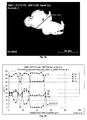
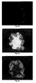
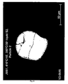
- FIG. 5c shows the result of an S content sensitive backscatter electron uptake of the ingestion in of the powder particle shown in FIG. 5a.
- the bright areas in 5c correspond to regions with a high S content, the dark areas correspond to places with one low S content.
Landscapes
- Chemical & Material Sciences (AREA)
- Organic Chemistry (AREA)
- Inorganic Chemistry (AREA)
- Photovoltaic Devices (AREA)
- Glanulating (AREA)
- Cereal-Derived Products (AREA)
- Nonmetallic Welding Materials (AREA)
- Seeds, Soups, And Other Foods (AREA)
- Manufacture And Refinement Of Metals (AREA)
- Physical Or Chemical Processes And Apparatus (AREA)
Abstract
Description
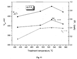
Besonders gute Ergebnisse im Hinblick auf die photovoltaischen Eigenschaften der Körner konnten dabei durch eine 5-minütige Behandlung bei 410°C und eine anschließende 30-minütige Behandlung bei 380°C erzielt werden.
Claims (9)
- Verfahren zur Behandlung von aus einer Cu(In,Ga)Se2-Verbindung bestehenden Pulverkörnern,
dadurch gekennzeichnet, dass die Pulverkörner und eine Menge Schwefel in ein Gefäß hineingegeben werden und der aus den Körnern und dem Schwefel bestehende Inhalt des Gefäßes erhitzt wird und über einen Zeitraum auf einer konstanten Temperatur gehalten wird. - Verfahren nach Anspruch 1, dadurch gekennzeichnet, dass die Körner und Schwefel in eine Zwei-Zonen-Ampulle gefüllt werden, wobei die Körner in eine der Zonen und die Menge Schwefel in die andere Zone hineingegeben werden.
- Verfahren nach einem oder beiden der Ansprüche 1 und 2,
dadurch gekennzeichnet, dass die Körner auf eine Temperatur zwischen 400°C und 600°C erhitzt werden. - Verfahren nach einem oder mehreren der vorangegangenen Ansprüche,
dadurch gekennzeichnet, dass der Schwefel auf eine Temperatur von etwa 100°C erhitzt wird. - Verfahren nach einem oder mehreren der vorangegangenen Ansprüche,
dadurch gekennzeichnet, dass die Körner und der Schwefel über einen Zeitraum zwischen einer Stunde und 50 Stunden jeweils auf einer konstanten Temperatur gehalten werden. - Verfahren nach Anspruch 1, dadurch gekennzeichnet, dass ein aus den Pulverkörnern und dem Schwefel bestehendes Gemisch in eine Ampulle gefüllt wird.
- Verfahren nach einem oder beiden der Ansprüche 1 und 6,
dadurch gekennzeichnet, dass das aus den Pulverkörnern und dem Schwefel bestehende Gemisch auf eine Temperatur zwischen 300°C und 600°C erhitzt wird. - Verfahren nach einem oder mehreren der Ansprüche 1, 6 und 7,
dadurch gekennzeichnet, dass das Gemisch aus Pulverkörnern und Schwefel über einen Zeitraum zwischen 5 Minuten und 4 Stunden auf einer Temperatur gehalten wird. - Monokornmembran-Solarzelle, beinhaltend einen Rückkontakt, eine Monokornmembran, mindestes eine Halbleiterschicht und einen Frontkontakt,
dadurch gekennzeichnet, dass die Monokornmembran mit einem Verfahren nach einem oder mehreren der Ansprüche 1 bis 8 behandelte Pulverkörner enthält.
Priority Applications (15)
| Application Number | Priority Date | Filing Date | Title |
|---|---|---|---|
| SI200330667T SI1548845T1 (sl) | 2003-12-22 | 2003-12-22 | postopek za obdelavo prašnih zrn |
| DK03029577T DK1548845T3 (da) | 2003-12-22 | 2003-12-22 | Fremgangsmåde til behandling af pulverkorn |
| AT03029577T ATE348408T1 (de) | 2003-12-22 | 2003-12-22 | Verfahren zur behandlung von pulverkörner |
| PT03029577T PT1548845E (pt) | 2003-12-22 | 2003-12-22 | Processo para tratar partículas de pó |
| DE50305977T DE50305977D1 (de) | 2003-12-22 | 2003-12-22 | Verfahren zur Behandlung von Pulverkörner |
| EP03029577A EP1548845B1 (de) | 2003-12-22 | 2003-12-22 | Verfahren zur Behandlung von Pulverkörner |
| ES03029577T ES2279057T3 (es) | 2003-12-22 | 2003-12-22 | Procedimiento para tratar granos de polvo. |
| JP2006544314A JP2007515371A (ja) | 2003-12-22 | 2004-12-14 | 粉体の処理方法 |
| PL04803855T PL1704599T3 (pl) | 2003-12-22 | 2004-12-14 | Metoda obróbki ziaren proszku |
| CNB200480036244XA CN100461460C (zh) | 2003-12-22 | 2004-12-14 | 处理粉末颗粒的方法 |
| CA002547352A CA2547352A1 (en) | 2003-12-22 | 2004-12-14 | Method for treating powder particles |
| PCT/EP2004/014232 WO2005064691A1 (de) | 2003-12-22 | 2004-12-14 | Verfahren zur behandlung von pulverkörnern |
| KR1020067014667A KR100851043B1 (ko) | 2003-12-22 | 2004-12-14 | 분말 입자의 처리 방법 |
| US10/582,571 US20070113888A1 (en) | 2003-12-22 | 2004-12-14 | Method for treating powder particles |
| EP04803855A EP1704599B1 (de) | 2003-12-22 | 2004-12-14 | Verfahren zur behandlung von pulverkörnern |
Applications Claiming Priority (1)
| Application Number | Priority Date | Filing Date | Title |
|---|---|---|---|
| EP03029577A EP1548845B1 (de) | 2003-12-22 | 2003-12-22 | Verfahren zur Behandlung von Pulverkörner |
Publications (2)
| Publication Number | Publication Date |
|---|---|
| EP1548845A1 true EP1548845A1 (de) | 2005-06-29 |
| EP1548845B1 EP1548845B1 (de) | 2006-12-13 |
Family
ID=34530696
Family Applications (2)
| Application Number | Title | Priority Date | Filing Date |
|---|---|---|---|
| EP03029577A Expired - Lifetime EP1548845B1 (de) | 2003-12-22 | 2003-12-22 | Verfahren zur Behandlung von Pulverkörner |
| EP04803855A Expired - Lifetime EP1704599B1 (de) | 2003-12-22 | 2004-12-14 | Verfahren zur behandlung von pulverkörnern |
Family Applications After (1)
| Application Number | Title | Priority Date | Filing Date |
|---|---|---|---|
| EP04803855A Expired - Lifetime EP1704599B1 (de) | 2003-12-22 | 2004-12-14 | Verfahren zur behandlung von pulverkörnern |
Country Status (14)
| Country | Link |
|---|---|
| US (1) | US20070113888A1 (de) |
| EP (2) | EP1548845B1 (de) |
| JP (1) | JP2007515371A (de) |
| KR (1) | KR100851043B1 (de) |
| CN (1) | CN100461460C (de) |
| AT (1) | ATE348408T1 (de) |
| CA (1) | CA2547352A1 (de) |
| DE (1) | DE50305977D1 (de) |
| DK (1) | DK1548845T3 (de) |
| ES (1) | ES2279057T3 (de) |
| PL (1) | PL1704599T3 (de) |
| PT (1) | PT1548845E (de) |
| SI (1) | SI1548845T1 (de) |
| WO (1) | WO2005064691A1 (de) |
Families Citing this family (1)
| Publication number | Priority date | Publication date | Assignee | Title |
|---|---|---|---|---|
| DE102008040147A1 (de) | 2008-07-03 | 2010-01-28 | Crystalsol Og | Verfahren zur Herstellung einer Monokornmembran für eine Solarzelle sowie Monokornmembran nebst Solarzelle |
Citations (1)
| Publication number | Priority date | Publication date | Assignee | Title |
|---|---|---|---|---|
| WO1994027328A1 (en) * | 1993-05-07 | 1994-11-24 | Siemens Solar Industries International, Inc. | Process for at least partially converting semi-conductor films of the i-iii-vi2-type |
Family Cites Families (13)
| Publication number | Priority date | Publication date | Assignee | Title |
|---|---|---|---|---|
| FR2071287A5 (de) * | 1969-12-23 | 1971-09-17 | Rhone Poulenc Sa | |
| US4335266A (en) * | 1980-12-31 | 1982-06-15 | The Boeing Company | Methods for forming thin-film heterojunction solar cells from I-III-VI.sub.2 |
| US4581108A (en) * | 1984-01-06 | 1986-04-08 | Atlantic Richfield Company | Process of forming a compound semiconductive material |
| JPS61263286A (ja) * | 1985-05-10 | 1986-11-21 | ハ−ン − マイトネル − インスチツ−ト・ベルリン・ゲゼルシャフト・ミット・ベシュレンクテル・ハフツング | CuInS2−半導体材料をベ−スとするホトアノ−ドを有する太陽電池及びその製法 |
| KR960003800B1 (ko) * | 1988-02-19 | 1996-03-22 | 가와사끼 세이데쓰 가부시끼가이샤 | 고순도 금속 규소의 제조방법 |
| JPH04326526A (ja) * | 1991-04-25 | 1992-11-16 | Dowa Mining Co Ltd | CuIn(Se1−xSx)2混晶薄膜の製造法 |
| US5356839A (en) * | 1993-04-12 | 1994-10-18 | Midwest Research Institute | Enhanced quality thin film Cu(In,Ga)Se2 for semiconductor device applications by vapor-phase recrystallization |
| JPH0789719A (ja) * | 1993-09-20 | 1995-04-04 | Hitachi Maxell Ltd | 銅インジウム硫化物またはセレン化物の製造法 |
| US5730852A (en) * | 1995-09-25 | 1998-03-24 | Davis, Joseph & Negley | Preparation of cuxinygazsen (X=0-2, Y=0-2, Z=0-2, N=0-3) precursor films by electrodeposition for fabricating high efficiency solar cells |
| JP3589380B2 (ja) * | 1997-06-05 | 2004-11-17 | 松下電器産業株式会社 | 半導体薄膜の製造方法および薄膜太陽電池の製造方法 |
| JP2001517493A (ja) * | 1997-09-26 | 2001-10-09 | ノーヴェン ファーマシューティカルズ インコーポレイテッド | 生体接着剤組成物及び活性薬剤の局所投与方法 |
| DE19828310C2 (de) * | 1998-06-25 | 2000-08-31 | Forschungszentrum Juelich Gmbh | Einkristallpulver- und Monokornmembranherstellung |
| US7019208B2 (en) * | 2001-11-20 | 2006-03-28 | Energy Photovoltaics | Method of junction formation for CIGS photovoltaic devices |
-
2003
- 2003-12-22 AT AT03029577T patent/ATE348408T1/de active
- 2003-12-22 DK DK03029577T patent/DK1548845T3/da active
- 2003-12-22 DE DE50305977T patent/DE50305977D1/de not_active Expired - Lifetime
- 2003-12-22 ES ES03029577T patent/ES2279057T3/es not_active Expired - Lifetime
- 2003-12-22 SI SI200330667T patent/SI1548845T1/sl unknown
- 2003-12-22 PT PT03029577T patent/PT1548845E/pt unknown
- 2003-12-22 EP EP03029577A patent/EP1548845B1/de not_active Expired - Lifetime
-
2004
- 2004-12-14 CN CNB200480036244XA patent/CN100461460C/zh not_active Expired - Fee Related
- 2004-12-14 KR KR1020067014667A patent/KR100851043B1/ko not_active Expired - Fee Related
- 2004-12-14 WO PCT/EP2004/014232 patent/WO2005064691A1/de not_active Ceased
- 2004-12-14 JP JP2006544314A patent/JP2007515371A/ja active Pending
- 2004-12-14 US US10/582,571 patent/US20070113888A1/en not_active Abandoned
- 2004-12-14 PL PL04803855T patent/PL1704599T3/pl unknown
- 2004-12-14 CA CA002547352A patent/CA2547352A1/en not_active Abandoned
- 2004-12-14 EP EP04803855A patent/EP1704599B1/de not_active Expired - Lifetime
Patent Citations (1)
| Publication number | Priority date | Publication date | Assignee | Title |
|---|---|---|---|---|
| WO1994027328A1 (en) * | 1993-05-07 | 1994-11-24 | Siemens Solar Industries International, Inc. | Process for at least partially converting semi-conductor films of the i-iii-vi2-type |
Non-Patent Citations (1)
| Title |
|---|
| ALTOSAAR M ET AL: "Monograin layer solar cells", PREPARATION AND CHARACTERIZATION, ELSEVIER SEQUOIA, NL, vol. 431-432, 1 May 2003 (2003-05-01), pages 466 - 469, XP004428688, ISSN: 0040-6090 * |
Also Published As
| Publication number | Publication date |
|---|---|
| KR20070015510A (ko) | 2007-02-05 |
| CN1890817A (zh) | 2007-01-03 |
| CA2547352A1 (en) | 2005-07-14 |
| JP2007515371A (ja) | 2007-06-14 |
| PT1548845E (pt) | 2007-03-30 |
| EP1704599B1 (de) | 2007-10-31 |
| ES2279057T3 (es) | 2007-08-16 |
| DE50305977D1 (de) | 2007-01-25 |
| DK1548845T3 (da) | 2008-05-19 |
| CN100461460C (zh) | 2009-02-11 |
| KR100851043B1 (ko) | 2008-08-12 |
| PL1704599T3 (pl) | 2008-03-31 |
| SI1548845T1 (sl) | 2007-06-30 |
| ATE348408T1 (de) | 2007-01-15 |
| EP1548845B1 (de) | 2006-12-13 |
| WO2005064691A1 (de) | 2005-07-14 |
| US20070113888A1 (en) | 2007-05-24 |
| EP1704599A1 (de) | 2006-09-27 |
Similar Documents
| Publication | Publication Date | Title |
|---|---|---|
| DE69304143T2 (de) | Methode zur Herstellung einer Zusammensetzung des Typs Chalkopyrit | |
| DE19630321C2 (de) | Verfahren zur Herstellung eines Kupfer-Indium-Schwefel-Selen-Dünnfilms und zur Herstellung eines Kupfer-Indium-Schwefel-Selen-Chalcopyrit-Kristalls | |
| DE19912961A1 (de) | Halbleiterdünnfilm, Herstellungsverfahren dafür, sowie den Halbleiterdünnfilm aufweisende Solarzelle | |
| DE10151415A1 (de) | Solarzelle | |
| EP1548159B1 (de) | Verfahren zur Herstellung von Cu(In,Ga)Se2 einkristallinem Pulver und Monokornmembran-Solarzelle enthaltend dieses Pulver | |
| DE2755500A1 (de) | Solarzelle und verfahren zu ihrer herstellung | |
| DE3011978A1 (de) | Szintillator und verfahren zu seiner herstellung | |
| EP1739210B1 (de) | Verfahren zur Herstellung von dotierten Halbleiter-Einkristallen, und III-V-Halbleiter-Einkristall | |
| DE2039381A1 (de) | Verfahren zur Herstellung einer Elektrolumineszenz-Vorrichtung und Vorrichtung dieser Art | |
| DE3336453A1 (de) | Verfahren zur oberflaechenbehandlung von ventilmetallen mit chalkogenen | |
| DE2736250A1 (de) | Halbleiterelemente und verfahren zu deren herstellung | |
| DE2529747C3 (de) | Verfahren zur Erzeugung von epitaktischen Aufwachsungen aus der flussigen Phase | |
| DE3882882T2 (de) | Verfahren zur Herstellung einer Siliziumstruktur auf einem Isolator. | |
| EP1548845B1 (de) | Verfahren zur Behandlung von Pulverkörner | |
| EP1060505B1 (de) | Verfahren zur herstellung eines mikroelektronischen halbleiterbauelements | |
| DE2158681B2 (de) | Verfahren zur Behandlung einer einen pn-Ubergang aufweisenden, lichtemittierenden Halbleitervorrichtung | |
| EP0136967B1 (de) | Photoelektrochemische Solarzelle und Verfahren zur Herstellung einer Arbeitselektrode für Solarzellen | |
| DE2923065A1 (de) | Elektrolumineszente und/oder lichterkennende dioden sowie verfahren zur herstellung dieser dioden | |
| DE3434552C2 (de) | ||
| DE102008024539B3 (de) | Strahlungswandler und dessen Verwendung insbesondere für die Röntgen-Computertomografie | |
| DE1719496B2 (de) | Verfahren zum Herstellen von kristallinen Verbindungshalbleiterschichten | |
| EP0227945A2 (de) | Verfahren zum Herstellen einer Solarzelle | |
| DE2830695C3 (de) | Vorrichtung zum Ziehen eines III/V-Verbindungseinkristalls aus einer Schmelze | |
| DE683330C (de) | Verfahren zur Herstellung von als lichtelektrisch empfindliches Organ bei Sperrschichtzellen dienenden Metallverbindungen | |
| DE102013209983A1 (de) | Verfahren zur Herstellung einer Dünnschichtsolarzelle und einer Verbindungshalbleiterschicht hierfür |
Legal Events
| Date | Code | Title | Description |
|---|---|---|---|
| PUAI | Public reference made under article 153(3) epc to a published international application that has entered the european phase |
Free format text: ORIGINAL CODE: 0009012 |
|
| AK | Designated contracting states |
Kind code of ref document: A1 Designated state(s): AT BE BG CH CY CZ DE DK EE ES FI FR GB GR HU IE IT LI LU MC NL PT RO SE SI SK TR |
|
| AX | Request for extension of the european patent |
Extension state: AL LT LV MK |
|
| 17P | Request for examination filed |
Effective date: 20051229 |
|
| AKX | Designation fees paid |
Designated state(s): AT BE BG CH CY CZ DE DK EE ES FI FR GB GR HU IE IT LI LU MC NL PT RO SE SI SK TR |
|
| GRAP | Despatch of communication of intention to grant a patent |
Free format text: ORIGINAL CODE: EPIDOSNIGR1 |
|
| GRAS | Grant fee paid |
Free format text: ORIGINAL CODE: EPIDOSNIGR3 |
|
| GRAA | (expected) grant |
Free format text: ORIGINAL CODE: 0009210 |
|
| AK | Designated contracting states |
Kind code of ref document: B1 Designated state(s): AT BE BG CH CY CZ DE DK EE ES FI FR GB GR HU IE IT LI LU MC NL PT RO SE SI SK TR |
|
| PG25 | Lapsed in a contracting state [announced via postgrant information from national office to epo] |
Ref country code: DK Free format text: LAPSE BECAUSE OF FAILURE TO SUBMIT A TRANSLATION OF THE DESCRIPTION OR TO PAY THE FEE WITHIN THE PRESCRIBED TIME-LIMIT Effective date: 20061213 |
|
| REG | Reference to a national code |
Ref country code: GB Ref legal event code: FG4D Free format text: NOT ENGLISH |
|
| REG | Reference to a national code |
Ref country code: CH Ref legal event code: EP |
|
| REG | Reference to a national code |
Ref country code: IE Ref legal event code: FG4D Free format text: LANGUAGE OF EP DOCUMENT: GERMAN |
|
| REF | Corresponds to: |
Ref document number: 50305977 Country of ref document: DE Date of ref document: 20070125 Kind code of ref document: P |
|
| REG | Reference to a national code |
Ref country code: RO Ref legal event code: EPE |
|
| GBT | Gb: translation of ep patent filed (gb section 77(6)(a)/1977) |
Effective date: 20070227 |
|
| REG | Reference to a national code |
Ref country code: PT Ref legal event code: SC4A Free format text: AVAILABILITY OF NATIONAL TRANSLATION Effective date: 20070313 |
|
| REG | Reference to a national code |
Ref country code: SE Ref legal event code: TRGR |
|
| REG | Reference to a national code |
Ref country code: CH Ref legal event code: NV Representative=s name: R. A. EGLI & CO. PATENTANWAELTE |
|
| REG | Reference to a national code |
Ref country code: GR Ref legal event code: EP Ref document number: 20070400743 Country of ref document: GR |
|
| REG | Reference to a national code |
Ref country code: EE Ref legal event code: FG4A Ref document number: E001126 Country of ref document: EE Effective date: 20070313 |
|
| ET | Fr: translation filed | ||
| REG | Reference to a national code |
Ref country code: HU Ref legal event code: AG4A Ref document number: E001658 Country of ref document: HU |
|
| REG | Reference to a national code |
Ref country code: ES Ref legal event code: FG2A Ref document number: 2279057 Country of ref document: ES Kind code of ref document: T3 |
|
| PLBE | No opposition filed within time limit |
Free format text: ORIGINAL CODE: 0009261 |
|
| STAA | Information on the status of an ep patent application or granted ep patent |
Free format text: STATUS: NO OPPOSITION FILED WITHIN TIME LIMIT |
|
| 26N | No opposition filed |
Effective date: 20070914 |
|
| REG | Reference to a national code |
Ref country code: DK Ref legal event code: EGE |
|
| REG | Reference to a national code |
Ref country code: DK Ref legal event code: T3 |
|
| PGFP | Annual fee paid to national office [announced via postgrant information from national office to epo] |
Ref country code: TR Payment date: 20071127 Year of fee payment: 5 |
|
| PGFP | Annual fee paid to national office [announced via postgrant information from national office to epo] |
Ref country code: CH Payment date: 20081215 Year of fee payment: 6 Ref country code: CZ Payment date: 20081216 Year of fee payment: 6 Ref country code: DK Payment date: 20081211 Year of fee payment: 6 Ref country code: IE Payment date: 20081229 Year of fee payment: 6 Ref country code: LU Payment date: 20081219 Year of fee payment: 6 Ref country code: MC Payment date: 20081212 Year of fee payment: 6 |
|
| PGFP | Annual fee paid to national office [announced via postgrant information from national office to epo] |
Ref country code: ES Payment date: 20081217 Year of fee payment: 6 Ref country code: PT Payment date: 20081203 Year of fee payment: 6 Ref country code: RO Payment date: 20081128 Year of fee payment: 6 Ref country code: SK Payment date: 20081219 Year of fee payment: 6 |
|
| PGFP | Annual fee paid to national office [announced via postgrant information from national office to epo] |
Ref country code: BG Payment date: 20081219 Year of fee payment: 6 Ref country code: IT Payment date: 20081222 Year of fee payment: 6 Ref country code: SE Payment date: 20081212 Year of fee payment: 6 |
|
| PGFP | Annual fee paid to national office [announced via postgrant information from national office to epo] |
Ref country code: GR Payment date: 20081218 Year of fee payment: 6 Ref country code: SI Payment date: 20081216 Year of fee payment: 6 |
|
| PGFP | Annual fee paid to national office [announced via postgrant information from national office to epo] |
Ref country code: CY Payment date: 20081205 Year of fee payment: 6 |
|
| PG25 | Lapsed in a contracting state [announced via postgrant information from national office to epo] |
Ref country code: TR Free format text: LAPSE BECAUSE OF NON-PAYMENT OF DUE FEES Effective date: 20061222 |
|
| PGFP | Annual fee paid to national office [announced via postgrant information from national office to epo] |
Ref country code: HU Payment date: 20081125 Year of fee payment: 6 |
|
| REG | Reference to a national code |
Ref country code: PT Ref legal event code: MM4A Free format text: LAPSE DUE TO NON-PAYMENT OF FEES Effective date: 20100622 |
|
| EUG | Se: european patent has lapsed | ||
| PG25 | Lapsed in a contracting state [announced via postgrant information from national office to epo] |
Ref country code: MC Free format text: LAPSE BECAUSE OF NON-PAYMENT OF DUE FEES Effective date: 20100701 Ref country code: PT Free format text: LAPSE BECAUSE OF NON-PAYMENT OF DUE FEES Effective date: 20100622 |
|
| REG | Reference to a national code |
Ref country code: CH Ref legal event code: PL |
|
| REG | Reference to a national code |
Ref country code: DK Ref legal event code: EBP |
|
| PG25 | Lapsed in a contracting state [announced via postgrant information from national office to epo] |
Ref country code: CZ Free format text: LAPSE BECAUSE OF NON-PAYMENT OF DUE FEES Effective date: 20091222 |
|
| REG | Reference to a national code |
Ref country code: SK Ref legal event code: MM4A Ref document number: E 1992 Country of ref document: SK Effective date: 20091222 |
|
| REG | Reference to a national code |
Ref country code: SI Ref legal event code: KO00 Effective date: 20100813 |
|
| PG25 | Lapsed in a contracting state [announced via postgrant information from national office to epo] |
Ref country code: CH Free format text: LAPSE BECAUSE OF NON-PAYMENT OF DUE FEES Effective date: 20091231 Ref country code: HU Free format text: LAPSE BECAUSE OF NON-PAYMENT OF DUE FEES Effective date: 20091223 Ref country code: IE Free format text: LAPSE BECAUSE OF NON-PAYMENT OF DUE FEES Effective date: 20091222 Ref country code: LI Free format text: LAPSE BECAUSE OF NON-PAYMENT OF DUE FEES Effective date: 20091231 |
|
| PG25 | Lapsed in a contracting state [announced via postgrant information from national office to epo] |
Ref country code: SI Free format text: LAPSE BECAUSE OF NON-PAYMENT OF DUE FEES Effective date: 20091223 Ref country code: SK Free format text: LAPSE BECAUSE OF NON-PAYMENT OF DUE FEES Effective date: 20091222 Ref country code: BG Free format text: LAPSE BECAUSE OF NON-PAYMENT OF DUE FEES Effective date: 20100630 |
|
| PG25 | Lapsed in a contracting state [announced via postgrant information from national office to epo] |
Ref country code: CY Free format text: LAPSE BECAUSE OF FAILURE TO SUBMIT A TRANSLATION OF THE DESCRIPTION OR TO PAY THE FEE WITHIN THE PRESCRIBED TIME-LIMIT Effective date: 20100421 |
|
| PG25 | Lapsed in a contracting state [announced via postgrant information from national office to epo] |
Ref country code: DK Free format text: LAPSE BECAUSE OF NON-PAYMENT OF DUE FEES Effective date: 20100104 |
|
| PGFP | Annual fee paid to national office [announced via postgrant information from national office to epo] |
Ref country code: AT Payment date: 20101214 Year of fee payment: 8 |
|
| PG25 | Lapsed in a contracting state [announced via postgrant information from national office to epo] |
Ref country code: RO Free format text: LAPSE BECAUSE OF NON-PAYMENT OF DUE FEES Effective date: 20091222 |
|
| REG | Reference to a national code |
Ref country code: ES Ref legal event code: FD2A Effective date: 20110307 |
|
| PG25 | Lapsed in a contracting state [announced via postgrant information from national office to epo] |
Ref country code: IT Free format text: LAPSE BECAUSE OF NON-PAYMENT OF DUE FEES Effective date: 20091222 |
|
| PGFP | Annual fee paid to national office [announced via postgrant information from national office to epo] |
Ref country code: GB Payment date: 20101221 Year of fee payment: 8 |
|
| PG25 | Lapsed in a contracting state [announced via postgrant information from national office to epo] |
Ref country code: LU Free format text: LAPSE BECAUSE OF NON-PAYMENT OF DUE FEES Effective date: 20091222 |
|
| PG25 | Lapsed in a contracting state [announced via postgrant information from national office to epo] |
Ref country code: SE Free format text: LAPSE BECAUSE OF NON-PAYMENT OF DUE FEES Effective date: 20091223 |
|
| PGFP | Annual fee paid to national office [announced via postgrant information from national office to epo] |
Ref country code: DE Payment date: 20101231 Year of fee payment: 8 |
|
| PG25 | Lapsed in a contracting state [announced via postgrant information from national office to epo] |
Ref country code: ES Free format text: LAPSE BECAUSE OF NON-PAYMENT OF DUE FEES Effective date: 20110304 |
|
| PG25 | Lapsed in a contracting state [announced via postgrant information from national office to epo] |
Ref country code: ES Free format text: LAPSE BECAUSE OF NON-PAYMENT OF DUE FEES Effective date: 20091223 |
|
| PGFP | Annual fee paid to national office [announced via postgrant information from national office to epo] |
Ref country code: FI Payment date: 20111214 Year of fee payment: 9 Ref country code: FR Payment date: 20120105 Year of fee payment: 9 Ref country code: EE Payment date: 20111216 Year of fee payment: 9 Ref country code: NL Payment date: 20111228 Year of fee payment: 9 |
|
| PGFP | Annual fee paid to national office [announced via postgrant information from national office to epo] |
Ref country code: BE Payment date: 20111229 Year of fee payment: 9 |
|
| BERE | Be: lapsed |
Owner name: SCHEUTEN GLASGROEP Effective date: 20121231 |
|
| REG | Reference to a national code |
Ref country code: NL Ref legal event code: V1 Effective date: 20130701 |
|
| REG | Reference to a national code |
Ref country code: AT Ref legal event code: MM01 Ref document number: 348408 Country of ref document: AT Kind code of ref document: T Effective date: 20121222 |
|
| GBPC | Gb: european patent ceased through non-payment of renewal fee |
Effective date: 20121222 |
|
| PG25 | Lapsed in a contracting state [announced via postgrant information from national office to epo] |
Ref country code: FI Free format text: LAPSE BECAUSE OF NON-PAYMENT OF DUE FEES Effective date: 20121222 |
|
| REG | Reference to a national code |
Ref country code: FR Ref legal event code: ST Effective date: 20130830 |
|
| PG25 | Lapsed in a contracting state [announced via postgrant information from national office to epo] |
Ref country code: BE Free format text: LAPSE BECAUSE OF NON-PAYMENT OF DUE FEES Effective date: 20121231 |
|
| REG | Reference to a national code |
Ref country code: EE Ref legal event code: MM4A Ref document number: E001126 Country of ref document: EE Effective date: 20121231 |
|
| REG | Reference to a national code |
Ref country code: DE Ref legal event code: R119 Ref document number: 50305977 Country of ref document: DE Effective date: 20130702 |
|
| PG25 | Lapsed in a contracting state [announced via postgrant information from national office to epo] |
Ref country code: EE Free format text: LAPSE BECAUSE OF NON-PAYMENT OF DUE FEES Effective date: 20121231 Ref country code: DE Free format text: LAPSE BECAUSE OF NON-PAYMENT OF DUE FEES Effective date: 20130702 Ref country code: NL Free format text: LAPSE BECAUSE OF NON-PAYMENT OF DUE FEES Effective date: 20130701 Ref country code: AT Free format text: LAPSE BECAUSE OF NON-PAYMENT OF DUE FEES Effective date: 20121222 |
|
| PG25 | Lapsed in a contracting state [announced via postgrant information from national office to epo] |
Ref country code: GB Free format text: LAPSE BECAUSE OF NON-PAYMENT OF DUE FEES Effective date: 20121222 Ref country code: FR Free format text: LAPSE BECAUSE OF NON-PAYMENT OF DUE FEES Effective date: 20130102 |