EP1548839A1 - Halbleiterbauelement und Verfahren zu deren Herstellung, Vorrichtung und Verfahren zur Herstellung eines Films mit hoher Dielektrizitätskonstante - Google Patents
Halbleiterbauelement und Verfahren zu deren Herstellung, Vorrichtung und Verfahren zur Herstellung eines Films mit hoher Dielektrizitätskonstante Download PDFInfo
- Publication number
- EP1548839A1 EP1548839A1 EP04006409A EP04006409A EP1548839A1 EP 1548839 A1 EP1548839 A1 EP 1548839A1 EP 04006409 A EP04006409 A EP 04006409A EP 04006409 A EP04006409 A EP 04006409A EP 1548839 A1 EP1548839 A1 EP 1548839A1
- Authority
- EP
- European Patent Office
- Prior art keywords
- film
- substrate
- atomic
- forming
- metal
- Prior art date
- Legal status (The legal status is an assumption and is not a legal conclusion. Google has not performed a legal analysis and makes no representation as to the accuracy of the status listed.)
- Withdrawn
Links
Images


Classifications
-
- H—ELECTRICITY
- H10—SEMICONDUCTOR DEVICES; ELECTRIC SOLID-STATE DEVICES NOT OTHERWISE PROVIDED FOR
- H10P—GENERIC PROCESSES OR APPARATUS FOR THE MANUFACTURE OR TREATMENT OF DEVICES COVERED BY CLASS H10
- H10P14/00—Formation of materials, e.g. in the shape of layers or pillars
- H10P14/60—Formation of materials, e.g. in the shape of layers or pillars of insulating materials
- H10P14/69—Inorganic materials
- H10P14/692—Inorganic materials composed of oxides, glassy oxides or oxide-based glasses
- H10P14/6921—Inorganic materials composed of oxides, glassy oxides or oxide-based glasses containing silicon
- H10P14/6928—Inorganic materials composed of oxides, glassy oxides or oxide-based glasses containing silicon the material containing silicon and at least one metal element, e.g. metal silicate based insulators or metal silicon oxynitrides
- H10P14/693—Inorganic materials composed of oxides, glassy oxides or oxide-based glasses containing silicon the material containing silicon and at least one metal element, e.g. metal silicate based insulators or metal silicon oxynitrides the material containing hafnium, e.g. HfSiOx or HfSiON
-
- H—ELECTRICITY
- H10—SEMICONDUCTOR DEVICES; ELECTRIC SOLID-STATE DEVICES NOT OTHERWISE PROVIDED FOR
- H10P—GENERIC PROCESSES OR APPARATUS FOR THE MANUFACTURE OR TREATMENT OF DEVICES COVERED BY CLASS H10
- H10P10/00—Bonding of wafers, substrates or parts of devices
-
- H—ELECTRICITY
- H10—SEMICONDUCTOR DEVICES; ELECTRIC SOLID-STATE DEVICES NOT OTHERWISE PROVIDED FOR
- H10D—INORGANIC ELECTRIC SEMICONDUCTOR DEVICES
- H10D64/00—Electrodes of devices having potential barriers
- H10D64/01—Manufacture or treatment
- H10D64/013—Manufacture or treatment of electrodes having a conductor capacitively coupled to a semiconductor by an insulator
- H10D64/01302—Manufacture or treatment of electrodes having a conductor capacitively coupled to a semiconductor by an insulator the insulator being formed after the semiconductor body, the semiconductor being silicon
- H10D64/01332—Making the insulator
- H10D64/01336—Making the insulator on single crystalline silicon, e.g. chemical oxidation using a liquid
- H10D64/0134—Making the insulator on single crystalline silicon, e.g. chemical oxidation using a liquid with a treatment, e.g. annealing, after the formation of the insulator and before the formation of the conductor
-
- H—ELECTRICITY
- H10—SEMICONDUCTOR DEVICES; ELECTRIC SOLID-STATE DEVICES NOT OTHERWISE PROVIDED FOR
- H10D—INORGANIC ELECTRIC SEMICONDUCTOR DEVICES
- H10D64/00—Electrodes of devices having potential barriers
- H10D64/01—Manufacture or treatment
- H10D64/013—Manufacture or treatment of electrodes having a conductor capacitively coupled to a semiconductor by an insulator
- H10D64/01302—Manufacture or treatment of electrodes having a conductor capacitively coupled to a semiconductor by an insulator the insulator being formed after the semiconductor body, the semiconductor being silicon
- H10D64/01332—Making the insulator
- H10D64/01336—Making the insulator on single crystalline silicon, e.g. chemical oxidation using a liquid
- H10D64/01342—Making the insulator on single crystalline silicon, e.g. chemical oxidation using a liquid by deposition, e.g. evaporation, ALD or laser deposition
-
- H—ELECTRICITY
- H10—SEMICONDUCTOR DEVICES; ELECTRIC SOLID-STATE DEVICES NOT OTHERWISE PROVIDED FOR
- H10D—INORGANIC ELECTRIC SEMICONDUCTOR DEVICES
- H10D64/00—Electrodes of devices having potential barriers
- H10D64/01—Manufacture or treatment
- H10D64/013—Manufacture or treatment of electrodes having a conductor capacitively coupled to a semiconductor by an insulator
- H10D64/01302—Manufacture or treatment of electrodes having a conductor capacitively coupled to a semiconductor by an insulator the insulator being formed after the semiconductor body, the semiconductor being silicon
- H10D64/01332—Making the insulator
- H10D64/01336—Making the insulator on single crystalline silicon, e.g. chemical oxidation using a liquid
- H10D64/01344—Making the insulator on single crystalline silicon, e.g. chemical oxidation using a liquid in a nitrogen-containing ambient, e.g. N2O oxidation
-
- H—ELECTRICITY
- H10—SEMICONDUCTOR DEVICES; ELECTRIC SOLID-STATE DEVICES NOT OTHERWISE PROVIDED FOR
- H10D—INORGANIC ELECTRIC SEMICONDUCTOR DEVICES
- H10D64/00—Electrodes of devices having potential barriers
- H10D64/60—Electrodes characterised by their materials
- H10D64/66—Electrodes having a conductor capacitively coupled to a semiconductor by an insulator, e.g. MIS electrodes
- H10D64/68—Electrodes having a conductor capacitively coupled to a semiconductor by an insulator, e.g. MIS electrodes characterised by the insulator, e.g. by the gate insulator
- H10D64/681—Electrodes having a conductor capacitively coupled to a semiconductor by an insulator, e.g. MIS electrodes characterised by the insulator, e.g. by the gate insulator having a compositional variation, e.g. multilayered
- H10D64/685—Electrodes having a conductor capacitively coupled to a semiconductor by an insulator, e.g. MIS electrodes characterised by the insulator, e.g. by the gate insulator having a compositional variation, e.g. multilayered being perpendicular to the channel plane
-
- H—ELECTRICITY
- H10—SEMICONDUCTOR DEVICES; ELECTRIC SOLID-STATE DEVICES NOT OTHERWISE PROVIDED FOR
- H10D—INORGANIC ELECTRIC SEMICONDUCTOR DEVICES
- H10D64/00—Electrodes of devices having potential barriers
- H10D64/60—Electrodes characterised by their materials
- H10D64/66—Electrodes having a conductor capacitively coupled to a semiconductor by an insulator, e.g. MIS electrodes
- H10D64/68—Electrodes having a conductor capacitively coupled to a semiconductor by an insulator, e.g. MIS electrodes characterised by the insulator, e.g. by the gate insulator
- H10D64/691—Electrodes having a conductor capacitively coupled to a semiconductor by an insulator, e.g. MIS electrodes characterised by the insulator, e.g. by the gate insulator comprising metallic compounds, e.g. metal oxides or metal silicates
-
- H—ELECTRICITY
- H10—SEMICONDUCTOR DEVICES; ELECTRIC SOLID-STATE DEVICES NOT OTHERWISE PROVIDED FOR
- H10D—INORGANIC ELECTRIC SEMICONDUCTOR DEVICES
- H10D64/00—Electrodes of devices having potential barriers
- H10D64/60—Electrodes characterised by their materials
- H10D64/66—Electrodes having a conductor capacitively coupled to a semiconductor by an insulator, e.g. MIS electrodes
- H10D64/68—Electrodes having a conductor capacitively coupled to a semiconductor by an insulator, e.g. MIS electrodes characterised by the insulator, e.g. by the gate insulator
- H10D64/693—Electrodes having a conductor capacitively coupled to a semiconductor by an insulator, e.g. MIS electrodes characterised by the insulator, e.g. by the gate insulator the insulator comprising nitrogen, e.g. nitrides, oxynitrides or nitrogen-doped materials
-
- H—ELECTRICITY
- H10—SEMICONDUCTOR DEVICES; ELECTRIC SOLID-STATE DEVICES NOT OTHERWISE PROVIDED FOR
- H10P—GENERIC PROCESSES OR APPARATUS FOR THE MANUFACTURE OR TREATMENT OF DEVICES COVERED BY CLASS H10
- H10P14/00—Formation of materials, e.g. in the shape of layers or pillars
- H10P14/60—Formation of materials, e.g. in the shape of layers or pillars of insulating materials
- H10P14/63—Formation of materials, e.g. in the shape of layers or pillars of insulating materials characterised by the formation processes
- H10P14/6326—Deposition processes
- H10P14/6328—Deposition from the gas or vapour phase
- H10P14/6334—Deposition from the gas or vapour phase using decomposition or reaction of gaseous or vapour phase compounds, i.e. chemical vapour deposition
-
- H—ELECTRICITY
- H10—SEMICONDUCTOR DEVICES; ELECTRIC SOLID-STATE DEVICES NOT OTHERWISE PROVIDED FOR
- H10P—GENERIC PROCESSES OR APPARATUS FOR THE MANUFACTURE OR TREATMENT OF DEVICES COVERED BY CLASS H10
- H10P14/00—Formation of materials, e.g. in the shape of layers or pillars
- H10P14/60—Formation of materials, e.g. in the shape of layers or pillars of insulating materials
- H10P14/65—Formation of materials, e.g. in the shape of layers or pillars of insulating materials characterised by treatments performed before or after the formation of the materials
- H10P14/6516—Formation of materials, e.g. in the shape of layers or pillars of insulating materials characterised by treatments performed before or after the formation of the materials of treatments performed after formation of the materials
- H10P14/6536—Formation of materials, e.g. in the shape of layers or pillars of insulating materials characterised by treatments performed before or after the formation of the materials of treatments performed after formation of the materials by exposure to radiation, e.g. visible light
-
- H—ELECTRICITY
- H10—SEMICONDUCTOR DEVICES; ELECTRIC SOLID-STATE DEVICES NOT OTHERWISE PROVIDED FOR
- H10P—GENERIC PROCESSES OR APPARATUS FOR THE MANUFACTURE OR TREATMENT OF DEVICES COVERED BY CLASS H10
- H10P14/00—Formation of materials, e.g. in the shape of layers or pillars
- H10P14/60—Formation of materials, e.g. in the shape of layers or pillars of insulating materials
- H10P14/63—Formation of materials, e.g. in the shape of layers or pillars of insulating materials characterised by the formation processes
- H10P14/6326—Deposition processes
- H10P14/6328—Deposition from the gas or vapour phase
- H10P14/6334—Deposition from the gas or vapour phase using decomposition or reaction of gaseous or vapour phase compounds, i.e. chemical vapour deposition
- H10P14/6339—Deposition from the gas or vapour phase using decomposition or reaction of gaseous or vapour phase compounds, i.e. chemical vapour deposition deposition by cyclic CVD, e.g. ALD, ALE or pulsed CVD
-
- H—ELECTRICITY
- H10—SEMICONDUCTOR DEVICES; ELECTRIC SOLID-STATE DEVICES NOT OTHERWISE PROVIDED FOR
- H10P—GENERIC PROCESSES OR APPARATUS FOR THE MANUFACTURE OR TREATMENT OF DEVICES COVERED BY CLASS H10
- H10P14/00—Formation of materials, e.g. in the shape of layers or pillars
- H10P14/60—Formation of materials, e.g. in the shape of layers or pillars of insulating materials
- H10P14/65—Formation of materials, e.g. in the shape of layers or pillars of insulating materials characterised by treatments performed before or after the formation of the materials
- H10P14/6516—Formation of materials, e.g. in the shape of layers or pillars of insulating materials characterised by treatments performed before or after the formation of the materials of treatments performed after formation of the materials
- H10P14/6518—Formation of materials, e.g. in the shape of layers or pillars of insulating materials characterised by treatments performed before or after the formation of the materials of treatments performed after formation of the materials by introduction of substances into an already-existing insulating layer
- H10P14/6524—Formation of materials, e.g. in the shape of layers or pillars of insulating materials characterised by treatments performed before or after the formation of the materials of treatments performed after formation of the materials by introduction of substances into an already-existing insulating layer the substance being nitrogen
- H10P14/6526—Formation of materials, e.g. in the shape of layers or pillars of insulating materials characterised by treatments performed before or after the formation of the materials of treatments performed after formation of the materials by introduction of substances into an already-existing insulating layer the substance being nitrogen introduced into an oxide material, e.g. changing SiO to SiON
-
- H—ELECTRICITY
- H10—SEMICONDUCTOR DEVICES; ELECTRIC SOLID-STATE DEVICES NOT OTHERWISE PROVIDED FOR
- H10P—GENERIC PROCESSES OR APPARATUS FOR THE MANUFACTURE OR TREATMENT OF DEVICES COVERED BY CLASS H10
- H10P14/00—Formation of materials, e.g. in the shape of layers or pillars
- H10P14/60—Formation of materials, e.g. in the shape of layers or pillars of insulating materials
- H10P14/65—Formation of materials, e.g. in the shape of layers or pillars of insulating materials characterised by treatments performed before or after the formation of the materials
- H10P14/6516—Formation of materials, e.g. in the shape of layers or pillars of insulating materials characterised by treatments performed before or after the formation of the materials of treatments performed after formation of the materials
- H10P14/6529—Formation of materials, e.g. in the shape of layers or pillars of insulating materials characterised by treatments performed before or after the formation of the materials of treatments performed after formation of the materials by exposure to a gas or vapour
- H10P14/6532—Formation of materials, e.g. in the shape of layers or pillars of insulating materials characterised by treatments performed before or after the formation of the materials of treatments performed after formation of the materials by exposure to a gas or vapour by exposure to a plasma
-
- H—ELECTRICITY
- H10—SEMICONDUCTOR DEVICES; ELECTRIC SOLID-STATE DEVICES NOT OTHERWISE PROVIDED FOR
- H10P—GENERIC PROCESSES OR APPARATUS FOR THE MANUFACTURE OR TREATMENT OF DEVICES COVERED BY CLASS H10
- H10P14/00—Formation of materials, e.g. in the shape of layers or pillars
- H10P14/60—Formation of materials, e.g. in the shape of layers or pillars of insulating materials
- H10P14/66—Formation of materials, e.g. in the shape of layers or pillars of insulating materials characterised by the type of materials
- H10P14/662—Laminate layers, e.g. stacks of alternating high-k metal oxides
-
- H—ELECTRICITY
- H10—SEMICONDUCTOR DEVICES; ELECTRIC SOLID-STATE DEVICES NOT OTHERWISE PROVIDED FOR
- H10P—GENERIC PROCESSES OR APPARATUS FOR THE MANUFACTURE OR TREATMENT OF DEVICES COVERED BY CLASS H10
- H10P14/00—Formation of materials, e.g. in the shape of layers or pillars
- H10P14/60—Formation of materials, e.g. in the shape of layers or pillars of insulating materials
- H10P14/66—Formation of materials, e.g. in the shape of layers or pillars of insulating materials characterised by the type of materials
- H10P14/668—Formation of materials, e.g. in the shape of layers or pillars of insulating materials characterised by the type of materials the materials being characterised by the deposition precursor materials
- H10P14/6681—Formation of materials, e.g. in the shape of layers or pillars of insulating materials characterised by the type of materials the materials being characterised by the deposition precursor materials the precursor containing a compound comprising Si
- H10P14/6682—Formation of materials, e.g. in the shape of layers or pillars of insulating materials characterised by the type of materials the materials being characterised by the deposition precursor materials the precursor containing a compound comprising Si the compound being a silane, e.g. disilane, methylsilane or chlorosilane
-
- H—ELECTRICITY
- H10—SEMICONDUCTOR DEVICES; ELECTRIC SOLID-STATE DEVICES NOT OTHERWISE PROVIDED FOR
- H10P—GENERIC PROCESSES OR APPARATUS FOR THE MANUFACTURE OR TREATMENT OF DEVICES COVERED BY CLASS H10
- H10P14/00—Formation of materials, e.g. in the shape of layers or pillars
- H10P14/60—Formation of materials, e.g. in the shape of layers or pillars of insulating materials
- H10P14/66—Formation of materials, e.g. in the shape of layers or pillars of insulating materials characterised by the type of materials
- H10P14/668—Formation of materials, e.g. in the shape of layers or pillars of insulating materials characterised by the type of materials the materials being characterised by the deposition precursor materials
- H10P14/6681—Formation of materials, e.g. in the shape of layers or pillars of insulating materials characterised by the type of materials the materials being characterised by the deposition precursor materials the precursor containing a compound comprising Si
- H10P14/6687—Formation of materials, e.g. in the shape of layers or pillars of insulating materials characterised by the type of materials the materials being characterised by the deposition precursor materials the precursor containing a compound comprising Si the compound comprising silicon and nitrogen
-
- H—ELECTRICITY
- H10—SEMICONDUCTOR DEVICES; ELECTRIC SOLID-STATE DEVICES NOT OTHERWISE PROVIDED FOR
- H10P—GENERIC PROCESSES OR APPARATUS FOR THE MANUFACTURE OR TREATMENT OF DEVICES COVERED BY CLASS H10
- H10P14/00—Formation of materials, e.g. in the shape of layers or pillars
- H10P14/60—Formation of materials, e.g. in the shape of layers or pillars of insulating materials
- H10P14/69—Inorganic materials
- H10P14/692—Inorganic materials composed of oxides, glassy oxides or oxide-based glasses
- H10P14/6921—Inorganic materials composed of oxides, glassy oxides or oxide-based glasses containing silicon
- H10P14/69215—Inorganic materials composed of oxides, glassy oxides or oxide-based glasses containing silicon the material being a silicon oxide, e.g. SiO2
-
- H—ELECTRICITY
- H10—SEMICONDUCTOR DEVICES; ELECTRIC SOLID-STATE DEVICES NOT OTHERWISE PROVIDED FOR
- H10P—GENERIC PROCESSES OR APPARATUS FOR THE MANUFACTURE OR TREATMENT OF DEVICES COVERED BY CLASS H10
- H10P14/00—Formation of materials, e.g. in the shape of layers or pillars
- H10P14/60—Formation of materials, e.g. in the shape of layers or pillars of insulating materials
- H10P14/69—Inorganic materials
- H10P14/692—Inorganic materials composed of oxides, glassy oxides or oxide-based glasses
- H10P14/6921—Inorganic materials composed of oxides, glassy oxides or oxide-based glasses containing silicon
- H10P14/6922—Inorganic materials composed of oxides, glassy oxides or oxide-based glasses containing silicon the material containing Si, O and at least one of H, N, C, F or other non-metal elements, e.g. SiOC, SiOC:H or SiONC
- H10P14/6927—Inorganic materials composed of oxides, glassy oxides or oxide-based glasses containing silicon the material containing Si, O and at least one of H, N, C, F or other non-metal elements, e.g. SiOC, SiOC:H or SiONC the material being a silicon oxynitride, e.g. SiON or SiON:H
-
- H—ELECTRICITY
- H10—SEMICONDUCTOR DEVICES; ELECTRIC SOLID-STATE DEVICES NOT OTHERWISE PROVIDED FOR
- H10P—GENERIC PROCESSES OR APPARATUS FOR THE MANUFACTURE OR TREATMENT OF DEVICES COVERED BY CLASS H10
- H10P14/00—Formation of materials, e.g. in the shape of layers or pillars
- H10P14/60—Formation of materials, e.g. in the shape of layers or pillars of insulating materials
- H10P14/69—Inorganic materials
- H10P14/692—Inorganic materials composed of oxides, glassy oxides or oxide-based glasses
- H10P14/6938—Inorganic materials composed of oxides, glassy oxides or oxide-based glasses the material containing at least one metal element, e.g. metal oxides, metal oxynitrides or metal oxycarbides
- H10P14/6939—Inorganic materials composed of oxides, glassy oxides or oxide-based glasses the material containing at least one metal element, e.g. metal oxides, metal oxynitrides or metal oxycarbides characterised by the metal
- H10P14/69392—Inorganic materials composed of oxides, glassy oxides or oxide-based glasses the material containing at least one metal element, e.g. metal oxides, metal oxynitrides or metal oxycarbides characterised by the metal the material containing hafnium, e.g. HfO2
Definitions
- the present invention relates to a semiconductor device using a metal silicate film as a gate insulating film, to a method for manufacturing such a semiconductor device, to an apparatus being available for forming film in such a semiconductor device, and to method being available for forming high-dielectric-constant film in such a semiconductor device.
- silicon oxide film and the like silicon oxynitride films
- SiO 2 -converte film thickness 1.5 nm or less.
- a method for inhibiting leak current by using a high-dielectric-constantfilm such as a metal oxide film, a metal silicate film and a metal aluminate film, which has a higher specific inductive capacity higher than that of silicon oxide film and the like as the gate insulating film; and by increasing the physical film thickness of the gate insulating film.
- a method for forming a high-dielectric-constant film composed of a zirconium oxynitride layer or a hafnium oxynitride layer by forming a metal layer composed of zirconium or hafnium on a substrate, and oxynitriding the metal layer (refer to e.g., Japanese Patent Laid-Open No. 2000-58832).
- the ALD (atomic layer deposition) method is generally used.
- material gasses are alternately supplied while resetting the chamber to the original state to form each atomic layer.
- hafnium oxide (HfO 2 ) film as a high-dielectric-constant filmwill be specifically described.
- the chamber is evacuated, argon gas is flowed in the chamber, and the pressure in the chamber is maintained to 0.2 Torr.
- hafnium tetramethylethylamide [Hf(N(CH 3 )(C 2 H 5 ) 2 ) 4 ] is flowed into the chamber while controlling the flow rate, and the Hf material is vaporized and adsorbed on the surface of the substrate.
- the chamber is purged, and an oxidizing gas such as ozone gas is introduced. Thereafter, the chamber is purged.
- a hafnium oxide (HfO 2 ) film of a thickness of several nanometers can be formed on the surface of the substrate.
- Vfb shift flat-band-voltage shift
- a high-dielectric-constant thin film formed using the ALD method generally contains several percent impurities. This is considered because carbon (C), hydrogen (H) or chlorine (C1) included in material gas using the ALD method remains and is incorporated in the formed film. The impurities remaining in the high-dielectric-constant film may cause fixed charge and trap, and the characteristics of the film is damaged.
- the one object of the present invention is to restrict initial Vfb shift, to form a gate insulating film having high film quantity, and to achieve satisfactory transistor characteristics.
- Another object of the present invention is to lower the impurity content in the high-dielectric-constant film of the gate insulating film.
- a semiconductor device comprises a substrate, a gate insulating film and a gate electrode.
- the gate insulating film is formed on the substrate, and has a nitrogen-containing metal silicate film or a nitrogen-containing metal aluminate film that contains a metal in a peak concentration of 1 atomic % or more and 30 atomic % or less on the uppermost layer.
- the gate electrode is formed on the gate insulating film.
- a semiconductor device comprises a substrate, a gate insulating film, and a gate electrode.
- the gate insulating film is formed on the substrate and has a base interface layer, a metal silicate film and a nitrogen-containing metal silicate film.
- the base interface layer is formed on the substrate.
- the metal silicate film is formed on the base interface layer, and contains a metal, oxygen and silicon.
- the nitrogen-containing metal silicate film contains a metal in a peak concentration of 1 atomic % or more and 30 atomic % or less, oxygen, silicon, and nitrogen.
- the gate electrode formed on the gate insulating film.
- a base interface layer is formed on a substrate.
- a metal silicate film containing a metal in a peak concentration of 1 atomic % or more and 30 atomic % or less is formed on the base interface layer.
- a nitrogen-containing metal silicate film containing nitrogen in a peak concentration of 10 atomic % or more and 30 atomic % or less is formed on the upper layer of the metal silicate film.
- a gate electrode is formed on the nitrogen-containing metal silicate film.
- a base interface layer is formed on a substrate.
- a metal silicate film containing a metal in a peak concentration of 5 atomic % or more and 40 atomic % or less is formed on the base interface layer.
- a nitrogen-containing metal silicate film containing a metal in a peak concentration of 1 atomic % or more and 30 atomic % or less and nitrogen in a peak concentration of 10 atomic % or more and 30 atomic % or less is formed on the metal silicate film.
- a gate electrode is formed on the nitrogen-containing metal silicate film.
- a apparatus for forming a film comprises a housing, a table installed in the housing, for placing a substrate, a gas supply port for supplying a gas into the housing, a gas discharge port for discharging the gas in the housing out of the housing, and a heater.
- the heater is for heating the surface of the substrate by radiating light on the surface of the substrate placed on the table for a time up to several milliseconds.
- a first material gas that contains at least one element in elements constituting the high-dielectric-constant film is supplied into a housing wherein the substrate is placed.
- a second material gas that reacts with the first material gas and forms the high-dielectric-constant film is supplied into the housing.
- the surface of the substrate is heated by radiating light onto the surface of the substrate for a time up to several milliseconds.
- Fig. 1 is a sectional view for illustrating a semiconductor device according to the first embodiment of the present invention. Specifically, Fig. 1 is a sectional view for illustrating a P-channel MOS transistor (hereafter referred to as "PMOS transistor").
- PMOS transistor P-channel MOS transistor
- a substrate 1 is a p-type silicon substrate.
- an n-type well 2 to which an n-type impurity is introduced is formed in the substrate 1.
- An element-isolating structure 3 is formed on the element-isolating region of the substrate 1.
- the element-isolating structure 3 is an STI (shallow trench isolation) formed by filling a shallow trench formed from the surface side of the substrate 1 with a silicon oxide film.
- gate insulating films 4a, 5a and 6a are laminated and a gate electrode 7b is formed through the gate insulating films 4a, 5a and 6a.
- the gate insulating film has a base interface layer 4a formed on the substrate 1, a high-dielectric-constant film 5a formed on the base interface layer 4a, and an upper layer insulating film 6a formed on the high-dielectric-constant film 5a.
- the base interface layer 4a is silicon oxide film for repressing the reaction at the interface.
- the thickness of the base interface layer 4a is preferably 1 nm or below, for example, about 0.5 nm.
- the high-dielectric-constant film 5a is a metal silicate film that contains a metal, oxygen and silicon, and for example, an Hf (hafnium) silicate film or a Zr (zirconium) silicate film can be used.
- the thickness of the high-dielectric-constant film 5a is, for example, about 3 nm.
- the upper layer insulating film 6a is a nitrogen-containing metal silicate film that contains a metal, oxygen, silicon and nitrogen, and for example, a nitrogen-containing Hf silicate film or a nitrogen-containing Zr silicate film can be used.
- the upper layer insulating film 6a is a film containing a metal such as Hf and Zr in a peak concentration of 1 atomic % or more and 30 atomic % or less. That is, the nitrogen-containing metal silicate film 6a is a silicon-rich film. This is because if the peak concentration of the metal exceeds 30 atomic %, satisfactory electrical properties cannot be obtained as described later.
- the upper layer insulating film 6a also contains nitrogen in a peak concentration of 10 atomic % or more and 30 atomic % or less. This is because if the peak concentration of nitrogen is less than 10 atomic %, the densification of the upper layer insulating film 6a becomes insufficient, and in the activating heat treatment, the inhibition of the diffusion of impurities such as phosphorus and boron introduced into polysilicon, which is the gate electrode, becomes difficult to control. It is practically impossible to make the peak concentration of nitrogen exceed 30 atomic %, and even if it is possible, excellent electrical properties cannot be obtained.
- the thickness of the upper layer insulating film 6a is preferably about 1/20 to 2/3 the thickness of the high-dielectric-constant film 5a.
- the gate electrode 7b is a polysilicon electrode consisting of a doped silicon film formed by introducing an impurity into a polysilicon film.
- the polysilicon electrode can be substituted by a silicon-germanium (Si x Ge y ) can be used as the gate electrode 7b.
- a sidewall 11 is formed as a spacer for forming LDD.
- the sidewall 11 consists of a silicon oxide film or a silicon nitride film.
- an extension region 14 of lower concentration is formed by introducing a p-type impurity.
- a source-drain region 15 of higher concentration is formed by introducing a p-type impurity on the n-type well 2 so as to connect to the extension region 14.
- interlayer insulating film 16 contact hole connected to the source-drain region 15 are formed, and in the contact holes, contacts 17, in which conductive films such as a laminated films of barrier metal films and tungsten films are buried, are formed.
- Metal wirings 18 are formed on the contacts 17.
- NMOS transistor N-type channel MOS transistor
- a p-type well is formed in a p-type substrate 1, and an NMOS transistor-forming region is partitioned by an element isolating structure 3. Furthermore, in the p-type well, an extension region of a lower concentration formed by introducing an n-type impurity, and a source-drain region of a higher concentration formed by introducing an n-type impurity and connected to the extension are formed.
- Fig. 2 is a flow diagram for illustrating a method for forming a metal silicate film in the second embodiment of the present invention.
- the Hf silicate film is formed by the combination of a step for forming a hafnium oxide film (HfO 2 film) using the ALD (atomic layer deposition) method, and a step for forming a silicon oxide film (SiO 2 film) using the ALD method, and by controlling the number of each step.
- a step for forming a hafnium oxide film (HfO 2 film) using the ALD (atomic layer deposition) method atomic layer deposition) method
- SiO 2 film silicon oxide film
- the hafnium oxide film is formed by controlling the flow rate of hafnium tetramethylethylamide [Hf(N(CH 3 )(C 2 H 5 ) 2 ) 4 ] as an Hf material using a mass flow controller, gasifying the flow-rate-controlled Hf material, adsorbing the gasified Hf material on the surface of a silicon substrate held in a film-forming chamber (Step S102), and then introducing an oxidizing gas such as ozone gas into the chamber (Step S104).
- the above steps for forming the hafnium oxide film are made one cycle.
- Fig. 3 is a graph showing the relationship between the number of cycles and the thickness of the hafnium oxide film when the hafnium oxide film is formed using tetramethylethylamide Hf(N(CH 3 )(C 2 H 5 ) 2 ) 4 ] as an Hf material.
- Fig. 3 shows change in film thickness when the substrate temperature is 200°C, 275°C, 300°C and 325°C.
- the thickness of the hafnium oxide film increases linearly with increase in the number of cycles at each temperature of the silicon wafer. Furthermore, with the rise of substrate temperature, the gradient of the straight line increases, and the film-forming speed per cycle increases.
- the speed of HfO 2 film formation per cycle at each substrate temperature was 0.090 nm/cycle at 200°C, 0.093 nm/cycle at 250°C, 0.117 nm/cycle at 275°C, 0.227 nm/cycle at 300°C, and 0.458 nm/cycle at 325°C.
- hafnium tetradimethylamide Hf(N(CH 3 ) 2 ) 4
- hafnium tetradiethylamide Hf(N(C 2 H 5 ) 2 ) 4
- a Zr silicate film can be formed.
- a Zr material zirconium tetramethylethylamide [Zr(N(CH 3 )(C 2 H 5 ) 2 ) 4 ], zirconium tetradimethylamide [Zr(N(CH 3 ) 2 ) 4 ] or zirconium tetradiethylamide [Zr(N(C 2 H 5 ) 2 ) 4 ] can be used.
- materials wherein the hafnium in the above Hf materials is substituted by each metal element can be used.
- the silicon oxide film is formed by controlling the flow rate of tris(dimethylamino)silane [SiH(N(CH 3 ) 2 ) 3 ] as an Si material using a mass flow controller, gasifying the flow-rate-controlled Si material, adsorbing the gasified Si material on the surface of a silicon substrate held in a film-forming chamber (Step S106), and then introducing an oxidizing gas such as ozone gas into the chamber (Step S108).
- the above steps for forming the silicon oxide film are made one cycle.
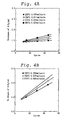
- Fig. 4 is a graph showing the relationship between the number of cycles and the thickness of the silicon oxide film when the silicon oxide film is formed using tris(dimethylamino)silane [SiH(N(CH 3 ) 2 ) 3 ] as an Si material.
- Fig. 4A shows the results when the pressure in the film-forming chamber is 0.5 Torr; and
- Fig. 4B shows the results when the pressure in the film-forming chamber is 5.0 Torr.
- Fig. 4B shows, when the film was formed under a low pressure of 0.5 Torr, the speed of forming the SiO 2 film per cycle at each substrate temperature was 0.058 nm/cycle at 225°C, 0.070 nm/cycle at 250°C, and 0.080 nm/cycle at 275°C.
- Fig. 5 is a graph showing the relationship between the number of cycles and the thickness of the Hf silicate film when a hafnium oxide (HfO 2 ) film is formed using hafnium tetramethylethylamide [Hf(N(CH 3 )(C 2 H 5 ) 2 ) 4 ] as a Hf material, and a silicon oxide (SiO 2 ) film is formed using tris(dimethylamino)silane [SiH(N(CH 3 ) 2 ) 3 ] as a Si material.
- the formation of the hafnium oxide film and the silicon oxide film is as described above.
- the pressure in the film-forming chamber in HfO 2 film formation was 0.5 Torr, and the pressure in the film-forming chamber in SiO 2 film formation was 5.0 Torr.
- the substrate temperature was 275°C.
- Hf materials and Si materials can be duly changed to the above-described other materials.
- Fig. 6 is a graph showing the relationship between the Hf/Si ratio and the Hf content in the Hf silicate film [Hf/ (Hf + Si)] in the case wherein a hafnium oxide film is formed using hafnium tetramethylethylamide [Hf(N(CH 3 )(C 2 H 5 ) 2 ) 4 ) as a Hf material and a silicon oxide film is formed using tris (dimethylamino) silane [SiH(N(CH 3 ) 2 ) 3 ] as a Si material.
- the HfO 2 film and the SiO 2 film were formed under different pressures in the film-forming chamber, and the pressure in HfO 2 film formation was 0.5 Torr and that in SiO 2 film formation was 5.0 Torr.
- the substrate temperature was 275°C.
- Fig. 6 shows, by controlling the Hf/Si ratio, that is the ratio of the number of steps for forming the HfO 2 film to the number of steps for forming the SiO 2 film in a cycle of the formation of the Hf silicate film, the Hf concentration in the Hf silicate film can be accurately controlled within a wide range of 1/30 to about 1. Therefore, byusing the above -described method, the peak concentration of the metal in the metal silicate film can be accurately controlled.
- Fig. 7 is a flow diagram for illustrating the method for manufacturing a semiconductor device according to the first embodiment.
- Figs. 8A to 10C are sectional views for illustrating the process for manufacturing a semiconductor device according to the first embodiment.
- Figs. 8A to 10C are sectional views for illustrating the process for manufacturing a PMOS transistor. Since an NMOS transistor has the similar cross-sectional structure to a PMOS transistor, the drawings illustrating the method for manufacturing an NMOS transistor will be omitted, and the process will be described when required.
- Fig. 8A shows, in the PMOS transistor-forming region, an n-type impurity is introduced into a P-type silicon substrate 1, and heat treatment is carried out to form an n-type well 2.
- a p-type impurity is introduced into the silicon substrate 1, and heat treatment is carried out to form a p-type well (Step S202).
- the PMOS and NMOS transistor-forming regions are partitioned (Step S204).
- the element-isolating region 3 is formed by forming a shallow trench in the element-isolating region of the silicon substrate 1, and burying a silicon oxide film in the trench.
- the silicon oxide film formed out of the trench can be removed using the CMP method or the etch-back method.
- a silicon oxide film 4 of a thickness of, for example, about 0.5 nm is formed on the surface of the silicon substrate 1 by a rapid heat treatment using a halogen lamp or a flash lamp (Step S208).
- an Hf silicate film 5 of a thickness of, for example, about 3 nm is formed using the above-described method (Step S210).
- a treatment for the densification of the Hf silicate film 5 may be carried out (Step S212).
- the densification treatment can be carried out, for example, by performing rapid heat treatment using a halogen lamp in a nitrogen-gas atmosphere wherein a trace of oxygen gas is added, or in a nitrogen-gas atmosphere for 1 to 600 sec.
- the densification treatment can be carried out by performing rapid heat treatment using a flash lamp in the same atmosphere for 0.8 to 20 msec.
- a nitrogen-containing Hf silicate film 6 containing Hf of a peak concentration of 1 atomic % or more and 30 atomic % or less, and nitrogen of a peak concentration of 10 atomic % or more and 30 atomic % or less is formed on the upper layer of the Hf silicate film 5 (Step S214).
- the nitrogen-containing Hf silicate film 6 can be formed by the plasma treatment using a nitrogen-based gas.
- the nitrogen-containing Hf silicate film 6 may be formed on the Hf silicate film 5 using a material that contains hafnium, oxygen, silicon and nitrogen.
- densification treatment is carried out (Step S216).
- the densification treatment can be carried out, for example, by rapid heat treatment using a lamp in a nitrogen-gas atmosphere wherein a trace of oxygen gas is added, or in a nitrogen-gas atmosphere.
- a polysilicon film 7 that will finally become a gate electrode is formed on the nitrogen-containing Hf silicate film 6 (Step S218).
- an impurity 8 such as boron is ion-implanted into the polysilicon film 7 (Step S220). Thereby, a doped polysilicon film 7a is formed on the nitrogen-containing Hf silicate film 6.
- an impurity such as phosphorus is ion-implanted into a polysilicon film formed on the NMOS transistor-forming region.
- a resist pattern (not shown) is formed on the doped polysilicon film 7a (Step S222), and using the resist pattern as a mask, the doped polysilicon film 7a, the nitrogen-containing Hf silicate film 6, the Hf silicate film 5, and the silicon oxide film 4 are sequentially etched (Step S224).
- a polysilicon gate electrode 7b is formed on the n-type well 2 of the silicon substrate 1, through the gate insulating film formed by laminating the silicon oxide film 4a, the Hf silicate film 5a, and the nitrogen-containing Hf silicate film 6a.
- a low concentration of boron difluoride (BF 2 ) is ion-implanted into the n-type well 2 using the gate electrode 7b as a mask.
- boron difluoride boron difluoride
- a p-type low-concentration ion-implanted layer 10 that will finally become an extension region is formed on the upper layer of the silicon substrate 1 on the both sides of the gate electrode 7b.
- arsenic is ion-implanted into the p-type well to form an n-type low-concentration ion-implanted layer (Step S226).
- a silicon nitride film having a thickness of, for example, about 100 nm is formed on the entire surface of the silicon substrate 1 so as to coat the gate electrode 7b, and the silicon nitride film is subjected to anisotropic etching.
- Fig. 9C shows, a sidewall 11 consisting of the silicon nitride film is formed in a self-aligning manner (Step S228).
- boron 12 is ion-implanted into the n-type well 2 as a high-concentration P-type impurity 12 using the gate electrode 7b and the sidewall 11 as masks.
- a p-type high-concentration ion-implanted layer 13 that will finally become the source/drain region is formed in the n-type well 2.
- phosphorus is ion-implanted into the p-type well to form an n-type high-concentration ion-implanted layer (Step S230).
- Step S232 rapid heat treatment using a lamp is performed (Step S232).
- Fig. 10B shows, the p-type low-concentration ion-implanted layer 10 and the p-type high-concentration ion-implanted layer 13 in the n-type well 2 are activated, and the p-type extension region 14 wherein an impurity is introduced in a low concentration, and the p-type source/drain region 15 wherein an impurity is introduced in a high concentration are formed.
- the n-type low-concentration ion-implanted layer and the n-type high-concentration ion-implanted layer in the p-type well are activated, and the n-type extension region wherein an impurity is introduced in a low concentration, and the n-type source/drain region wherein an impurity is introduced in a high concentration are formed.
- the temperature of heat treatment for activation is preferably at least 10 degrees lower than the temperature of heat treatment for densification.
- heat treatment for activation can be performed at 980°C, and heat treatment for densification can be performed at 1000°C.
- an interlayer insulating film 16 is formed on the entire surface of the substrate using the CVD method. Thereafter, a resist pattern (not shown) is formed on the insulating film 16 using a lithography techniques, contact holes connected to the source/drain region 15 are formed in the interlayer insulating film 16 by dry etching using the resist pattern as masks, and then a barrier metal film and a tungsten film are buried in the contact holes to form contacts 17. The unnecessary barrier metal film and tungsten film are removed using the CMP method. Thereafter, metal wirings 18 are formed on the contacts 17 to manufacture the semiconductor device shown in Fig. 1.
- C-V characteristics gate capacity-gate voltage characteristics
- Fig. 11 is a graph showing the C-V characteristics of a semiconductor device according to the first embodiment. Specifically, Fig. 11A is a graph showing the C-V characteristics of an NMOS transistor; and Fig. 11B is a graph showing the C-V characteristics of a PMOS transistor.
- Figs. 11A and 11B show, it is known that the C/Cmax value varies depending on the Hf /Si ratio in the reverse side, and with increase in the concentration of silicon, the C/Cmax value increases. This is considered because as the concentration of silicon in the Hf silicate film increases, the diffusion of impurities from the upper electrode polysilicon decreases, and depletion is minimized.
- the peak concentration of the metal in the nitrogen-containing Hf silicate film 6a positioned on the uppermost layer of the gate insulating film was controlled to 1 atomic % or more and 30 atomic % or less.
- the peak concentration of nitrogen in the nitrogen-containing Hf silicate film 6a was controlled to 10 atomic % or more and 30 atomic % or less. Thereby, the diffusion of impurities introduced into the gate electrode in the activating heat treatment could be inhibited, and the Vfb shift due to the diffusion of impurities could be inhibited.
- the present invention can be applied to the case of using a metal aluminate film as the high-dielectric-constant film, and using a nitrogen-containing metal aluminate film as the upper layer insulating film, and the similar results can also be obtained from this case.
- the peak concentration of the metal was equivalent in the metal silicate film 5a and in the nitrogen-containing metal silicate film 6a.
- the peak concentration of the metal in the metal silicate film 5a was higher than that in the nitrogen-containing metal silicate film 6a.
- the metal silicate film 5a was made to be a metal-rich film; and the nitrogen-containing metal silicate film 6a was made to be a silicon-rich film. Since other constitution is the same as in the above-described embodiment, the description thereof will be omitted.
- a metal silicate film e.g., Hf silicate film or Zr silicate film
- a metal silicate film as the high-dielectric-constant film 5a was made to be a metal-rich film that contains a metal in the peak concentration of 5 atomic % or more and 40 atomic % or less.
- the silicon-rich Hf silicate film is nitrided to form a silicon-rich nitrogen-containing Hf silicate film as the upper layer insulating film.
- a polysilicon film 7 is formed on the nitrogen-containing Hf silicate film.
- this modification by making the film on the uppermost layer of the gate insulating film a nitrogen-containing metal silicate film that contains the metal in the peak concentration of 1 atomic % or more and 30 atomic % or less, the similar effect as in the above-described embodiment can also be obtained. Furthermore, this modification can improve the total effective specific dielectric constant of the gate insulating film by the use of a metal-rich metal silicate film as the high-dielectric-constant film 5a.
- the semiconductor device and the method for the manufacture thereof according to the second embodiment is the same as those described in the first embodiment. In the second embodiment, however, a different method is used to form a metal silicate such as an Hf silicate.
- Fig. 12 is a schematic diagram for illustrating a thin film forming apparatus in the second embodiment of the present invention.
- the thin film forming apparatus 100 is equipped with a vacuum chamber 20.
- a table 21 is disposed on the central portion in the chamber 20, a table 21 is disposed.
- a heater 22 is installed to heat the table from the bottom thereof to a predetermined temperature.
- a gas supply pipe 23 is installed so as to pass through a portion of the outer wall of the chamber 20.
- the gas supply pipe 23 passes from the outside of the chamber 20 to the inside of the chamber 20, and thereby supplies the gas into the chamber 20.
- the gas supply pipe 23 is also disposed so as to surround upside of the table 21.
- the gas supply pipe 23 has a plurality of ejection nozzles 24. The gas supplied from the gas supply pipe 23 is ejected through these ejection nozzles 24 into the chamber 20.
- a total of two gas discharge ports 25 are installed so as to pass through the underside of the outer wall of the chamber 20.
- the gas discharge ports 25 run from the inside to the outside of the chamber 20, and are connected to a vacuum pump through a valve 26. Thereby the gas in the chamber 20 can be discharged to the exterior.
- the ceiling portion of the chamber 20, facing the table 21, is formed of a quartz window 27.
- a total of 50 flash lamps 28 are disposed, and the flash lamps 28 are covered with a reflective plate 29.
- the flash lamps 28 are connected to a capacitor 30, and the capacitor 30 is connected to a power source 31.
- the ceiling portion of the chamber 20 is formed of a quartz window 27 that permeates light so as to introduce light emitted from the flash lamps 28.
- the reflective plate 29 is installed so as to reflect the light emitted from the flash lamps 28 toward the opposite side to the chamber 20 (upward in Fig 12) to the chamber 20, and to introduce the light into the chamber 20.
- the current from the power source 31 is charged into the capacitor 30, and instant discharge of the electric charge makes the flash lamp 28 emit light.
- a metal silicate is formed using the thin film forming apparatus 100 constituted as described above, in place of the steps S102 to S110 (S210) in the manufacturing process of the semiconductor device described in the first embodiment.
- a substrate 32 is placed on the table 21.
- Fig. 13 is a flow diagram for illustrating the method for forming a metal silicate film in the second embodiment of the present invention
- Fig. 14 is a graph for illustrating the sequence in the method for forming a metal silicate film in the second embodiment.
- the metal silicate film is also formed by individually forming a hafnium oxide film and a silicon oxide film. This will be specifically described referring to Figs 12 to 14.
- a hafnium oxide film is formed.
- the table 21 is heated in the state where a substrate 32 is placed on the table 21 (Step S302).
- the table 21 is heated using the heater 22 to a temperature of 300°C.
- the temperature of the substrate 32 is maintained at 300°C.
- the gas in the chamber 20 is discharged (Step S304). Gas discharge is performed by opening the valve 26 and sucking the gas through the gas discharge ports 25 using the vacuum pump until the pressure in the chamber 20 becomes 10 -7 Torr.
- argon gas is supplied into the chamber 20 (Step S306).
- the argon gas is supplied through the gas supply pipe 23, and is ejected through the ejection nozzles 24 into the chamber 20.
- the pressure in the chamber 20 is fixed to 0.5 Torr.
- the supply of hafnium tetramethylethylamide is started at the point A 1 (Step S310).
- Hafnium tetramethylethylamide is supplied through the gas supply pipe 23, and is ejected through the ejection nozzles 24 into the chamber 20.
- the supply of hafnium tetramethylethylamide is performed at 2 sccm for 1.5 seconds, and the supply is stopped at the point B 1 1.5 seconds later (Step S312).
- Step S314) the purge of the gas in the chamber 20 is started.
- argon gas is supplied through the gas supply pipe 23 for about 5 seconds.
- the valve 26 is opened and the gas in the chamber 20 is discharged through the gas discharge ports 25 with the vacuum pump.
- the supply of argon gas and gas discharge are stopped at the point C 1 5 seconds later (Step S316). At this time, the valve 26 is closed.
- Step S3128 the supply of ozone gas is started.
- ozone gas is also supplied through the gas supply pipe 23, and is ejected through the ejection nozzles 24 into the chamber 20.
- the supply of ozone gas is performed at 5 sccm for 2 seconds, and the supply is stopped at the point D 1 2 seconds later (Step S320).
- Step S322 the discharge of the gas from the chamber 20 is started.
- the gas is purged by supplying argon gas through the gas supply pipe 23, and simultaneously the valve 26 is opened to discharge the gas through the gas discharge ports 25 using the vacuum pump.
- the light emitting of the flash lamps 28 is performed (Step S324).
- the energy of the light-emitting flash lamps 28 is 15 J/cm 2 .
- the light-emitting time of the flash lamps 28 is as an extremely short time such as about 5.0 to 20 msec, and thereby only the surface of the substrate 32 is heated instantly.
- Step S326 the supply of argon gas and the discharge of the gas from the chamber 20 are stopped. Thereafter, the introduction of hafnium tetramethylethylamide is started again (Step S310), and steps S310 to S326 are repeated.
- Step S310 and S312 the introduction of hafnium tetramethylethylamide (Steps S310 and S312), the purge of the gas (Steps S314 and S316) , the introduction of ozone gas (Steps S318 and S320), the purge of the (Steps S322 and S326) , and the light emitting of the flash lamps during the purge of the gas (Step S324) are repeated for 20 times, and the formation of the thin film is completed. Thereby, a hafnium oxide film of a thickness of about 2.5 nm can be formed on the substrate 32.
- the table 21 is maintained at about 300°C in the same manner as in the formation of the hafnium oxide film.
- the chamber 20 is purged with argon gas, and the pressure in the chamber 20 is fixed to 5.0 Torr.
- Step S330 the supply of trisdimethylaminosilane as the Si material is started at the point A 1 (Step S330).
- Trisdimethylaminosilane is supplied through the gas supply pipe 23, and is ejected through the ejection nozzles 24 into the chamber 20.
- the supply of trisdimethylaminosilane is performed at 2 sccm for 1.5 seconds, and the supply is stopped at the point B 1 1.5 seconds later (Step S332).
- Step S334 the purge of the gas in the chamber 20 is started.
- argon gas is supplied through the gas supply pipe 23 for about 5 seconds, and on the other hand, the valve 26 is opened.
- the gas in the chamber 20 is discharged through the gas discharge ports 25 with the vacuum pump, and the purge of the gas is stopped at the point C 1 5 seconds later (Step S336).
- Step S328 the supply of ozone gas is started.
- ozone gas is also supplied through the gas supply pipe 23, and is ejected through the ejection nozzles 24 into the chamber 20.
- the supply of ozone gas is performed at 5 sccm for 2 seconds, and the supply is stopped at the point D 1 2 seconds later (Step S340).
- Step S342 the discharge of the gas from the chamber 20 is started.
- the gas is purged by supplying argon gas through the gas supply pipe 23, and simultaneously the valve 26 is opened to discharge the gas through the gas discharge ports 25 using the vacuum pump.
- the light emitting of the flash lamps 28 is performed (Step S344).
- the energy of the light-emitting flash lamps 28 is 15 J/cm 2 .
- the light-emitting time of the flash lamps 28 is as an extremely short time such as about 5.0 to 20 msec, and thereby only the surface of the substrate 32 is heated instantly.
- Step S346 the purge of the gas in the chamber 20 is stopped. Thereafter, the introduction of trisdimethylaminosilane is started again (Step S330), and steps S330 to S346 are repeated.
- Step S330 and S332 the introduction of trisdimethylaminosilane (Steps S330 and S332), the purge of the gas (Steps S334 and S336), the introduction of ozone gas (Steps S338 and S340), the purge of the gas (Steps S342 and S346), and the light emitting of the flash lamps 28 during the purge of the gas (Step S344) are repeated for 5 times, and the formation of the thin film is completed. Thereby, a silicon oxide film of a thickness of about 0.4 nm can be formed on the substrate 32.
- the formed hafnium oxide film in the second embodiment was compared with an aluminum oxide film formed according to a conventional method, wherein the sequence of the supply of the material gas and the purge of the gas is performed in the same manner, but without heating with the flash lamps 28, using a secondary ion mass spectrometer, and it was found that the quantity of residual carbon in the thin film was lowered to about 1/10.
- heating of the millisecond order can be performed by heating by flash lamps, the temperature of the surface of the substrate 32 can be raised instantly to accelerate the reaction, and the temperature of the substrate 32 can be immediately lowered to the original temperature.
- an oxidizing gas such as ozone gas is supplied to start oxidation reaction.
- the temperature of the wafer is low, and the reaction time is not sufficiently long, the oxidation reaction is not completed. This is considered to be the cause of residual impurities in the film.
- the flash lamps 28 can heat the surface of a wafer for the millisecond order and can raise the surface temperature of the wafer instantly to accelerate the rate of reaction. Also since only the surface of the substrate 32 is heated for an extremely short time, the wafer temperature can be immediately returned to the original temperature. Therefore, the next cycle (Steps S310 to S324) can be performed at the original wafer temperature. Thereby, a high-dielectric-constant thin film having a low impurity concentration and good characteristics can be formed.
- the present invention is not limited thereto, but the thin film forming apparatus 100 can be applied to the formation of other thin films.
- the thin film forming apparatus of the present invention is not limited to the apparatus using 50 flash lamps.
- flash lamps 28 are used as the heating means.
- the heating means in the present invention is not limited to the flash lamps, but other means can be used as long as the surface of the substrate can be adequately heated.
- the heating time by the flash lamps is 5.0 to 20 milliseconds.
- the heating time in the present invention is not limited to this range.
- the heating time is preferably 0.8 milliseconds or longer.
- the upper portion of the chamber 20 was made to be a quartz window 27, through which light from the flash lamps 28 was transmitted to irradiate the substrate in the chamber 20. Furthermore, the case wherein a reflective plate 29 is installed above the flash lamps 28 so as to reflect light emitted upward and irradiate the chamber 20 was described.
- the constitution of the thin film forming apparatus according to the present invention is not limited thereto, but other constitution, for example, the constitution wherein the flash lamps 28 are directly installed in the chamber 20, can be used.
- the thin film forming apparatus of the present invention is not limited to the apparatus having such a constitution, but other constitutions can be used as long as the gas can be supplied into the chamber 20, and the gas can be adequately discharged from the chamber 20.
- the other constitutions of the thin film forming apparatus of the present invention are not limited to the constitution described in this embodiment, but other constitutions can be used as long as the surface of the substrate can be adequately heated, and the reaction can be accelerated.
- the metal content in the metal silicate film formed on the uppermost layer of a high-dielectric-constant film is controlled. Accordingly, the semiconductor device having C-V characteristics equivalent to ideal C-V characteristics can be realized.
Landscapes
- Insulated Gate Type Field-Effect Transistor (AREA)
- Metal-Oxide And Bipolar Metal-Oxide Semiconductor Integrated Circuits (AREA)
- Formation Of Insulating Films (AREA)
Applications Claiming Priority (2)
| Application Number | Priority Date | Filing Date | Title |
|---|---|---|---|
| JP2003434367 | 2003-12-26 | ||
| JP2003434367A JP2005191482A (ja) | 2003-12-26 | 2003-12-26 | 半導体装置及びその製造方法 |
Publications (1)
| Publication Number | Publication Date |
|---|---|
| EP1548839A1 true EP1548839A1 (de) | 2005-06-29 |
Family
ID=34545101
Family Applications (1)
| Application Number | Title | Priority Date | Filing Date |
|---|---|---|---|
| EP04006409A Withdrawn EP1548839A1 (de) | 2003-12-26 | 2004-03-17 | Halbleiterbauelement und Verfahren zu deren Herstellung, Vorrichtung und Verfahren zur Herstellung eines Films mit hoher Dielektrizitätskonstante |
Country Status (4)
| Country | Link |
|---|---|
| US (2) | US7101753B2 (de) |
| EP (1) | EP1548839A1 (de) |
| JP (1) | JP2005191482A (de) |
| KR (1) | KR20050066936A (de) |
Cited By (9)
| Publication number | Priority date | Publication date | Assignee | Title |
|---|---|---|---|---|
| EP1862566A1 (de) * | 2006-05-30 | 2007-12-05 | Air Products and Chemicals, Inc. | Diethylsilan als Siliciumquelle bei der Abscheidung von Metallsilikatschichten |
| EP1939323A1 (de) * | 2006-12-13 | 2008-07-02 | Air Products and Chemicals, Inc. | Zyklische chemische Dampfphasenabscheidung von Metall-Silizium-haltigen Schichten |
| WO2008042695A3 (en) * | 2006-09-29 | 2008-10-16 | Tokyo Electron Ltd | Semiconductor devices containing nitrided high dielectric constant films and method of forming |
| US7759746B2 (en) | 2006-03-31 | 2010-07-20 | Tokyo Electron Limited | Semiconductor device with gate dielectric containing aluminum and mixed rare earth elements |
| US7767262B2 (en) | 2006-09-29 | 2010-08-03 | Tokyo Electron Limited | Nitrogen profile engineering in nitrided high dielectric constant films |
| US7816737B2 (en) | 2006-03-31 | 2010-10-19 | Tokyo Electron Limited | Semiconductor device with gate dielectric containing mixed rare earth elements |
| US8012442B2 (en) | 2006-03-31 | 2011-09-06 | Tokyo Electron Limited | Method of forming mixed rare earth nitride and aluminum nitride films by atomic layer deposition |
| US8076241B2 (en) | 2009-09-30 | 2011-12-13 | Tokyo Electron Limited | Methods for multi-step copper plating on a continuous ruthenium film in recessed features |
| US8097300B2 (en) | 2006-03-31 | 2012-01-17 | Tokyo Electron Limited | Method of forming mixed rare earth oxynitride and aluminum oxynitride films by atomic layer deposition |
Families Citing this family (26)
| Publication number | Priority date | Publication date | Assignee | Title |
|---|---|---|---|---|
| KR100876927B1 (ko) * | 2001-06-01 | 2009-01-07 | 가부시키가이샤 한도오따이 에네루기 켄큐쇼 | 열처리장치 및 열처리방법 |
| KR100689824B1 (ko) * | 2004-05-14 | 2007-03-08 | 삼성전자주식회사 | 원자층 증착 기술을 이용한 금속 실리케이트막 형성 방법 |
| US8323754B2 (en) * | 2004-05-21 | 2012-12-04 | Applied Materials, Inc. | Stabilization of high-k dielectric materials |
| US7564108B2 (en) * | 2004-12-20 | 2009-07-21 | Taiwan Semiconductor Manufacturing Company, Ltd. | Nitrogen treatment to improve high-k gate dielectrics |
| KR100688521B1 (ko) * | 2005-01-18 | 2007-03-02 | 삼성전자주식회사 | 고유전율 절연막을 포함하는 반도체 소자 및 그 제조 방법 |
| JP2006261434A (ja) | 2005-03-17 | 2006-09-28 | L'air Liquide Sa Pour L'etude & L'exploitation Des Procede S Georges Claude | シリコン酸化膜の形成方法 |
| JP4671729B2 (ja) * | 2005-03-28 | 2011-04-20 | 富士通セミコンダクター株式会社 | 半導体装置及びその製造方法 |
| JP4554446B2 (ja) * | 2005-06-21 | 2010-09-29 | ルネサスエレクトロニクス株式会社 | 半導体装置の製造方法 |
| US7655994B2 (en) * | 2005-10-26 | 2010-02-02 | International Business Machines Corporation | Low threshold voltage semiconductor device with dual threshold voltage control means |
| JP2007235093A (ja) * | 2006-01-31 | 2007-09-13 | Toshiba Corp | 半導体装置の製造方法 |
| US7601651B2 (en) * | 2006-03-31 | 2009-10-13 | Applied Materials, Inc. | Method to improve the step coverage and pattern loading for dielectric films |
| US20080001237A1 (en) * | 2006-06-29 | 2008-01-03 | Taiwan Semiconductor Manufacturing Company, Ltd. | Semiconductor device having nitrided high-k gate dielectric and metal gate electrode and methods of forming same |
| KR100744423B1 (ko) | 2006-08-28 | 2007-07-30 | 동부일렉트로닉스 주식회사 | 하프늄 실리케이트 산화막 형성 방법 및 이를 이용한반도체 소자의 제조 방법 |
| JP2008135726A (ja) * | 2006-10-23 | 2008-06-12 | Interuniv Micro Electronica Centrum Vzw | 主電極を含むドープされた金属を含む半導体装置 |
| KR100864871B1 (ko) * | 2007-05-29 | 2008-10-22 | 한국전자통신연구원 | 반도체 소자 제조방법 |
| US8159035B2 (en) * | 2007-07-09 | 2012-04-17 | Taiwan Semiconductor Manufacturing Co., Ltd. | Metal gates of PMOS devices having high work functions |
| US7998820B2 (en) * | 2007-08-07 | 2011-08-16 | Taiwan Semiconductor Manufacturing Company, Ltd. | High-k gate dielectric and method of manufacture |
| US7858535B2 (en) * | 2008-05-02 | 2010-12-28 | Micron Technology, Inc. | Methods of reducing defect formation on silicon dioxide formed by atomic layer deposition (ALD) processes and methods of fabricating semiconductor structures |
| KR101451716B1 (ko) * | 2008-08-11 | 2014-10-16 | 도쿄엘렉트론가부시키가이샤 | 성막 방법 및 성막 장치 |
| US8129284B2 (en) * | 2009-04-28 | 2012-03-06 | Dainippon Screen Mfg. Co., Ltd. | Heat treatment method and heat treatment apparatus for heating substrate by light irradiation |
| JP5247619B2 (ja) * | 2009-07-28 | 2013-07-24 | キヤノンアネルバ株式会社 | 誘電体膜、誘電体膜を用いた半導体装置の製造方法及び半導体製造装置 |
| EP2823083B1 (de) * | 2012-03-09 | 2023-10-04 | Versum Materials US, LLC | Verfahren zur herstellung von silikonhaltigen filmen auf dünnfilmtransistorvorrichtungen |
| JP5955658B2 (ja) * | 2012-06-15 | 2016-07-20 | 株式会社Screenホールディングス | 熱処理方法および熱処理装置 |
| WO2016109667A1 (en) | 2014-12-31 | 2016-07-07 | Servicenow, Inc. | Permitted assignment user interface |
| US10769826B2 (en) | 2014-12-31 | 2020-09-08 | Servicenow, Inc. | Visual task board visualization |
| TWI797640B (zh) | 2020-06-18 | 2023-04-01 | 法商液態空氣喬治斯克勞帝方法研究開發股份有限公司 | 基於矽之自組裝單層組成物及使用該組成物之表面製備 |
Citations (2)
| Publication number | Priority date | Publication date | Assignee | Title |
|---|---|---|---|---|
| EP1363333A1 (de) * | 2001-06-21 | 2003-11-19 | Matsushita Electric Industrial Co., Ltd. | Halbleiterbauelement und verfahren zu seiner herstellung |
| US20030218223A1 (en) * | 2002-02-26 | 2003-11-27 | Kabushiki Kaisha Toshiba | Semiconductor device and its manufacturing method |
Family Cites Families (16)
| Publication number | Priority date | Publication date | Assignee | Title |
|---|---|---|---|---|
| US5705224A (en) | 1991-03-20 | 1998-01-06 | Kokusai Electric Co., Ltd. | Vapor depositing method |
| CN100465742C (zh) * | 1992-08-27 | 2009-03-04 | 株式会社半导体能源研究所 | 有源矩阵显示器 |
| US6020243A (en) | 1997-07-24 | 2000-02-01 | Texas Instruments Incorporated | Zirconium and/or hafnium silicon-oxynitride gate dielectric |
| FI117979B (fi) | 2000-04-14 | 2007-05-15 | Asm Int | Menetelmä oksidiohutkalvojen valmistamiseksi |
| US6544906B2 (en) | 2000-12-21 | 2003-04-08 | Texas Instruments Incorporated | Annealing of high-k dielectric materials |
| JP2002299607A (ja) * | 2001-03-28 | 2002-10-11 | Toshiba Corp | Mis型電界効果トランジスタ及びこれの製造方法 |
| JP2002343790A (ja) | 2001-05-21 | 2002-11-29 | Nec Corp | 金属化合物薄膜の気相堆積方法及び半導体装置の製造方法 |
| US6642131B2 (en) | 2001-06-21 | 2003-11-04 | Matsushita Electric Industrial Co., Ltd. | Method of forming a silicon-containing metal-oxide gate dielectric by depositing a high dielectric constant film on a silicon substrate and diffusing silicon from the substrate into the high dielectric constant film |
| JP3773448B2 (ja) * | 2001-06-21 | 2006-05-10 | 松下電器産業株式会社 | 半導体装置 |
| WO2003019643A1 (fr) * | 2001-08-23 | 2003-03-06 | Nec Corporation | Dispositif semi-conducteur comportant un film isolant presentant une permittivite elevee et son procede de production |
| JP4102072B2 (ja) * | 2002-01-08 | 2008-06-18 | 株式会社東芝 | 半導体装置 |
| JP4095326B2 (ja) * | 2002-03-29 | 2008-06-04 | 株式会社東芝 | 半導体装置の製造方法及び半導体装置 |
| JP3627106B2 (ja) * | 2002-05-27 | 2005-03-09 | 株式会社高純度化学研究所 | 原子層吸着堆積法によるハフニウムシリケート薄膜の製造方法 |
| JP2004186567A (ja) * | 2002-12-05 | 2004-07-02 | Toshiba Corp | 半導体装置および半導体装置の製造方法 |
| AU2003213420A1 (en) * | 2003-03-17 | 2004-10-11 | Fujitsu Limited | Semiconductor device and method for manufacturing semiconductor device |
| JP4059183B2 (ja) * | 2003-10-07 | 2008-03-12 | ソニー株式会社 | 絶縁体薄膜の製造方法 |
-
2003
- 2003-12-26 JP JP2003434367A patent/JP2005191482A/ja active Pending
-
2004
- 2004-03-17 EP EP04006409A patent/EP1548839A1/de not_active Withdrawn
- 2004-03-30 US US10/811,979 patent/US7101753B2/en not_active Expired - Fee Related
- 2004-03-30 KR KR1020040021385A patent/KR20050066936A/ko not_active Withdrawn
-
2006
- 2006-06-29 US US11/476,867 patent/US20060273408A1/en not_active Abandoned
Patent Citations (2)
| Publication number | Priority date | Publication date | Assignee | Title |
|---|---|---|---|---|
| EP1363333A1 (de) * | 2001-06-21 | 2003-11-19 | Matsushita Electric Industrial Co., Ltd. | Halbleiterbauelement und verfahren zu seiner herstellung |
| US20030218223A1 (en) * | 2002-02-26 | 2003-11-27 | Kabushiki Kaisha Toshiba | Semiconductor device and its manufacturing method |
Non-Patent Citations (2)
| Title |
|---|
| HU H ET AL: "MIM CAPACITORS USING ATOMIC-LAYER-DEPOSITED HIGH-K (HFO2)1-X(ALO3)X DIELECTRICS", IEEE ELECTRON DEVICE LETTERS, IEEE INC. NEW YORK, US, vol. 24, no. 2, February 2003 (2003-02-01), pages 60 - 62, XP001157957, ISSN: 0741-3106 * |
| VAINONEN-AHLGREN E ET AL: "Atomic layer deposition of hafnium and zirconium silicate thin films", COMPUT MATER SCI; COMPUTATIONAL MATERIALS SCIENCE MARCH 2003, vol. 27, no. 1-2, 18 June 2002 (2002-06-18), pages 65 - 69, XP002295371 * |
Cited By (11)
| Publication number | Priority date | Publication date | Assignee | Title |
|---|---|---|---|---|
| US7759746B2 (en) | 2006-03-31 | 2010-07-20 | Tokyo Electron Limited | Semiconductor device with gate dielectric containing aluminum and mixed rare earth elements |
| US7816737B2 (en) | 2006-03-31 | 2010-10-19 | Tokyo Electron Limited | Semiconductor device with gate dielectric containing mixed rare earth elements |
| US8012442B2 (en) | 2006-03-31 | 2011-09-06 | Tokyo Electron Limited | Method of forming mixed rare earth nitride and aluminum nitride films by atomic layer deposition |
| US8097300B2 (en) | 2006-03-31 | 2012-01-17 | Tokyo Electron Limited | Method of forming mixed rare earth oxynitride and aluminum oxynitride films by atomic layer deposition |
| EP1862566A1 (de) * | 2006-05-30 | 2007-12-05 | Air Products and Chemicals, Inc. | Diethylsilan als Siliciumquelle bei der Abscheidung von Metallsilikatschichten |
| US7582574B2 (en) | 2006-05-30 | 2009-09-01 | Air Products And Chemicals, Inc. | Diethylsilane as a silicon source in the deposition of metal silicate films |
| WO2008042695A3 (en) * | 2006-09-29 | 2008-10-16 | Tokyo Electron Ltd | Semiconductor devices containing nitrided high dielectric constant films and method of forming |
| US7767262B2 (en) | 2006-09-29 | 2010-08-03 | Tokyo Electron Limited | Nitrogen profile engineering in nitrided high dielectric constant films |
| EP1939323A1 (de) * | 2006-12-13 | 2008-07-02 | Air Products and Chemicals, Inc. | Zyklische chemische Dampfphasenabscheidung von Metall-Silizium-haltigen Schichten |
| US7678422B2 (en) | 2006-12-13 | 2010-03-16 | Air Products And Chemicals, Inc. | Cyclic chemical vapor deposition of metal-silicon containing films |
| US8076241B2 (en) | 2009-09-30 | 2011-12-13 | Tokyo Electron Limited | Methods for multi-step copper plating on a continuous ruthenium film in recessed features |
Also Published As
| Publication number | Publication date |
|---|---|
| US20050139937A1 (en) | 2005-06-30 |
| KR20050066936A (ko) | 2005-06-30 |
| US7101753B2 (en) | 2006-09-05 |
| US20060273408A1 (en) | 2006-12-07 |
| JP2005191482A (ja) | 2005-07-14 |
Similar Documents
| Publication | Publication Date | Title |
|---|---|---|
| US7101753B2 (en) | Method for manufacturing a semiconductor device and method for forming high-dielectric-constant film | |
| US8334198B2 (en) | Method of fabricating a plurality of gate structures | |
| US7622401B2 (en) | Method of producing insulator thin film, insulator thin film, method of manufacturing semiconductor device, and semiconductor device | |
| US7153786B2 (en) | Method of fabricating lanthanum oxide layer and method of fabricating MOSFET and capacitor using the same | |
| JP4863296B2 (ja) | 半導体装置の製造方法 | |
| US8350335B2 (en) | Semiconductor device including off-set spacers formed as a portion of the sidewall | |
| JP4554446B2 (ja) | 半導体装置の製造方法 | |
| KR20110008209A (ko) | 붕소 질화물 및 붕소-질화물 유도 물질들 증착 방법 | |
| US9385208B2 (en) | Semiconductor device having high-K gate dielectric layer | |
| US20050051857A1 (en) | Semiconductor device | |
| US8163626B2 (en) | Enhancing NAND flash floating gate performance | |
| JP2005032908A (ja) | 薄膜の形成方法 | |
| KR20120089147A (ko) | 반도체 소자의 제조 방법 | |
| KR100647484B1 (ko) | 박막 제조 방법 및 이를 이용한 게이트 구조물,커패시터와 플래시 메모리 장치의 제조 방법 | |
| US20060273320A1 (en) | Method of manufacturing semiconductor device | |
| EP1796174A1 (de) | Stark dielektrischer film und feldeffekttransistor und integrierte halbleiter-schaltungsvorrichtung damit und prozess zur herstellung des stark dielektrischen films | |
| JP2004247474A (ja) | 半導体装置及びその製造方法並びに成膜方法 | |
| KR20050001429A (ko) | 반도체 장치 및 그 제조 방법 | |
| KR20060070010A (ko) | 박막 제조 방법 및 이를 이용한 게이트 구조물,커패시터와 플래시 메모리 장치의 제조 방법 |
Legal Events
| Date | Code | Title | Description |
|---|---|---|---|
| PUAI | Public reference made under article 153(3) epc to a published international application that has entered the european phase |
Free format text: ORIGINAL CODE: 0009012 |
|
| AK | Designated contracting states |
Kind code of ref document: A1 Designated state(s): AT BE BG CH CY CZ DE DK EE ES FI FR GB GR HU IE IT LI LU MC NL PL PT RO SE SI SK TR |
|
| AX | Request for extension of the european patent |
Extension state: AL LT LV MK |
|
| RAP1 | Party data changed (applicant data changed or rights of an application transferred) |
Owner name: NEC ELECTRONICS CORPORATION |
|
| AKX | Designation fees paid | ||
| STAA | Information on the status of an ep patent application or granted ep patent |
Free format text: STATUS: THE APPLICATION IS DEEMED TO BE WITHDRAWN |
|
| 18D | Application deemed to be withdrawn |
Effective date: 20051230 |
|
| REG | Reference to a national code |
Ref country code: DE Ref legal event code: 8566 |