BACKGROUND OF THE INVENTION
Field of the Invention
The present invention relates to a semiconductor device using
a metal silicate film as a gate insulating film, to a method for
manufacturing such a semiconductor device, to an apparatus being
available for forming film in such a semiconductor device, and
to method being available for forming high-dielectric-constant
film in such a semiconductor device.
Background Art
Accompanying the miniaturization of semiconductor devices,
the reduction of thickness of gate insulating films has been
demanded. The reduction of thickness of silicon oxide films and
silicon oxynitride films (hereafter referred to as "silicon oxide
film and the like" ) , which are used as conventional gate insulating
films, is limited due to increase in leak current, and it is
difficult to reduce the SiO2-converte film thickness to 1.5 nm
or less. Therefore, there has been proposed a method for
inhibiting leak current by using a high-dielectric-constantfilm,
such as a metal oxide film, a metal silicate film and a metal
aluminate film, which has a higher specific inductive capacity
higher than that of silicon oxide film and the like as the gate
insulating film; and by increasing the physical film thickness
of the gate insulating film.
However, when the high-dielectric-constant film is used as
the gate insulating film, and a polysilicon electrode is used
as the gate electrode, there has been a problem that impurities
doped in the polysilicon electrode diffuse into the substrate
through the gate insulating film when the impurities are activated,
and the transistor properties are deteriorated.
In order to solve this problem, a method for introducing
nitrogen into the high-dielectric-constant film has been
proposed.
Specifically, there has been proposed a method for forming
a high-dielectric-constant film composed of a zirconium
oxynitride layer or a hafnium oxynitride layer, by forming a metal
layer composed of zirconium or hafnium on a substrate, and
oxynitriding the metal layer (refer to e.g., Japanese Patent
Laid-Open No. 2000-58832).
Furthermore, there has also been proposed a method for
laminating a lower barrier film consisting of ahafnium-containing
silicon oxynitride film, a high-dielectric-constant film
consisting of a silicon-containing hafnium oxide film, and an
upper barrier film consisting of a silicon-containing hafnium
oxide film that contains nitrogen to form a gate insulating film
and for controlling the composition of a metal (M), oxygen (O),
nitrogen (N) and silicon (Si) in the high-dielectric-constant
film and the lower barrier film (refer to e.g., Japanese Patent
Laid-Open No. 2003-8011).
In a thin-film formation using a high-dielectric-constant
material, the ALD (atomic layer deposition) method is generally
used. In this method, material gasses are alternately supplied
while resetting the chamber to the original state to form each
atomic layer.
For example, the formation of a hafnium oxide (HfO2) film
as a high-dielectric-constant filmwill be specifically described.
First, the chamber is evacuated, argon gas is flowed in the chamber,
and the pressure in the chamber is maintained to 0.2 Torr. In
this state, hafnium tetramethylethylamide [Hf(N(CH3)(C2H5)2)4]
is flowed into the chamber while controlling the flow rate, and
the Hf material is vaporized and adsorbed on the surface of the
substrate. Then, the chamber is purged, and an oxidizing gas
such as ozone gas is introduced. Thereafter, the chamber is purged.
By repeating such steps for several tens of times, a hafnium oxide
(HfO2) film of a thickness of several nanometers can be formed
on the surface of the substrate.
The introduction of nitrogen into a high-dielectric-constant
film reduces flat-band-voltage shift (hereafter
referred to as "Vfb shift") due to the diffusion of impurities.
This is estimated because the high-dielectric-constant gate
insulating film is densified by nitriding treatment, and the
diffusion of impurities is restricted.
However, in the above-described conventional method,
initial Vfb shift due to the effect of fixed charge or the like
is large, and there has been a problem that satisfactory transistor
characteristics cannot obtained particularly in P-channel MIS
transistors.
In addition, a high-dielectric-constant thin film formed
using the ALD method generally contains several percent impurities.
This is considered because carbon (C), hydrogen (H) or chlorine
(C1) included in material gas using the ALD method remains and
is incorporated in the formed film. The impurities remaining
in the high-dielectric-constant film may cause fixed charge and
trap, and the characteristics of the film is damaged.
SUMMARY OF THE INVENTION
The one object of the present invention is to restrict initial
Vfb shift, to form a gate insulating film having high film quantity,
and to achieve satisfactory transistor characteristics.
Another object of the present invention is to lower the
impurity content in the high-dielectric-constant film of the gate
insulating film.
According to one aspect of the present invention, a
semiconductor device comprises a substrate, a gate insulating
film and a gate electrode. The gate insulating film is formed
on the substrate, and has a nitrogen-containing metal silicate
film or a nitrogen-containing metal aluminate film that contains
a metal in a peak concentration of 1 atomic % or more and 30 atomic %
or less on the uppermost layer. The gate electrode is formed on
the gate insulating film.
Another aspect of the present invention, a semiconductor
device comprises a substrate, a gate insulating film, and a gate
electrode. The gate insulating film is formed on the substrate
and has a base interface layer, a metal silicate film and a
nitrogen-containing metal silicate film. The base interface
layer is formed on the substrate. The metal silicate film is
formed on the base interface layer, and contains a metal, oxygen
and silicon. The nitrogen-containing metal silicate film
contains a metal in a peak concentration of 1 atomic % or more
and 30 atomic % or less, oxygen, silicon, and nitrogen. The gate
electrode formed on the gate insulating film.
Another aspect of the present invention, in method for
manufacturing a semiconductor device, a base interface layer is
formed on a substrate. A metal silicate film containing a metal
in a peak concentration of 1 atomic % or more and 30 atomic %
or less is formed on the base interface layer. A
nitrogen-containing metal silicate film containing nitrogen in
a peak concentration of 10 atomic % or more and 30 atomic % or
less is formed on the upper layer of the metal silicate film.
A gate electrode is formed on the nitrogen-containing metal
silicate film.
Another aspect of the present invention, in method for
manufacturing a semiconductor device, a base interface layer is
formed on a substrate. A metal silicate film containing a metal
in a peak concentration of 5 atomic % or more and 40 atomic %
or less is formed on the base interface layer. A
nitrogen-containing metal silicate film containing a metal in
a peak concentration of 1 atomic % or more and 30 atomic % or
less and nitrogen in a peak concentration of 10 atomic % or more
and 30 atomic % or less is formed on the metal silicate film.
A gate electrode is formed on the nitrogen-containing metal
silicate film.
Another aspect of the present invention, a apparatus for
forming a film comprises a housing, a table installed in the housing,
for placing a substrate, a gas supply port for supplying a gas
into the housing, a gas discharge port for discharging the gas
in the housing out of the housing, and a heater. The heater is
for heating the surface of the substrate by radiating light on
the surface of the substrate placed on the table for a time up
to several milliseconds.
Another aspect of the present invention, in a method for
forming a high-dielectric-constant film on a substrate, a first
material gas that contains at least one element in elements
constituting the high-dielectric-constant film is supplied into
a housing wherein the substrate is placed. A second material
gas that reacts with the first material gas and forms the
high-dielectric-constant film is supplied into the housing. The
surface of the substrate is heated by radiating light onto the
surface of the substrate for a time up to several milliseconds.
Other and further objects, features and advantages of the
invention will appear more fully from the following description.
Brief Description of the Drawings
Fig. 1 is a sectional view for illustrating a semiconductor
device in the first embodiment of the present invention;
Fig. 2 is a flow diagram for illustrating a method for forming
a metal silicate film in the first embodiment of the present
invention;
Fig. 3 is a graph showing the relationship between the number
of cycles and the thickness of the hafnium oxide film when the
hafnium oxide film is formed using tetramethylethylamide as an
Hf material;
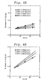
Fig. 4A and 4B are graphs showing the relationship between
the number of cycles and the thickness of the silicon oxide film
when the silicon oxide film is formed using
tris(dimethylamino)silane [SiH(N(CH3)2)3] as an Si material;
Fig. 5 is a graph showing the relationship between the number
of cycles and the thickness of the Hf silicate film when a hafnium
oxide film is formed using hafnium tetramethylethylamide
[Hf(N(CH3)(C2Hs)2)4] as a Hf material, and a silicon oxide film
is formed using tris(dimethylamino)silane [SiH(N(CH3)2)3] as a
Si material;
Fig. 6 is a graph showing the relationship between the Hf/Si
ratio and the Hf content in the Hf silicate film [Hf/(Hf + Si)]
in the case wherein a hafnium oxide film is formed using hafnium
tetramethylethylamide [Hf(N(CH3)(C2H5)2)4] as a Hf material and
a silicon oxide film is formed using tris(dimethylamino)silane
[SiH(N(CH3)2)3] as a Si material;
Fig. 7 is a flow diagram for illustrating the method for
manufacturing a semiconductor device in the first embodiment of
the present invention;
Figs. 8A to 10C are sectional views for illustrating the
process for manufacturing a semiconductor device in the first
embodiment of the present invention;
Fig. 11A and 11B are a graphs showing the C-V characteristics
of a semiconductor device in the first embodiment of the present
invention;
Fig. 12 is a schematic diagram for illustrating a thin film
forming apparatus in the second embodiment of the present
invention;
Fig. 13 is a flow diagram for illustrating the method for
forming a metal silicate film in the second embodiment of the
present invention; and
Fig. 14 is a graph for illustrating the sequence in the method
for forming a metal silicate film in the second embodiment.
Detailed Description of the Preferred Embodiments
The embodiment of the present invention will be described
referring to the drawings. In each of the drawings, the same
or like parts will be denoted with the same reference numerals,
and the description thereof will be simplified or omitted.
First Embodiment
Fig. 1 is a sectional view for illustrating a semiconductor
device according to the first embodiment of the present invention.
Specifically, Fig. 1 is a sectional view for illustrating a
P-channel MOS transistor (hereafter referred to as "PMOS
transistor").
In the PMOS, a substrate 1 is a p-type silicon substrate.
As Fig. 1 shows, an n-type well 2 to which an n-type impurity
is introduced is formed in the substrate 1. An element-isolating
structure 3 is formed on the element-isolating region of the
substrate 1. By the element-isolating structure 3, a PMOS
transistor-forming region, which is an active region, is
partitioned. The element-isolating structure 3 is an STI
(shallow trench isolation) formed by filling a shallow trench
formed from the surface side of the substrate 1 with a silicon
oxide film. On the substrate 1 of the MOS transistor-forming
region, gate insulating films 4a, 5a and 6a are laminated and
a gate electrode 7b is formed through the gate insulating films
4a, 5a and 6a.
The gate insulating film has a base interface layer 4a formed
on the substrate 1, a high-dielectric-constant film 5a formed
on the base interface layer 4a, and an upper layer insulating
film 6a formed on the high-dielectric-constant film 5a. The base
interface layer 4a is silicon oxide film for repressing the
reaction at the interface. The thickness of the base interface
layer 4a is preferably 1 nm or below, for example, about 0.5 nm.
The high-dielectric-constant film 5a is a metal silicate
film that contains a metal, oxygen and silicon, and for example,
an Hf (hafnium) silicate film or a Zr (zirconium) silicate film
can be used. The thickness of the high-dielectric-constant film
5a is, for example, about 3 nm.
The upper layer insulating film 6a is a nitrogen-containing
metal silicate film that contains a metal, oxygen, silicon and
nitrogen, and for example, a nitrogen-containing Hf silicate film
or a nitrogen-containing Zr silicate film can be used.
The upper layer insulating film 6a is a film containing a
metal such as Hf and Zr in a peak concentration of 1 atomic %
or more and 30 atomic % or less. That is, the nitrogen-containing
metal silicate film 6a is a silicon-rich film. This is because
if the peak concentration of the metal exceeds 30 atomic %,
satisfactory electrical properties cannot be obtained as
described later.
The upper layer insulating film 6a also contains nitrogen
in a peak concentration of 10 atomic % or more and 30 atomic %
or less. This is because if the peak concentration of nitrogen
is less than 10 atomic %, the densification of the upper layer
insulating film 6a becomes insufficient, and in the activating
heat treatment, the inhibition of the diffusion of impurities
such as phosphorus and boron introduced into polysilicon, which
is the gate electrode, becomes difficult to control. It is
practically impossible to make the peak concentration of nitrogen
exceed 30 atomic %, and even if it is possible, excellent electrical
properties cannot be obtained.
The thickness of the upper layer insulating film 6a is
preferably about 1/20 to 2/3 the thickness of the
high-dielectric-constant film 5a.
The gate electrode 7b is a polysilicon electrode consisting
of a doped silicon film formed by introducing an impurity into
a polysilicon film. The polysilicon electrode can be substituted
by a silicon-germanium (SixGey) can be used as the gate electrode
7b.
On the sides of the gate electrode 7b, and gate insulating
films 4a, 5a and 6a, a sidewall 11 is formed as a spacer for forming
LDD. The sidewall 11 consists of a silicon oxide film or a silicon
nitride film.
Across the channel region on the surface of the substrate
1 below the gate electrode 7b, an extension region 14 of lower
concentration is formed by introducing a p-type impurity. A
source-drain region 15 of higher concentration is formed by
introducing a p-type impurity on the n-type well 2 so as to connect
to the extension region 14.
An interlayer insulating film 16, such as BPSG, BSG and PSG,
is formed so as to coat the gate electrode 7b. In the interlayer
insulating film 16, contact hole connected to the source-drain
region 15 are formed, and in the contact holes, contacts 17, in
which conductive films such as a laminated films of barrier metal
films and tungsten films are buried, are formed. Metal wirings
18 are formed on the contacts 17.
The present invention can be applied not only to the
above-described PMOS transistor, but also to an N-type channel
MOS transistor ( hereafter referred to as "NMOS transistor" ) having
the same cross-sectional structure.
In the case of an NMOS transistor, a p-type well is formed
in a p-type substrate 1, and an NMOS transistor-forming region
is partitioned by an element isolating structure 3. Furthermore,
in the p-type well, an extension region of a lower concentration
formed by introducing an n-type impurity, and a source-drain
region of a higher concentration formed by introducing an n-type
impurity and connected to the extension are formed.
Fig. 2 is a flow diagram for illustrating a method for forming
a metal silicate film in the second embodiment of the present
invention.
The method for forming a metal silicate film as the
above-described high-dielectric-constant film 5 will be
described below referring to Fig. 2. Specifically, a method for
forming an Hf silicate film will be described.
The Hf silicate film is formed by the combination of a step
for forming a hafnium oxide film (HfO2 film) using the ALD (atomic
layer deposition) method, and a step for forming a silicon oxide
film (SiO2 film) using the ALD method, and by controlling the
number of each step.
The details of each step will be described below.
First, the step for forming a hafnium oxide film will be
described.
The hafnium oxide film is formed by controlling the flow
rate of hafnium tetramethylethylamide [Hf(N(CH3)(C2H5)2)4] as an
Hf material using a mass flow controller, gasifying the
flow-rate-controlled Hf material, adsorbing the gasified Hf
material on the surface of a silicon substrate held in a
film-forming chamber (Step S102), and then introducing an
oxidizing gas such as ozone gas into the chamber (Step S104).
The above steps for forming the hafnium oxide film are made one
cycle.
Fig. 3 is a graph showing the relationship between the number
of cycles and the thickness of the hafnium oxide film when the
hafnium oxide film is formed using tetramethylethylamide
Hf(N(CH3)(C2H5)2)4] as an Hf material. Fig. 3 shows change in
film thickness when the substrate temperature is 200°C, 275°C,
300°C and 325°C.
As Fig. 3 shows, the thickness of the hafnium oxide film
increases linearly with increase in the number of cycles at each
temperature of the silicon wafer. Furthermore, with the rise
of substrate temperature, the gradient of the straight line
increases, and the film-forming speed per cycle increases.
This is considered because the quantity of
tetramethylethylamide [Hf(N(CH3)(C2H5)2)4] adsorbed on the
surface of the substrate increases with the rise of substrate
temperature.
As Fig. 3 shows, the speed of HfO2 film formation per cycle
at each substrate temperature was 0.090 nm/cycle at 200°C, 0.093
nm/cycle at 250°C, 0.117 nm/cycle at 275°C, 0.227 nm/cycle at
300°C, and 0.458 nm/cycle at 325°C.
As an Hf material, hafnium tetradimethylamide [Hf(N(CH3)2)4]
or hafnium tetradiethylamide [Hf(N(C2H5)2)4] can be used.
In place of an Hf silicate film, a Zr silicate film can be
formed. In this case, as a Zr material, zirconium
tetramethylethylamide [Zr(N(CH3)(C2H5)2)4], zirconium
tetradimethylamide [Zr(N(CH3)2)4] or zirconium tetradiethylamide
[Zr(N(C2H5)2)4] can be used.
As a metal, tantalum (Ta), scandium (Sc), yttrium (Y),
lanthanum (La), cerium (Ce), praseodymium (Pr), neodymium (Nd),
samarium (Sm), europium (Eu), gadolinium (Gd), terbium (Tb),
dysprosium (Dy), holmium (Ho), erbium (Er), ytterbium (Yb), and
lutetium (Lu) other than Hf or Zr can be used. In these cases,
materials wherein the hafnium in the above Hf materials is
substituted by each metal element can be used.
Next, the step for forming a silicon oxide film will be
described.
The silicon oxide film is formed by controlling the flow
rate of tris(dimethylamino)silane [SiH(N(CH3)2)3] as an Si
material using a mass flow controller, gasifying the
flow-rate-controlled Si material, adsorbing the gasified Si
material on the surface of a silicon substrate held in a
film-forming chamber (Step S106), and then introducing an
oxidizing gas such as ozone gas into the chamber (Step S108).
The above steps for forming the silicon oxide film are made one
cycle.
Fig. 4 is a graph showing the relationship between the number
of cycles and the thickness of the silicon oxide film when the
silicon oxide film is formed using tris(dimethylamino)silane
[SiH(N(CH3)2)3] as an Si material. Fig. 4A shows the results when
the pressure in the film-forming chamber is 0.5 Torr; and Fig.
4B shows the results when the pressure in the film-forming chamber
is 5.0 Torr.
When the pressure in the film-forming chamber is 0.5 Torr,
as Fig. 4A shows, although the thickness of a silicon oxide film
linearly increased with increase in the number of cycles, the
film-forming speed was low. On the other hand, when the pressure
in the film-forming chamber is raised to 5.0 Torr, as Fig. 4B
shows, the film-forming speed increased largely.
This is considered because tris(dimethylamino)silane
[SiH(N(CH3)2)3], which is an Si material, is difficult to adsorb
on the surface of the substrate at a pressure as low as 0.5 Torr,
and the quantity of adsorption increases by raising the pressure
to 5.0 Torr.
As Fig. 4B shows, when the film was formed under a low pressure
of 0.5 Torr, the speed of forming the SiO2 film per cycle at each
substrate temperature was 0.058 nm/cycle at 225°C, 0.070 nm/cycle
at 250°C, and 0.080 nm/cycle at 275°C.
As an Si material, tris(dimethylamino)silane
[SiH(N(CH3)2)3], tetrakis(dimethylamino)silane [SiH(N(CH3)2)4],
tetrakis(diethylamino)silane [SiH(N(C2H5)2)4], dimethylsilane
[SiH2(CH3)2], diethylsilane [SiH2(C2H5)2] , or
bis-tert-butylaminosilane [SiH2(NH(C4H9)2) can be used.
Fig. 5 is a graph showing the relationship between the number
of cycles and the thickness of the Hf silicate film when a hafnium
oxide (HfO2) film is formed using hafnium tetramethylethylamide
[Hf(N(CH3)(C2H5)2)4] as a Hf material, and a silicon oxide (SiO2)
film is formed using tris(dimethylamino)silane [SiH(N(CH3)2)3]
as a Si material. The formation of the hafnium oxide film and
the silicon oxide film is as described above.
In Fig. 5, Hf/Si = 1/1 means that HfO2 film formation and
SiO2 film formation are performed in every other cycle in a cycle
of the step for forming the Hf silicate film. Hf/Si = 1/2 means
that after HfO2 film formation has been performed once, SiO2 film
formation is performed twice; and Hf/Si = 1/4 means that after
HfO2 film formation has been performed once, SiO2 film formation
is performed four times. In either cycle ratio, the pressure
in the film-forming chamber in HfO2 film formation was 0.5 Torr,
and the pressure in the film-forming chamber in SiO2 film formation
was 5.0 Torr. The substrate temperature was 275°C.
As Fig. 5 shows, in either Hf/Si = 1/1, Hf/Si = 1/2 or Hf/Si
= 1/4, the thickness of the Hf silicate film was linearly increased
with increase in the number of cycles. This means that the
thickness of the Hf silicate film can be controlled very accurately
by controlling the number of cycles. The speed of forming the
Hf silicate film per cycle was 0.155 nm/cycle when Hf/Si = 1/1,
0.222 nm/cycle when Hf/Si = 1/2, and 0.373 nm/cycle when Hf/Si
= 1/4 as shown in Fig. 5.
Hf materials and Si materials can be duly changed to the
above-described other materials.
Fig. 6 is a graph showing the relationship between the Hf/Si
ratio and the Hf content in the Hf silicate film [Hf/ (Hf + Si)]
in the case wherein a hafnium oxide film is formed using hafnium
tetramethylethylamide [Hf(N(CH3)(C2H5)2)4) as a Hf material and
a silicon oxide film is formed using tris (dimethylamino) silane
[SiH(N(CH3)2)3] as a Si material. Here, the HfO2 film and the
SiO2 filmwere formed under different pressures in the film-forming
chamber, and the pressure in HfO2 film formation was 0.5 Torr
and that in SiO2 film formation was 5.0 Torr. The substrate
temperature was 275°C.
As Fig. 6 shows, by controlling the Hf/Si ratio, that is
the ratio of the number of steps for forming the HfO2 film to
the number of steps for forming the SiO2 film in a cycle of the
formation of the Hf silicate film, the Hf concentration in the
Hf silicate film can be accurately controlled within a wide range
of 1/30 to about 1. Therefore, byusing the above -described method,
the peak concentration of the metal in the metal silicate film
can be accurately controlled.
The method for manufacturing the semiconductor device in
the first embodiment will be described.
Fig. 7 is a flow diagram for illustrating the method for
manufacturing a semiconductor device according to the first
embodiment. Figs. 8A to 10C are sectional views for illustrating
the process for manufacturing a semiconductor device according
to the first embodiment. Specifically, Figs. 8A to 10C are
sectional views for illustrating the process for manufacturing
a PMOS transistor. Since an NMOS transistor has the similar
cross-sectional structure to a PMOS transistor, the drawings
illustrating the method for manufacturing an NMOS transistor will
be omitted, and the process will be described when required.
First, as Fig. 8A shows, in the PMOS transistor-forming
region, an n-type impurity is introduced into a P-type silicon
substrate 1, and heat treatment is carried out to form an n-type
well 2. On the other hand, in the NMOS transistor-forming region,
a p-type impurity is introduced into the silicon substrate 1,
and heat treatment is carried out to form a p-type well (Step
S202). Then, by forming an element-isolating region 3 using the
STI method, the PMOS and NMOS transistor-forming regions are
partitioned (Step S204). Specifically, the element-isolating
region 3 is formed by forming a shallow trench in the
element-isolating region of the silicon substrate 1, and burying
a silicon oxide film in the trench. The silicon oxide film formed
out of the trench can be removed using the CMP method or the
etch-back method.
Next, the surface of the silicon substrate is cleaned using
diluted hydrofluoric acid (DHF) (Step S206). Thereafter, as Fig.
8B shows, a silicon oxide film 4 of a thickness of, for example,
about 0.5 nm is formed on the surface of the silicon substrate
1 by a rapid heat treatment using a halogen lamp or a flash lamp
(Step S208).
After the extremely thin silicon oxide film 4 has been formed,
an Hf silicate film 5 of a thickness of, for example, about 3
nm is formed using the above-described method (Step S210).
After the Hf silicate film 5 has been formed, and before
a nitrogen-containing Hf silicate film 6 is formed, a treatment
for the densification of the Hf silicate film 5 may be carried
out (Step S212). The densification treatment can be carried out,
for example, by performing rapid heat treatment using a halogen
lamp in a nitrogen-gas atmosphere wherein a trace of oxygen gas
is added, or in a nitrogen-gas atmosphere for 1 to 600 sec.
Alternatively, the densification treatment can be carried out
by performing rapid heat treatment using a flash lamp in the same
atmosphere for 0.8 to 20 msec.
Next, as Fig. 8C shows, a nitrogen-containing Hf silicate
film 6 containing Hf of a peak concentration of 1 atomic % or
more and 30 atomic % or less, and nitrogen of a peak concentration
of 10 atomic % or more and 30 atomic % or less is formed on the
upper layer of the Hf silicate film 5 (Step S214). The
nitrogen-containing Hf silicate film 6 can be formed by the plasma
treatment using a nitrogen-based gas.
In place of forming the nitrogen-containing Hf silicate film
6 by nitriding the Hf silicate film 5, the nitrogen-containing
Hf silicate film 6 may be formed on the Hf silicate film 5 using
a material that contains hafnium, oxygen, silicon and nitrogen.
After the nitrogen-containing Hf silicate film 6 has been
formed, densification treatment is carried out (Step S216). The
densification treatment can be carried out, for example, by rapid
heat treatment using a lamp in a nitrogen-gas atmosphere wherein
a trace of oxygen gas is added, or in a nitrogen-gas atmosphere.
Next, as Fig. 8D shows, a polysilicon film 7 that will finally
become a gate electrode is formed on the nitrogen-containing Hf
silicate film 6 (Step S218).
Then, as Fig. 9A shows, an impurity 8 such as boron is
ion-implanted into the polysilicon film 7 (Step S220). Thereby,
a doped polysilicon film 7a is formed on the nitrogen-containing
Hf silicate film 6. On the other hand, although not shown in
the drawings, an impurity such as phosphorus is ion-implanted
into a polysilicon film formed on the NMOS transistor-forming
region.
Next, a resist pattern (not shown) is formed on the doped
polysilicon film 7a (Step S222), and using the resist pattern
as a mask, the doped polysilicon film 7a, the nitrogen-containing
Hf silicate film 6, the Hf silicate film 5, and the silicon oxide
film 4 are sequentially etched (Step S224). Thereby, as Fig.
9B shows, a polysilicon gate electrode 7b is formed on the n-type
well 2 of the silicon substrate 1, through the gate insulating
film formed by laminating the silicon oxide film 4a, the Hf silicate
film 5a, and the nitrogen-containing Hf silicate film 6a.
Then, a low concentration of boron difluoride (BF2) is
ion-implanted into the n-type well 2 using the gate electrode
7b as a mask. Thereby, in the n-type well 2, a p-type
low-concentration ion-implanted layer 10 that will finally become
an extension region is formed on the upper layer of the silicon
substrate 1 on the both sides of the gate electrode 7b. On the
other hand, although not shown in the drawings, in the NMOS
transistor-forming region, arsenic is ion-implanted into the
p-type well to form an n-type low-concentration ion-implanted
layer (Step S226).
Next, a silicon nitride film having a thickness of, for
example, about 100 nm is formed on the entire surface of the silicon
substrate 1 so as to coat the gate electrode 7b, and the silicon
nitride film is subjected to anisotropic etching. Thereby, as
Fig. 9C shows, a sidewall 11 consisting of the silicon nitride
film is formed in a self-aligning manner (Step S228).
Next, as Fig. 10A shows, boron 12 is ion-implanted into the
n-type well 2 as a high-concentration P-type impurity 12 using
the gate electrode 7b and the sidewall 11 as masks. Thereby,
a p-type high-concentration ion-implanted layer 13 that will
finally become the source/drain region is formed in the n-type
well 2. On the other hand, although not shown in the drawings,
in the NMOS transistor-forming region, phosphorus is
ion-implanted into the p-type well to form an n-type
high-concentration ion-implanted layer (Step S230).
Next, rapid heat treatment using a lamp is performed (Step
S232). Thereby, as Fig. 10B shows, the p-type low-concentration
ion-implanted layer 10 and the p-type high-concentration
ion-implanted layer 13 in the n-type well 2 are activated, and
the p-type extension region 14 wherein an impurity is introduced
in a low concentration, and the p-type source/drain region 15
wherein an impurity is introduced in a high concentration are
formed. On the other hand, although not shown in the drawings,
in the NMOS transistor-forming region, the n-type
low-concentration ion-implanted layer and the n-type
high-concentration ion-implanted layer in the p-type well are
activated, and the n-type extension region wherein an impurity
is introduced in a low concentration, and the n-type source/drain
region wherein an impurity is introduced in a high concentration
are formed.
Here, the temperature of heat treatment for activation is
preferably at least 10 degrees lower than the temperature of heat
treatment for densification. For example, heat treatment for
activation can be performed at 980°C, and heat treatment for
densification can be performed at 1000°C. Thereby, the
interaction between the gate insulating film and the gate
electrode is inhibited, and the thermally stable gate insulating
film wherein the diffusion of the impurity introduced into the
gate electrode is inhibited can be obtained.
Next, as Fig. 10C shows, an interlayer insulating film 16
is formed on the entire surface of the substrate using the CVD
method. Thereafter, a resist pattern (not shown) is formed on
the insulating film 16 using a lithography techniques, contact
holes connected to the source/drain region 15 are formed in the
interlayer insulating film 16 by dry etching using the resist
pattern as masks, and then a barrier metal film and a tungsten
film are buried in the contact holes to form contacts 17. The
unnecessary barrier metal film and tungsten film are removed using
the CMP method. Thereafter, metal wirings 18 are formed on the
contacts 17 to manufacture the semiconductor device shown in Fig.
1.
Next, the gate capacity-gate voltage characteristics
(hereafter referred to as "C-V characteristics") of the MOS
transistor manufactured in this embodiment will be described.
Fig. 11 is a graph showing the C-V characteristics of a
semiconductor device according to the first embodiment.
Specifically, Fig. 11A is a graph showing the C-V characteristics
of an NMOS transistor; and Fig. 11B is a graph showing the C-V
characteristics of a PMOS transistor.
As Figs. 11A and 11B show, when an Hf silicate film is formed
in Hf/Si = 1/1 (above described), the C-V characteristics of an
actually obtained MOS transistor are deviated from ideal C-V
characteristics. This is because the initial Vfb shift is not
inhibited.
On the other hand, when an Hf silicate film is formed in
Hf/Si = 1/2, the C-V characteristics are close to ideal C-V
characteristics.
Furthermore, when an Hf silicate film is formed in Hf/Si
= 1/4, that is, when the metal concentration [hf/(Hf + Si)] is
about 30% or less, substantially ideal C-V characteristics can
be obtained. Therefore, it is understood that the initial Vfb
is sufficiently inhibited.
Thus, better C-V characteristics could be obtained by forming
a silicon-rich Hf silicate film, and a substantially ideal C-V
curve was obtained when the metal concentration was about 30%
or less. Especially, as Fig. 11B shows, marked improvement of
C-V characteristics was achieved in the PMOS transistor.
In addition, as Figs. 11A and 11B show, it is known that
the C/Cmax value varies depending on the Hf /Si ratio in the reverse
side, and with increase in the concentration of silicon, the C/Cmax
value increases. This is considered because as the concentration
of silicon in the Hf silicate film increases, the diffusion of
impurities from the upper electrode polysilicon decreases, and
depletion is minimized.
The same results can also be obtained in the case of the
Hf silicate formation using the above-described otherHf materials
or Si materials.
According to this embodiment, as described above, the peak
concentration of the metal in the nitrogen-containing Hf silicate
film 6a positioned on the uppermost layer of the gate insulating
film was controlled to 1 atomic % or more and 30 atomic % or less.
Thereby, the initial Vfb shift could be sufficiently inhibited,
and C-V characteristics equivalent to ideal C-V characteristics
could be obtained.
Further, the peak concentration of nitrogen in the
nitrogen-containing Hf silicate film 6a was controlled to 10
atomic % or more and 30 atomic % or less. Thereby, the diffusion
of impurities introduced into the gate electrode in the activating
heat treatment could be inhibited, and the Vfb shift due to the
diffusion of impurities could be inhibited.
In the first embodiment, the case of using a metal silicate
film as the high-dielectric-constant film 5, and using a
nitrogen-containing metal silicate film as the upper layer
insulating film 6 was described. However, for example, the
present invention can be applied to the case of using a metal
aluminate film as the high-dielectric-constant film, and using
a nitrogen-containing metal aluminate film as the upper layer
insulating film, and the similar results can also be obtained
from this case.
Next, the modification on the first embodiment will be
described.
In the above-described embodiment, the peak concentration
of the metal was equivalent in the metal silicate film 5a and
in the nitrogen-containing metal silicate film 6a. In this
modification, however, the peak concentration of the metal in
the metal silicate film 5a was higher than that in the
nitrogen-containing metal silicate film 6a. In other words, the
metal silicate film 5a was made to be a metal-rich film; and the
nitrogen-containing metal silicate film 6a was made to be a
silicon-rich film. Since other constitution is the same as in
the above-described embodiment, the description thereof will be
omitted.
In this modification, a metal silicate film (e.g., Hf
silicate film or Zr silicate film) as the high-dielectric-constant
film 5a was made to be a metal-rich film that contains a metal
in the peak concentration of 5 atomic % or more and 40 atomic %
or less.
In the method for manufacturing a semiconductor device
according to the above-described embodiment , after a silicon oxide
film 4 has been formed, for example, a hafnium-rich Hf silicate
film is formed in the ratio of Hf/Si = 1/2. On the Hf silicate
film, a silicon-rich Hf silicate film is formed in the ratio of
Hf/Si = 1/4. Thereafter, the silicon-rich Hf silicate film is
nitrided to form a silicon-rich nitrogen-containing Hf silicate
film as the upper layer insulating film. Thereafter, in the same
manner as in the above-described embodiment, a polysilicon film
7 is formed on the nitrogen-containing Hf silicate film.
In this modification, by making the film on the uppermost
layer of the gate insulating film a nitrogen-containing metal
silicate film that contains the metal in the peak concentration
of 1 atomic % or more and 30 atomic % or less, the similar effect
as in the above-described embodiment can also be obtained.
Furthermore, this modification can improve the total effective
specific dielectric constant of the gate insulating film by the
use of a metal-rich metal silicate film as the
high-dielectric-constant film 5a.
Second Embodiment
The semiconductor device and the method for the manufacture
thereof according to the second embodiment is the same as those
described in the first embodiment. In the second embodiment,
however, a different method is used to form a metal silicate such
as an Hf silicate.
This will be described below in detail.
Fig. 12 is a schematic diagram for illustrating a thin film
forming apparatus in the second embodiment of the present
invention.
As Fig. 12 shows, the thin film forming apparatus 100 is
equipped with a vacuum chamber 20.
On the central portion in the chamber 20, a table 21 is disposed.
In the table 21, a heater 22 is installed to heat the table from
the bottom thereof to a predetermined temperature.
Above the table 21, a gas supply pipe 23 is installed so
as to pass through a portion of the outer wall of the chamber
20. In other words, the gas supply pipe 23 passes from the outside
of the chamber 20 to the inside of the chamber 20, and thereby
supplies the gas into the chamber 20. The gas supply pipe 23
is also disposed so as to surround upside of the table 21. The
gas supply pipe 23 has a plurality of ejection nozzles 24. The
gas supplied from the gas supply pipe 23 is ejected through these
ejection nozzles 24 into the chamber 20.
A total of two gas discharge ports 25 are installed so as
to pass through the underside of the outer wall of the chamber
20. The gas discharge ports 25 run from the inside to the outside
of the chamber 20, and are connected to a vacuum pump through
a valve 26. Thereby the gas in the chamber 20 can be discharged
to the exterior.
The ceiling portion of the chamber 20, facing the table 21,
is formed of a quartz window 27. In the upper portion of the
quartz window 27, a total of 50 flash lamps 28 are disposed, and
the flash lamps 28 are covered with a reflective plate 29. The
flash lamps 28 are connected to a capacitor 30, and the capacitor
30 is connected to a power source 31.
In the thin film forming apparatus 100, the ceiling portion
of the chamber 20 is formed of a quartz window 27 that permeates
light so as to introduce light emitted from the flash lamps 28.
The reflective plate 29 is installed so as to reflect the light
emitted from the flash lamps 28 toward the opposite side to the
chamber 20 (upward in Fig 12) to the chamber 20, and to introduce
the light into the chamber 20. The current from the power source
31 is charged into the capacitor 30, and instant discharge of
the electric charge makes the flash lamp 28 emit light.
In the second embodiment, a metal silicate is formed using
the thin film forming apparatus 100 constituted as described above,
in place of the steps S102 to S110 (S210) in the manufacturing
process of the semiconductor device described in the first
embodiment. In this case a substrate 32 is placed on the table
21.
Fig. 13 is a flow diagram for illustrating the method for
forming a metal silicate film in the second embodiment of the
present invention; and Fig. 14 is a graph for illustrating the
sequence in the method for forming a metal silicate film in the
second embodiment.
In the second embodiment, the metal silicate film is also
formed by individually forming a hafnium oxide film and a silicon
oxide film. This will be specifically described referring to
Figs 12 to 14.
First, a hafnium oxide film is formed.
Here, first, the table 21 is heated in the state where a
substrate 32 is placed on the table 21 (Step S302). Here, the
table 21 is heated using the heater 22 to a temperature of 300°C.
Thereby, the temperature of the substrate 32 is maintained at
300°C. Next, the gas in the chamber 20 is discharged (Step S304).
Gas discharge is performed by opening the valve 26 and sucking
the gas through the gas discharge ports 25 using the vacuum pump
until the pressure in the chamber 20 becomes 10-7 Torr. Thereafter,
argon gas is supplied into the chamber 20 (Step S306). The argon
gas is supplied through the gas supply pipe 23, and is ejected
through the ejection nozzles 24 into the chamber 20. The pressure
in the chamber 20 is fixed to 0.5 Torr.
After the chamber 20 has been maintained in this state, the
introduction of the material gas is started.
Referring to Fig. 14, the supply of hafnium
tetramethylethylamide is started at the point A1 (Step S310).
Hafnium tetramethylethylamide is supplied through the gas supply
pipe 23, and is ejected through the ejection nozzles 24 into the
chamber 20. The supply of hafnium tetramethylethylamide is
performed at 2 sccm for 1.5 seconds, and the supply is stopped
at the point B1 1.5 seconds later (Step S312).
Thereafter, the purge of the gas in the chamber 20 is started
(Step S314). Here, argon gas is supplied through the gas supply
pipe 23 for about 5 seconds. On the other hand, the valve 26 is
opened and the gas in the chamber 20 is discharged through the
gas discharge ports 25 with the vacuum pump. The supply of argon
gas and gas discharge are stopped at the point C 1 5 seconds later
(Step S316). At this time, the valve 26 is closed.
Thereafter, the supply of ozone gas is started (Step S318).
In the same manner as hafnium tetramethylethylamide, ozone gas
is also supplied through the gas supply pipe 23, and is ejected
through the ejection nozzles 24 into the chamber 20. The supply
of ozone gas is performed at 5 sccm for 2 seconds, and the supply
is stopped at the point D 1 2 seconds later (Step S320).
Thereafter, the discharge of the gas from the chamber 20
is started (Step S322). In the same manner as the discharge
performed after the supply of hafnium tetramethylethylamide, the
gas is purged by supplying argon gas through the gas supply pipe
23, and simultaneously the valve 26 is opened to discharge the
gas through the gas discharge ports 25 using the vacuum pump.
At the point E1, 6 seconds after gas purge was started, the
light emitting of the flash lamps 28 is performed (Step S324).
The energy of the light-emitting flash lamps 28 is 15 J/cm2. The
light-emitting time of the flash lamps 28 is as an extremely short
time such as about 5.0 to 20 msec, and thereby only the surface
of the substrate 32 is heated instantly.
At the point A2, 8 seconds after gas purge was started, the
supply of argon gas and the discharge of the gas from the chamber
20 are stopped (Step S326). Thereafter, the introduction of
hafnium tetramethylethylamide is started again (Step S310), and
steps S310 to S326 are repeated.
Thus, the introduction of hafnium tetramethylethylamide
(Steps S310 and S312), the purge of the gas (Steps S314 and S316) ,
the introduction of ozone gas (Steps S318 and S320), the purge
of the (Steps S322 and S326) , and the light emitting of the flash
lamps during the purge of the gas (Step S324) are repeated for
20 times, and the formation of the thin film is completed. Thereby,
a hafnium oxide film of a thickness of about 2.5 nm can be formed
on the substrate 32.
Next, in the same manner, a silicon oxide film is formed.
First, the table 21 is maintained at about 300°C in the same
manner as in the formation of the hafnium oxide film. The chamber
20 is purged with argon gas, and the pressure in the chamber 20
is fixed to 5.0 Torr.
After the chamber 20 is maintained in this state, the
introduction of the material gas is started.
Referring again to Fig. 14, the supply of
trisdimethylaminosilane as the Si material is started at the point
A1 (Step S330). Trisdimethylaminosilane is supplied through the
gas supply pipe 23, and is ejected through the ejection nozzles
24 into the chamber 20. The supply of trisdimethylaminosilane
is performed at 2 sccm for 1.5 seconds, and the supply is stopped
at the point B1 1.5 seconds later (Step S332).
Thereafter, the purge of the gas in the chamber 20 is started
(Step S334). Here, argon gas is supplied through the gas supply
pipe 23 for about 5 seconds, and on the other hand, the valve
26 is opened. The gas in the chamber 20 is discharged through
the gas discharge ports 25 with the vacuum pump, and the purge
of the gas is stopped at the point C 1 5 seconds later (Step S336).
Thereafter, the supply of ozone gas is started (Step S338).
In the same manner as trisdimethylaminosilane, ozone gas is also
supplied through the gas supply pipe 23, and is ejected through
the ejection nozzles 24 into the chamber 20. The supply of ozone
gas is performed at 5 sccm for 2 seconds, and the supply is stopped
at the point D 1 2 seconds later (Step S340).
Thereafter, the discharge of the gas from the chamber 20
is started (Step S342). In the same manner as the discharge
performed after the supply of trisdimethylaminosilane, the gas
is purged by supplying argon gas through the gas supply pipe 23,
and simultaneously the valve 26 is opened to discharge the gas
through the gas discharge ports 25 using the vacuum pump.
At the point E1, 6 seconds after the purge of the gas was
started, the light emitting of the flash lamps 28 is performed
(Step S344). The energy of the light-emitting flash lamps 28
is 15 J/cm2. The light-emitting time of the flash lamps 28 is
as an extremely short time such as about 5.0 to 20 msec, and thereby
only the surface of the substrate 32 is heated instantly.
At the point A2, 8 seconds after the purge of the gas was
started, the purge of the gas in the chamber 20 is stopped (Step
S346). Thereafter, the introduction of trisdimethylaminosilane
is started again (Step S330), and steps S330 to S346 are repeated.
Thus, the introduction of trisdimethylaminosilane (Steps
S330 and S332), the purge of the gas (Steps S334 and S336), the
introduction of ozone gas (Steps S338 and S340), the purge of
the gas (Steps S342 and S346), and the light emitting of the flash
lamps 28 during the purge of the gas (Step S344) are repeated
for 5 times, and the formation of the thin film is completed.
Thereby, a silicon oxide film of a thickness of about 0.4 nm can
be formed on the substrate 32.
Thereafter, the steps S212 to S232 described in the first
embodiment is carried out to form a semiconductor device according
to the second embodiment.
Here, the formed hafnium oxide film in the second embodiment
was compared with an aluminum oxide film formed according to a
conventional method, wherein the sequence of the supply of the
material gas and the purge of the gas is performed in the same
manner, but without heating with the flash lamps 28, using a
secondary ion mass spectrometer, and it was found that the quantity
of residual carbon in the thin film was lowered to about 1/10.
This is considered that since heating of the millisecond
order can be performed by heating by flash lamps, the temperature
of the surface of the substrate 32 can be raised instantly to
accelerate the reaction, and the temperature of the substrate
32 can be immediately lowered to the original temperature.
Whereas, in the case of using the conventional ALD method,
after supplying the material gas, an oxidizing gas such as ozone
gas is supplied to start oxidation reaction. However, at this
time, since the temperature of the wafer is low, and the reaction
time is not sufficiently long, the oxidation reaction is not
completed. This is considered to be the cause of residual
impurities in the film.
In the ALD method, however, since the reaction rate of the
film is low, the reaction time cannot be made sufficiently long
when productivity is considered.
Since chemical kinetics teaches that the reaction rate is
the exponential function of temperature, it is considered to raise
temperature to increase the reaction rate. However, in an
apparatus used for the conventional ALD method, it is considered
that if the temperature of a wafer is simply raised, decomposition
begins only by supplying the material gas. For example, if hafnium
tetramethylethylamide is supplied at a high substrate temperature,
the hafnium tetramethylethylamide is decomposed by itself, and
a carbon-containing hafnium film is formed. Therefore,
temperature cannot be raised in the conventional ALD.
On the other hand, according to the formation of a metal
silicate film in the above-described embodiment, the flash lamps
28 can heat the surface of a wafer for the millisecond order and
can raise the surface temperature of the wafer instantly to
accelerate the rate of reaction. Also since only the surface
of the substrate 32 is heated for an extremely short time, the
wafer temperature can be immediately returned to the original
temperature. Therefore, the next cycle (Steps S310 to S324) can
be performed at the original wafer temperature. Thereby, a
high-dielectric-constant thin film having a low impurity
concentration and good characteristics can be formed.
In the second embodiment, the case wherein a thin film forming
apparatus 100 is used for forming the metal silicate film of a
semiconductor device was described. However, the present
invention is not limited thereto, but the thin film forming
apparatus 100 can be applied to the formation of other thin films.
In the second embodiment, the case wherein 50 flash lamps
28 are usedwas described; however, the thin film forming apparatus
of the present invention is not limited to the apparatus using
50 flash lamps. Further in this embodiment, flash lamps 28 are
used as the heating means. However, the heating means in the
present invention is not limited to the flash lamps, but other
means can be used as long as the surface of the substrate can
be adequately heated.
Also in the second embodiment, the case wherein the heating
time by the flash lamps is 5.0 to 20 milliseconds was described.
However, the heating time in the present invention is not limited
to this range. However, when the lowering of the impurity
concentration contained in the high-dielectric-constant film is
considered, it is considered that the heating time is preferably
0.8 milliseconds or longer.
In this embodiment, the upper portion of the chamber 20 was
made to be a quartz window 27, through which light from the flash
lamps 28 was transmitted to irradiate the substrate in the chamber
20. Furthermore, the case wherein a reflective plate 29 is
installed above the flash lamps 28 so as to reflect light emitted
upward and irradiate the chamber 20 was described. However, the
constitution of the thin film forming apparatus according to the
present invention is not limited thereto, but other constitution,
for example, the constitution wherein the flash lamps 28 are
directly installed in the chamber 20, can be used.
Further in this embodiment, the case wherein ejecting nozzles
24 are installed in the gas supply pipe 23, and a vacuum pump
is installed in the gas discharge ports 25 through a valve 26
to discharge the gas was described. However, the thin film forming
apparatus of the present invention is not limited to the apparatus
having such a constitution, but other constitutions can be used
as long as the gas can be supplied into the chamber 20, and the
gas can be adequately discharged from the chamber 20.
The other constitutions of the thin film forming apparatus
of the present invention are not limited to the constitution
described in this embodiment, but other constitutions can be used
as long as the surface of the substrate can be adequately heated,
and the reaction can be accelerated.
Furthermore, since the description of the material gas and
the like to be used in the second embodiment is the same as those
described in the first embodiment, the description thereof was
omitted.
The features and the advantages of the present invention
as described above may be summarized as follows.
According to one aspect of the present invention, in a
semiconductor device, the metal content in the metal silicate
film formed on the uppermost layer of a high-dielectric-constant
film is controlled. Accordingly, the semiconductor device
having C-V characteristics equivalent to ideal C-V
characteristics can be realized.
Obviously many modifications and variations of the present
invention are possible in the light of the above teachings. It
is therefore to be understood that within the scope of the appended
claims the invention may by practiced otherwise than as
specifically described.
The entire disclosure of a Japanese Patent Application No.
2003-434367, filed on December 26, 2003 including specification,
claims, drawings and summary, on which the Convention priority
of the present application is based, are incorporated herein by
reference in its entirety.