EP1548151A1 - Verfahren zur herstellung von dünnem film und vorrichtung dafür - Google Patents
Verfahren zur herstellung von dünnem film und vorrichtung dafür Download PDFInfo
- Publication number
- EP1548151A1 EP1548151A1 EP03751327A EP03751327A EP1548151A1 EP 1548151 A1 EP1548151 A1 EP 1548151A1 EP 03751327 A EP03751327 A EP 03751327A EP 03751327 A EP03751327 A EP 03751327A EP 1548151 A1 EP1548151 A1 EP 1548151A1
- Authority
- EP
- European Patent Office
- Prior art keywords
- linear conductors
- substrates
- linear
- conductors
- antenna elements
- Prior art date
- Legal status (The legal status is an assumption and is not a legal conclusion. Google has not performed a legal analysis and makes no representation as to the accuracy of the status listed.)
- Granted
Links
Images


Classifications
-
- C—CHEMISTRY; METALLURGY
- C23—COATING METALLIC MATERIAL; COATING MATERIAL WITH METALLIC MATERIAL; CHEMICAL SURFACE TREATMENT; DIFFUSION TREATMENT OF METALLIC MATERIAL; COATING BY VACUUM EVAPORATION, BY SPUTTERING, BY ION IMPLANTATION OR BY CHEMICAL VAPOUR DEPOSITION, IN GENERAL; INHIBITING CORROSION OF METALLIC MATERIAL OR INCRUSTATION IN GENERAL
- C23C—COATING METALLIC MATERIAL; COATING MATERIAL WITH METALLIC MATERIAL; SURFACE TREATMENT OF METALLIC MATERIAL BY DIFFUSION INTO THE SURFACE, BY CHEMICAL CONVERSION OR SUBSTITUTION; COATING BY VACUUM EVAPORATION, BY SPUTTERING, BY ION IMPLANTATION OR BY CHEMICAL VAPOUR DEPOSITION, IN GENERAL
- C23C16/00—Chemical coating by decomposition of gaseous compounds, without leaving reaction products of surface material in the coating, i.e. chemical vapour deposition [CVD] processes
- C23C16/44—Chemical coating by decomposition of gaseous compounds, without leaving reaction products of surface material in the coating, i.e. chemical vapour deposition [CVD] processes characterised by the method of coating
- C23C16/50—Chemical coating by decomposition of gaseous compounds, without leaving reaction products of surface material in the coating, i.e. chemical vapour deposition [CVD] processes characterised by the method of coating using electric discharges
- C23C16/505—Chemical coating by decomposition of gaseous compounds, without leaving reaction products of surface material in the coating, i.e. chemical vapour deposition [CVD] processes characterised by the method of coating using electric discharges using radio frequency discharges
- C23C16/509—Chemical coating by decomposition of gaseous compounds, without leaving reaction products of surface material in the coating, i.e. chemical vapour deposition [CVD] processes characterised by the method of coating using electric discharges using radio frequency discharges using internal electrodes
-
- H—ELECTRICITY
- H10—SEMICONDUCTOR DEVICES; ELECTRIC SOLID-STATE DEVICES NOT OTHERWISE PROVIDED FOR
- H10F—INORGANIC SEMICONDUCTOR DEVICES SENSITIVE TO INFRARED RADIATION, LIGHT, ELECTROMAGNETIC RADIATION OF SHORTER WAVELENGTH OR CORPUSCULAR RADIATION
- H10F71/00—Manufacture or treatment of devices covered by this subclass
- H10F71/121—The active layers comprising only Group IV materials
-
- H—ELECTRICITY
- H10—SEMICONDUCTOR DEVICES; ELECTRIC SOLID-STATE DEVICES NOT OTHERWISE PROVIDED FOR
- H10P—GENERIC PROCESSES OR APPARATUS FOR THE MANUFACTURE OR TREATMENT OF DEVICES COVERED BY CLASS H10
- H10P14/00—Formation of materials, e.g. in the shape of layers or pillars
- H10P14/20—Formation of materials, e.g. in the shape of layers or pillars of semiconductor materials
- H10P14/24—Formation of materials, e.g. in the shape of layers or pillars of semiconductor materials using chemical vapour deposition [CVD]
-
- Y—GENERAL TAGGING OF NEW TECHNOLOGICAL DEVELOPMENTS; GENERAL TAGGING OF CROSS-SECTIONAL TECHNOLOGIES SPANNING OVER SEVERAL SECTIONS OF THE IPC; TECHNICAL SUBJECTS COVERED BY FORMER USPC CROSS-REFERENCE ART COLLECTIONS [XRACs] AND DIGESTS
- Y02—TECHNOLOGIES OR APPLICATIONS FOR MITIGATION OR ADAPTATION AGAINST CLIMATE CHANGE
- Y02E—REDUCTION OF GREENHOUSE GAS [GHG] EMISSIONS, RELATED TO ENERGY GENERATION, TRANSMISSION OR DISTRIBUTION
- Y02E10/00—Energy generation through renewable energy sources
- Y02E10/50—Photovoltaic [PV] energy
- Y02E10/547—Monocrystalline silicon PV cells
-
- Y—GENERAL TAGGING OF NEW TECHNOLOGICAL DEVELOPMENTS; GENERAL TAGGING OF CROSS-SECTIONAL TECHNOLOGIES SPANNING OVER SEVERAL SECTIONS OF THE IPC; TECHNICAL SUBJECTS COVERED BY FORMER USPC CROSS-REFERENCE ART COLLECTIONS [XRACs] AND DIGESTS
- Y02—TECHNOLOGIES OR APPLICATIONS FOR MITIGATION OR ADAPTATION AGAINST CLIMATE CHANGE
- Y02P—CLIMATE CHANGE MITIGATION TECHNOLOGIES IN THE PRODUCTION OR PROCESSING OF GOODS
- Y02P70/00—Climate change mitigation technologies in the production process for final industrial or consumer products
- Y02P70/50—Manufacturing or production processes characterised by the final manufactured product
Definitions
- the present invention relates to a thin film formation method of solar cells, preferably applied to mass production, and thin film formation apparatus.
- a-Si amorphous silicon
- ⁇ c-Si microcrystalline silicon
- Japanese unexamined patent publication No. S59-014633 discloses an art of a capacitively-coupled parallel plate type plasma CVD apparatus.
- parallel plate type plasma CVD apparatus consists of a pair of electrode plates, one connected to a high frequency power source and the other one grounded, facing to each other with a prescribed space apart as a discharge region, and forms thin film on the surface of a substrate placed on the grounded electrode plate.
- parallel plate type plasma CVD apparatus only one substrate or a substrate divided into a number of small pieces can be placed on either one of the pair of electrode plates. This is due to different effect, the electrode plates connected to the high-frequency power source and the grounded one receive from plasma. Therefore, in order to form thin film on a number of substrates simultaneously, the chamber of above-mentioned plasma CVD apparatus must be provided with plural pairs of electrodes in advance. Such a chamber needs a large internal space. Moreover, the maintenance becomes difficult if three or more pairs of electrodes are to be provided. Therefore, in reality, it is appropriate to use an apparatus having a chamber provided with up to two pairs of electrodes, and to treat maximum of two substrates at a time.
- each electrode plates in parallel plate type plasma CVD apparatus must be larger than the substrate.
- much larger electrode plates are needed in order to deposit on much larger substrates, however, it is difficult to generate uniform plasma between large electrode plates. Because of such a problem, it is extremely difficult to form thin films on large substrates with uniform thickness and characteristics.
- the present invention has been achieved in view of above problems.
- the objective of the present invention is to provide a thin film formation method and an apparatus thereof, by which many plasma sources can be arranged in a limited space, and uniform plasma can be generated within each discharge regions, resulting in uniform deposition of high quality thin film on a large substrate.
- a thin film formation method is composed of plural antenna elements, consisted of two linear conductors where the first ends of the first and the second linear conductors are electrically connected to each other, arranging a number of above antenna elements in a chamber so that the first and the second linear conductors are placed alternately in plane with equal intervals, forming one or more array antenna(s), connecting the second ends of each of the above first linear conductors to high-frequency power source, grounding the second ends of each of the above second linear conductors, installing plural substrates on both sides of and in parallel to respective above array antenna(s) with a space between the array antenna(s) and the substrates comparable to the above intervals between the linear conductors, and depositing thin film on respective above substrates.
- the pressure in the above chamber is kept at 60Pa or less.
- a thin film formation method is composed of plural antenna elements, consisted of two linear conductors where the first ends of the first and the second linear conductors are electrically connected to each other, arranging a number of above plural antenna elements in a chamber so that the first and the second linear conductors are placed alternately in plane with equal intervals, forming one or more array antenna(s), connecting the second ends of each of the above first linear conductors to high-frequency power source, grounding the second ends of each of the above second linear conductors, and depositing thin film on respective substrates while maintaining the pressure in the above chamber to be at 60Pa or less.
- the above substrates are reciprocated in the direction parallel to the above array plane and perpendicular to the above first and the second linear conductors.
- a thin film formation apparatus is provided with a chamber equipped with an inlet port to introduce source gas and an exhaust port for evacuation, plural antenna elements consisted of two linear conductors where the first ends of the first and the second linear conductors are electrically connected to each other, the above first and the second linear conductors placed alternately in plane with equal intervals, the second ends of each of the above first linear conductors connected to high-frequency power source, the second ends of each of the above second linear conductors being grounded, one or more array antenna(s) placed in the above chamber, and with plural substrate holders provided so as to place plural substrates on both sides of and in parallel to respective above array antenna(s) with a space between the array antenna(s) and the substrates comparable to the above intervals between the linear conductors.
- the above thin film formation apparatus is preferably further provided with dielectric covering the above respective first linear conductor.
- a solar cell production method is composed of plural antenna elements, consisted of two linear conductors where the first ends of the first and the second linear conductors are electrically connected to each other, arranging a number of above antenna elements in a chamber so that the first and the second linear conductors are placed alternately in plane with equal intervals, forming one or more array antenna(s), connecting the second ends of each of the above first linear conductors to high-frequency power source, grounding the second ends of each of the above second linear conductors, installing plural substrates on both sides of and in parallel to respective above array antenna(s) with a space between the array antenna(s) and the substrates comparable to the above intervals between the linear conductors, and depositing thin film on respective above substrates.
- the pressure in the above chamber is maintained at 60Pa or less.
- a solar cell production method is composed of plural antenna elements, consisted of two linear conductors where the first ends of the first and the second linear conductors are electrically connected to each other, arranging a number of above antenna elements in a chamber so that the first and the second linear conductors are placed alternately in plane with equal intervals, forming one or more array antenna(s), connecting the second ends of each of the above first linear conductors to high-frequency power source, grounding the second ends of each of the above second linear conductors, and depositing thin film on respective substrates while maintaining the pressure in the above chamber at 60Pa or less.
- the above substrates are reciprocated in the direction parallel to the above array plane and perpendicular to the above first and the second linear conductors.
- a solar cell production apparatus is provided with a chamber equipped with an inlet port to introduce source gas and an exhaust port for evacuation, plural antenna elements consisted of two linear conductors where the first ends of the first and the second linear conductors are electrically connected to each other, the above first and the second linear conductors placed alternately in plane with equal intervals, the second ends of each of the above first linear conductors connected to high-frequency power source, the second ends of each of the above second linear conductors being grounded, one or more array antenna(s) placed in the above chamber, and with plural substrate holders provided so as to place plural substrates on both sides of and in parallel to respective above array antenna(s) with a space between the array antenna(s) and the substrates comparable to the above intervals between the linear conductors.
- the above solar cell production apparatus is preferably further provided with dielectric covering the above respective first linear conductor.
- solar cell is provided with thin films deposited on the surface of substrates, with plural antenna elements consisted of two linear conductors where the first ends of the first and the second linear conductors are electrically connected to each other, the above first and the second linear conductors placed alternately in plane with equal intervals, forming one or more array antenna(s), the second ends of each of the above first linear conductors connected to high-frequency power source, the second ends of each of the above second linear conductors being grounded, and by maintaining the pressure in the above chamber at 60Pa or less.
- the above thin film is preferably further deposited with above substrates reciprocated in the direction parallel to the above array plane and perpendicular to the above first and the second linear conductors.
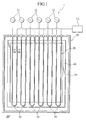
- a thin film formation apparatus is an antenna-type inductively-coupled plasma CVD apparatus, moreover, is relatively large in size to deposit on large (large area) substrates, suitable for the production of solar cells for the use in photovoltaic power generation, and is provided with a film-deposition chamber 10, array antennas 20 installed in the above film-deposition chamber 10 and substrate holders 50 to hold substrate 40 for deposition.
- the film-deposition chamber 10 is composed of the a spatial size, with enough height and width to deposit on large substrates 40, for example more than 1m square in size, and with enough depth to achieve simultaneous deposition on plural (six substrates in the illustrated example) of such substrates.
- each array antenna 20 consists of plural (six in the illustrated example) antenna elements 30.
- each antenna element 30 consists of two linear conductors, the powered conductor 31 and the grounded conductor 35, placed parallel to each other and electrically connected to adjacent ones at one end (for example at the bottom end) with a conductor 38 to form a parallel line in back and forth in almost U-shape.
- the other end of above one of the powered conductor 31 namely, the upper end
- the other end of the grounded conductor 35 namely, the upper end
- the grounding portion to be grounded.
- a solid rod is used as the powered conductor 31 and the high-frequency power feeding portion, for example, pass through a feed-through 32 made of dielectric such as Al 2 O 3 provided on the wall of film-deposition chamber 10, and is connected to a high-frequency power source 11 placed outside the film-deposition chamber 10. Furthermore, tubular dielectric pipe 33 such as Al 2 O 3 is provided around the powered conductor 31 inside the film-deposition chamber 10, and the thickness of above dielectric pipe 33 is to be suitably determined.
- a tubular pipe with many holes 36 on the surface is used as a grounded conductor 35, which upper end is grounded to the inner surface of the above film-deposition chamber 10 and is connected to a gas supply source 12 placed outside the film-deposition chamber 10. Therefore, the grounded portion of a tubular grounded conductor 35 of respective antenna element 30 functions as the source gas introduction port of the above film-deposition chamber 10.
- the above plural antenna elements 30 are arranged in such a way that each high frequency supply portion and each grounded portion, namely the powered conductors 31 and the grounded conductors 35, respectively, are alternately arranged. All powered conductors 31 and grounded conductors 35 are arranged on the same plane (hereafter, "array plane") with even intervals.
- Each array antenna 20 is constituted in such a way explained above.
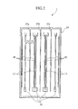
- Plural array antennas 20 three sets of array antennas, 20a, 20b and 20c in the illustrated example) are placed parallel to each other in the film-deposition chamber 10 with a prescribed intervals in between. Therefore, respective array plane is placed in the film-deposition chamber parallel to each other with a prescribed interval in between.
- the above substrate holder 50 holds a pair of substrates 40 on which thin film is to be deposited at both sides of the array antenna 20, keeping both of the substrates 40 parallel to the above array plane, and moreover, positions the distance D between the array antenna 20 and the substrates 40 (hereafter, "antenna-substrate distance D ", see Fig. 2) to be comparable (specified later) to the distance P between the powered conductors 31 and the grounded conductors 35 (see Fig. 1: for example 35mm). Since three sets of array antennas 20a, 20b and 20c are illustrated as an example, the substrate holder 50 holds one of the substrates 40 each on both sides of respective array antenna 20, resulting in six substrates 40 in total. All substrates 40 are positioned in parallel to the array plane of corresponding array antenna 20, and in such a way that the antenna-substrate distance D is set comparable to the distance P between the powered conductors 31 and the grounded conductors 35 (about 35mm).
- Such substrate holder 50 is constituted so that the substrate holder 50 can be carried in and out of the film-deposition chamber 10 supported by an appropriate carrier (not shown), in order to enable being carried in and out of the film-deposition chamber 10 while holding all of above substrates 40.
- the side plates on the left and the right sides of the film-deposition chamber 10 are designed to be capable of opening and closing, in such a way while either one of left or right (for example, left) side plate is opened and the substrate holder 50 is carried in the film-deposition chamber 10, the other one (for example, right) side plate is opened and the substrate holder 50 is carried out.
- the film-deposition chamber 10 is provided with, for example on the lower part, an exhaust port for evacuation.
- the above film-deposition chamber 10 is provided with a heat control system 13 to control the temperature of the above substrate 40 from rising during deposition.
- the heat control system 13 consists of, for example, an appropriate heat absorbent to absorb heat from the respective substrates 40 via heat radiation or heat conduction, and with a mechanism to release the heat absorbed by the absorbent to the side walls and such of the film-deposition chamber 10 by heat radiation or heat conduction.
- the heat control system 13 may be comprised of only a heat absorbent provided with a cooling function using a fluid as a medium, furthermore, without the heat absorbent and only by a waste heat function where the heat inside the film-deposition chamber 10 is forced to be released outside.
- the deposition process is performed maintaining the pressure in the above film-deposition chamber 10 at 60Pa or less.
- the above source gas is introduced inside all of the grounded conductors 35 of the respective antenna elements 30 of the array antennas 20 (20a, 20b and 20c) from the gas supply source 12 placed outside the film-deposition chamber 10.
- the source gas is introduced into the film-deposition chamber 10 through the holes 36 on the grounded conductor 35, filling the film-deposition chamber 10, and the pressure inside the film-deposition chamber 10 is controlled to be appropriate at 60Pa or less.
- the deposition process is performed by maintaining the pressure inside the film-deposition chamber 10 to be appropriate at 60Pa or less, introducing high frequency power (for example, VHF power at 85MHz) to all the powered conductors 31 of the respective antenna elements 30 of the array antennas 20 (20a, 20b and 20c) from the high-frequency power source 11 placed outside the film-deposition chamber 10, and generating plasma around all powered conductors 31 and grounded conductors 35, connected electrically by conductors 38.
- high frequency power for example, VHF power at 85MHz
- objective thin film is deposited on the surface of all (six) substrates 40 as partially shown in Fig. 4A.
- the thin film is in the form of amorphous or microcrystalline structure.
- microcrystalline silicon ( ⁇ c-Si) thin films were deposited on all (six) substrates 40 in the film-deposition chamber 10, and the film properties of the thin films were confirmed to be uniform over the whole surface of the substrates 40.
- ⁇ c-Si microcrystalline silicon
- the film-deposition chamber 10 is provided with the heat control system 13 the film properties were confirmed not being deteriorated by the temperature rise of the substrates 40 during the deposition process, due to the effect of the heat control system 1.
- Fig. 5A when the antenna-substrate distance D is about 35mm, comparable to the distance P between the powered conductors 31 and the grounded conductors 35, the signal ratio of microcrystalline silicon ( ⁇ c-Si) to amorphous silicon (a-Si) is the highest, showing good crystallinity and high quality film being obtained. It is shown that even with larger antenna-substrate distance D, up to about 47mm, considerably high quality films are obtained. Besides, the antenna-substrate distance D shorter than 35mm is not shown in Fig. 5A, however, it was confirmed that considerably high quality films are obtained down to about 17mm.
- ⁇ c-Si microcrystalline silicon
- a-Si amorphous silicon
- the optimum value of antenna-substrate distance D is about 35mm which is comparable to the distance P between the powered conductors 31 and the grounded conductors 35, and about ⁇ 50% of the above optimum value (about 17mm to about 47mm) was found to be the permissible range of the antenna-substrate distance D judging from the film quality. This supports that electromagnetic field efficiently induces ionization reaction as long as the antenna-substrate distance D is within the above permissible range.
- Fig. 4B shows the experimental results of deposition when the antenna-substrate distance D is close to the lower limit of the permissible range of the optimum value (about 35mm).
- the thickness of the deposited film on the substrates 40 is thicker at the positions corresponding to the positions of the powered conductors 31 and the grounded conductors 35, while it becomes thinner as the positions become apart from the powered conductors 31 and the grounded conductors 35, and as a result, a film with a striped pattern with thick and thin parts arranged alternately, with constant intervals corresponding to the powered conductors 31 and the grounded conductors 35, is formed on the respective substrates 40.
- the formation of above striped pattern can be avoided by repeatedly reciprocating the substrates 40 for an appropriate stroke during deposition in the direction parallel to the array plane and perpendicular to the powered conductors 31 and grounded conductors 35.
- the length of reciprocating stroke S is, as shown in Fig. 4C, preferably about twice the distance P (about 35mm) between the powered conductors 31 and the grounded conductors 35 (S ⁇ 2P), that is to say, corresponding to the distance between adjacent array elements 30 of the array antenna 20 (70mm).
- the antenna-substrate distance D is set to a value, within the permissible range and near the optimum value, where the optimum value is comparable to the distance between the powered conductors 31 and the grounded conductors 35 (about 35mm) and the permissible range is about ⁇ 50% of the optimum value.
- the antenna-substrate distance D is apart from the optimum value, as long as it is set within the permissible range, it was confirmed to be able to form high quality microcrystalline film uniformly without a striped pattern by repeatedly reciprocating the substrates 40 for appropriate stroke during deposition.
- the deposition rate shows a maximum value when the antenna-substrate distance D is about 40mm, and becomes lower when the antenna- substrate distance D is longer or shorter than this value.
- the deposition rate shows the maximum value when the antenna-substrate distance D is about 40mm as shown in Fig. 5B, that is longer than the optimum value for film quality which is about 35mm.
- One of the reasons for this is suggested to be due to the electromagnetic field, generated around the above powered conductors 31 and the grounded conductors 35 of above array antenna 20, pass through the substrates 40 or leak out when the substrate 40 is too close to the array antenna 20.
- metal backing-plates at the back sides of the substrates 40. This is because VHF power can be made efficiently absorbed into plasma as the metal backing-plates reflect the electromagnetic field.
- the optimum value for antenna-substrate distance D was about 35mm, and the permissible range was between about 17mm and about 47mm, however, if the distance P between the powered conductors 31 and the grounded conductors 35 is other than this value, as a matter of course, the optimum value of the antenna-substrate distance D depends on the above value, and the permissible range becomes about ⁇ 50% of the above antenna-substrate distance D.
- the thin film formation apparatus 1 (antenna-type inductively-coupled plasma CVD apparatus) for deposition, simultaneous deposition of thin films on the surface of two substrates 40 per one set of array antenna 20, one substrate per one side of array antenna 20, can be performed.
- the thin film formation apparatus 1 is provided with three sets of array antennas 20a, 20b and 20c, simultaneous deposition of thin films on the surface of two substrates per each array antenna 20, total of six of substrates 20 can be carried out.
- the above respective array antenna 20 is composed of plural antenna elements 30, where the number of antenna elements 30 (six in the example shown in figures) can be increased to any number in principle up to the limitation of the dimension of the film-deposition chamber 10. Therefore, there is no principle limit in size in the width direction in Fig. 1 in order to increase the size of respective substrates 40.
- the length of the powered conductors 31 and the grounded conductors 35 of respective antenna elements 30 has to be elongated in order to increase the size of respective substrates 40 in the height direction in Fig. 1.
- the dielectric pipe 33 provided around the powered conductors 31 is effective to elongate the length of the powered conductors 31 and the grounded conductors 35.
- plasma is only generated for a short distance form the upper part.
- the plasma density can be maintained uniform.
- this method can be used to control the crystallinity and deposition rate of thin films to be obtained.
- the impedance cannot be matched due to the relation between the dielectric constant of the plasma and the shape of the antenna, it is possible to make the impedance matched by, for example, controlling the dielectric constant of the feed-through by changing the thickness of its dielectric, or by adding an appropriate impedance element to the ends of above powered conductors 31 and grounded conductors 35 of respective antenna elements 30 or to the conductors 38.
- the thin film formation apparatus 1 can be utilized as a thin film formation apparatus which is capable to deposit high quality a-Si thin film with uniform thickness distribution on large substrates.
- a-Si thin film is suitable for the use in solar cells, therefore, the above thin film formation apparatus 1 is suitable to be utilized as solar cell production apparatus.
- the above thin film formation apparatus 1 can be utilized as the thin film formation apparatus for the formation of tandem structure solar cells.
- the number of the film-deposition chamber 10 was explained and illustrated as being one, however, the number is not limited to this.
- plural plasma sources can be arranged in a limited space with substrates facing to them, and uniform plasma can be generated between respective plasma sources and the substrates, simultaneous deposition on a number of substrates with uniform properties and thickness distribution can be performed, enabling efficient production of thin films.
Landscapes
- Chemical & Material Sciences (AREA)
- Engineering & Computer Science (AREA)
- Materials Engineering (AREA)
- Plasma & Fusion (AREA)
- General Chemical & Material Sciences (AREA)
- Chemical Kinetics & Catalysis (AREA)
- Physics & Mathematics (AREA)
- Mechanical Engineering (AREA)
- Metallurgy (AREA)
- Organic Chemistry (AREA)
- Chemical Vapour Deposition (AREA)
- Plasma Technology (AREA)
- Photovoltaic Devices (AREA)
- Variable-Direction Aerials And Aerial Arrays (AREA)
Applications Claiming Priority (3)
| Application Number | Priority Date | Filing Date | Title |
|---|---|---|---|
| JP2002292948 | 2002-10-04 | ||
| JP2002292948 | 2002-10-04 | ||
| PCT/JP2003/012722 WO2004031443A1 (ja) | 2002-10-04 | 2003-10-03 | 薄膜形成方法およびその装置 |
Publications (3)
| Publication Number | Publication Date |
|---|---|
| EP1548151A1 true EP1548151A1 (de) | 2005-06-29 |
| EP1548151A4 EP1548151A4 (de) | 2009-05-20 |
| EP1548151B1 EP1548151B1 (de) | 2014-04-23 |
Family
ID=32063936
Family Applications (1)
| Application Number | Title | Priority Date | Filing Date |
|---|---|---|---|
| EP03751327.2A Expired - Lifetime EP1548151B1 (de) | 2002-10-04 | 2003-10-03 | Verfahren zur herstellung von dünnem film und vorrichtung dafür |
Country Status (9)
| Country | Link |
|---|---|
| US (2) | US8034418B2 (de) |
| EP (1) | EP1548151B1 (de) |
| JP (2) | JP4120546B2 (de) |
| KR (2) | KR20050053729A (de) |
| CN (1) | CN100462477C (de) |
| AU (1) | AU2003271089B2 (de) |
| CA (1) | CA2500898C (de) |
| TW (1) | TWI275662B (de) |
| WO (1) | WO2004031443A1 (de) |
Cited By (2)
| Publication number | Priority date | Publication date | Assignee | Title |
|---|---|---|---|---|
| WO2012119700A1 (de) * | 2011-03-09 | 2012-09-13 | Manz Ag | Vorrichtung und verfahren zum plasmaunterstützten behandeln zumindest zweier substrate |
| EP2544223A4 (de) * | 2010-03-03 | 2013-08-14 | Mitsui Shipbuilding Eng | Dünnschichtbildende vorrichtung |
Families Citing this family (28)
| Publication number | Priority date | Publication date | Assignee | Title |
|---|---|---|---|---|
| US20060120213A1 (en) * | 2004-11-17 | 2006-06-08 | Tonkovich Anna L | Emulsion process using microchannel process technology |
| JP2006237469A (ja) * | 2005-02-28 | 2006-09-07 | Toray Eng Co Ltd | プラズマcvd装置及びプラズマcvd方法 |
| US8251012B2 (en) * | 2005-03-01 | 2012-08-28 | Hitachi Kokusai Electric Inc. | Substrate processing apparatus and semiconductor device producing method |
| JP5309426B2 (ja) * | 2006-03-29 | 2013-10-09 | 株式会社Ihi | 微結晶シリコン膜形成方法及び太陽電池 |
| KR101354253B1 (ko) * | 2007-02-15 | 2014-01-22 | 어플라이드 머티어리얼스, 인코포레이티드 | 평면 및 3차원의 pecvd 코팅에 있어서의 국부화된 부분 압력을 제어하기 위한 국부화된 선형 마이크로파 소스 어레이 펌핑 |
| JP2010519408A (ja) * | 2007-02-15 | 2010-06-03 | アプライド マテリアルズ インコーポレイテッド | 化学気相堆積プロセスを制御するシステム及び方法 |
| WO2010058560A1 (ja) * | 2008-11-20 | 2010-05-27 | 株式会社エバテック | プラズマ処理装置 |
| TWI521088B (zh) * | 2009-10-28 | 2016-02-11 | 應用材料股份有限公司 | 用於處理多個基材的製程腔室與用於在基材上沉積膜的製程 |
| EP2564425B1 (de) | 2010-04-28 | 2019-05-29 | Nokia Technologies Oy | Anordnung aus pv-zellen |
| WO2011137371A2 (en) * | 2010-04-30 | 2011-11-03 | Applied Materials, Inc. | Vertical inline cvd system |
| JP5609661B2 (ja) * | 2011-01-17 | 2014-10-22 | 株式会社Ihi | 誘導結合型の二重管電極及びアレイアンテナ式のcvdプラズマ装置 |
| JP5699644B2 (ja) * | 2011-01-31 | 2015-04-15 | 株式会社Ihi | アンテナ搬送体、アレイアンテナ式プラズマcvd装置、並びに、アレイアンテナ式プラズマcvd装置のアレイアンテナユニット取り付け方法 |
| JP5582050B2 (ja) * | 2011-01-31 | 2014-09-03 | 株式会社Ihi | アンテナ搬送体およびアレイアンテナ式プラズマcvd装置 |
| JP5780023B2 (ja) * | 2011-07-07 | 2015-09-16 | 株式会社Ihi | プラズマcvd装置およびプラズマcvd装置を用いた成膜方法 |
| JP2013044044A (ja) * | 2011-08-26 | 2013-03-04 | Ihi Corp | アレイアンテナ式のcvdプラズマ装置 |
| US20140210337A1 (en) * | 2011-08-30 | 2014-07-31 | Emd Corporation | Antenna for plasma processing device, and plasma processing device using the same |
| GB2489761B (en) * | 2011-09-07 | 2015-03-04 | Europlasma Nv | Surface coatings |
| JP5757469B2 (ja) * | 2011-10-13 | 2015-07-29 | 株式会社Ihi | アレイアンテナ式のcvdプラズマ装置 |
| JP5617817B2 (ja) | 2011-10-27 | 2014-11-05 | パナソニック株式会社 | 誘導結合型プラズマ処理装置及び誘導結合型プラズマ処理方法 |
| WO2013122954A1 (en) * | 2012-02-13 | 2013-08-22 | Applied Materials, Inc. | Linear pecvd apparatus |
| JP6010981B2 (ja) * | 2012-04-03 | 2016-10-19 | 株式会社Ihi | プラズマ処理装置 |
| JP2013214445A (ja) * | 2012-04-03 | 2013-10-17 | Ihi Corp | プラズマ処理装置 |
| KR101379701B1 (ko) * | 2012-11-28 | 2014-04-01 | 한국표준과학연구원 | 기판 처리 장치 및 기판 처리 방법 |
| JP2014109060A (ja) * | 2012-12-03 | 2014-06-12 | Ihi Corp | アレイアンテナ式のcvdプラズマ装置 |
| JP5482937B2 (ja) * | 2013-05-13 | 2014-05-07 | 株式会社Ihi | 太陽電池の製造方法 |
| JP6656656B2 (ja) * | 2015-10-02 | 2020-03-04 | 株式会社Ihi | 触媒の製造装置 |
| CN106571407B (zh) * | 2016-10-11 | 2017-10-13 | 南京奥依菲光电科技有限公司 | 具有聚拢太阳能特性的微纳米天线太阳能电池及工作方法 |
| WO2020023874A1 (en) * | 2018-07-26 | 2020-01-30 | Lam Research Corporation | Compact high density plasma source |
Family Cites Families (21)
| Publication number | Priority date | Publication date | Assignee | Title |
|---|---|---|---|---|
| US3907660A (en) * | 1970-07-31 | 1975-09-23 | Ppg Industries Inc | Apparatus for coating glass |
| JPS5914633A (ja) | 1982-07-16 | 1984-01-25 | Anelva Corp | プラズマcvd装置 |
| US4664951A (en) * | 1985-07-31 | 1987-05-12 | Energy Conversion Devices, Inc. | Method provided for corrective lateral displacement of a longitudinally moving web held in a planar configuration |
| US4801474A (en) * | 1986-01-14 | 1989-01-31 | Canon Kabushiki Kaisha | Method for forming thin film multi-layer structure member |
| US5082696A (en) * | 1986-10-03 | 1992-01-21 | Dow Corning Corporation | Method of forming semiconducting amorphous silicon films from the thermal decomposition of dihalosilanes |
| JPH07118464B2 (ja) * | 1988-02-12 | 1995-12-18 | 株式会社島津製作所 | プラズマ付着装置 |
| JPH06248461A (ja) | 1993-02-26 | 1994-09-06 | Hitachi Zosen Corp | プラズマcvd装置 |
| US5456763A (en) * | 1994-03-29 | 1995-10-10 | The Regents Of The University Of California | Solar cells utilizing pulsed-energy crystallized microcrystalline/polycrystalline silicon |
| TW320687B (de) * | 1996-04-01 | 1997-11-21 | Toray Industries | |
| JPH11135438A (ja) * | 1997-10-28 | 1999-05-21 | Nippon Asm Kk | 半導体プラズマ処理装置 |
| DE29821644U1 (de) * | 1998-12-04 | 1999-02-18 | Stocko Metallwarenfab Henkels | Authentifikationssystem für PC-Cards |
| JP2000345351A (ja) * | 1999-05-31 | 2000-12-12 | Anelva Corp | プラズマcvd装置 |
| DE19935046C2 (de) * | 1999-07-26 | 2001-07-12 | Schott Glas | Plasma-CVD-Verfahren und Vorrichtung zur Herstellung einer mikrokristallinen Si:H-Schicht auf einem Substrat sowie deren Verwendung |
| DE60045574D1 (de) | 1999-09-09 | 2011-03-10 | Ihi Corp | Plasmabehandlungsvorrichtung mit innenelktrode und plasmabehandlungsverfahren |
| JP4462461B2 (ja) | 2000-04-13 | 2010-05-12 | 株式会社Ihi | 薄膜形成方法、薄膜形成装置及び太陽電池 |
| JP4509337B2 (ja) * | 2000-09-04 | 2010-07-21 | 株式会社Ihi | 薄膜形成方法及び薄膜形成装置 |
| DE60134081D1 (de) * | 2000-04-13 | 2008-07-03 | Ihi Corp | Herstellungsverfahren von Dünnschichten, Gerät zur Herstellung von Dünnschichten und Sonnenzelle |
| KR100797423B1 (ko) * | 2000-05-17 | 2008-01-23 | 가부시키가이샤 아이에이치아이 | 플라즈마 cvd 장치 및 방법 |
| JP2001332749A (ja) * | 2000-05-23 | 2001-11-30 | Canon Inc | 半導体薄膜の形成方法およびアモルファスシリコン太陽電池素子 |
| JP4770029B2 (ja) * | 2001-01-22 | 2011-09-07 | 株式会社Ihi | プラズマcvd装置及び太陽電池の製造方法 |
| JP2002246619A (ja) | 2001-02-13 | 2002-08-30 | Kanegafuchi Chem Ind Co Ltd | 薄膜光電変換装置の製造方法 |
-
2003
- 2003-09-25 JP JP2003333037A patent/JP4120546B2/ja not_active Expired - Fee Related
- 2003-10-03 CA CA2500898A patent/CA2500898C/en not_active Expired - Fee Related
- 2003-10-03 TW TW092127496A patent/TWI275662B/zh not_active IP Right Cessation
- 2003-10-03 US US10/529,904 patent/US8034418B2/en not_active Expired - Fee Related
- 2003-10-03 AU AU2003271089A patent/AU2003271089B2/en not_active Ceased
- 2003-10-03 WO PCT/JP2003/012722 patent/WO2004031443A1/ja not_active Ceased
- 2003-10-03 KR KR1020057005743A patent/KR20050053729A/ko not_active Ceased
- 2003-10-03 KR KR1020117000788A patent/KR101096554B1/ko not_active Expired - Fee Related
- 2003-10-03 CN CNB2003801008848A patent/CN100462477C/zh not_active Expired - Fee Related
- 2003-10-03 EP EP03751327.2A patent/EP1548151B1/de not_active Expired - Lifetime
-
2007
- 2007-10-19 JP JP2007273021A patent/JP2008106362A/ja active Pending
-
2011
- 2011-08-17 US US13/211,901 patent/US20110297089A1/en not_active Abandoned
Non-Patent Citations (2)
| Title |
|---|
| No further relevant documents disclosed * |
| See also references of WO2004031443A1 * |
Cited By (2)
| Publication number | Priority date | Publication date | Assignee | Title |
|---|---|---|---|---|
| EP2544223A4 (de) * | 2010-03-03 | 2013-08-14 | Mitsui Shipbuilding Eng | Dünnschichtbildende vorrichtung |
| WO2012119700A1 (de) * | 2011-03-09 | 2012-09-13 | Manz Ag | Vorrichtung und verfahren zum plasmaunterstützten behandeln zumindest zweier substrate |
Also Published As
| Publication number | Publication date |
|---|---|
| US20060011231A1 (en) | 2006-01-19 |
| KR20050053729A (ko) | 2005-06-08 |
| US8034418B2 (en) | 2011-10-11 |
| EP1548151B1 (de) | 2014-04-23 |
| CN1703533A (zh) | 2005-11-30 |
| EP1548151A4 (de) | 2009-05-20 |
| AU2003271089B2 (en) | 2009-03-19 |
| WO2004031443A1 (ja) | 2004-04-15 |
| JP4120546B2 (ja) | 2008-07-16 |
| JP2008106362A (ja) | 2008-05-08 |
| US20110297089A1 (en) | 2011-12-08 |
| TWI275662B (en) | 2007-03-11 |
| KR101096554B1 (ko) | 2011-12-20 |
| AU2003271089A1 (en) | 2004-04-23 |
| KR20110018942A (ko) | 2011-02-24 |
| CN100462477C (zh) | 2009-02-18 |
| CA2500898A1 (en) | 2004-04-15 |
| TW200413563A (en) | 2004-08-01 |
| CA2500898C (en) | 2011-01-25 |
| JP2004143592A (ja) | 2004-05-20 |
Similar Documents
| Publication | Publication Date | Title |
|---|---|---|
| US8034418B2 (en) | Method for forming thin film and apparatus therefor | |
| US6719876B1 (en) | Internal electrode type plasma processing apparatus and plasma processing method | |
| EP2009140B1 (de) | Verfahren zur bildung eines films aus mirkokristallinem silicium | |
| US20100144122A1 (en) | Hybrid chemical vapor deposition process combining hot-wire cvd and plasma-enhanced cvd | |
| KR20100034737A (ko) | 균일한 실리콘 필름을 증착하기 위한 장치 및 균일한 실리콘 필름을 제조하기 위한 방법 | |
| WO2009133189A1 (en) | Plasma processing apparatus and method for the plasma processing of substrates | |
| CN101882647A (zh) | 一种硅基薄膜太阳能电池活动夹具 | |
| KR20090101166A (ko) | 전자 사이클로트론 공진에 의해 구배화된 밴드갭을 가진 비정질 막들의 막 증착 | |
| JP4859472B2 (ja) | プラズマプロセス装置 | |
| JP4279217B2 (ja) | プラズマ処理装置及びこれを用いた太陽電池の製造方法 | |
| CN116516321B (zh) | 一种箱式可扩展堆栈pecvd系统 | |
| KR20110036932A (ko) | 기판 상에 처리되는 물질의 균일성 개선을 위한 증착 장치 및 그 사용 방법 | |
| EP0848434A2 (de) | Herstellungsverfahren für Halbleiter-Dünnschichten | |
| KR20110074854A (ko) | 유량 경사 설계를 갖는 균일한 실리콘 막을 증착하는 방법 및 장치 | |
| JP3144165B2 (ja) | 薄膜生成装置 | |
| JPS6239532B2 (de) | ||
| EP1122337A2 (de) | Vorrichting und Verfahren zum Abscheiden eines Films | |
| Takagi et al. | Large area multi-zone type VHF-PCVD system for a-Si and/spl mu/c-Si deposition | |
| JP2000355771A (ja) | 堆積膜形成方法および堆積膜形成装置 | |
| HU227809B1 (hu) | Eljárás és berendezés félvezető vékonyréteg több hordozón egyidejűleg történő előállítására | |
| CN201780981U (zh) | 太阳能电池活动夹具 | |
| JP2000164518A (ja) | 半導体堆積膜の形成方法及びその形成装置 |
Legal Events
| Date | Code | Title | Description |
|---|---|---|---|
| PUAI | Public reference made under article 153(3) epc to a published international application that has entered the european phase |
Free format text: ORIGINAL CODE: 0009012 |
|
| 17P | Request for examination filed |
Effective date: 20050414 |
|
| AK | Designated contracting states |
Kind code of ref document: A1 Designated state(s): AT BE BG CH CY CZ DE DK EE ES FI FR GB GR HU IE IT LI LU MC NL PT RO SE SI SK TR |
|
| AX | Request for extension of the european patent |
Extension state: AL LT LV MK |
|
| DAX | Request for extension of the european patent (deleted) | ||
| RBV | Designated contracting states (corrected) |
Designated state(s): CH DE LI NL |
|
| RAP1 | Party data changed (applicant data changed or rights of an application transferred) |
Owner name: IHI CORPORATION |
|
| A4 | Supplementary search report drawn up and despatched |
Effective date: 20090421 |
|
| 17Q | First examination report despatched |
Effective date: 20110412 |
|
| GRAP | Despatch of communication of intention to grant a patent |
Free format text: ORIGINAL CODE: EPIDOSNIGR1 |
|
| INTG | Intention to grant announced |
Effective date: 20131119 |
|
| GRAS | Grant fee paid |
Free format text: ORIGINAL CODE: EPIDOSNIGR3 |
|
| GRAA | (expected) grant |
Free format text: ORIGINAL CODE: 0009210 |
|
| AK | Designated contracting states |
Kind code of ref document: B1 Designated state(s): CH DE LI NL |
|
| REG | Reference to a national code |
Ref country code: CH Ref legal event code: EP |
|
| REG | Reference to a national code |
Ref country code: DE Ref legal event code: R082 Ref document number: 60346051 Country of ref document: DE Representative=s name: MARKS & CLERK (LUXEMBOURG) LLP, LU |
|
| REG | Reference to a national code |
Ref country code: DE Ref legal event code: R096 Ref document number: 60346051 Country of ref document: DE Effective date: 20140528 |
|
| REG | Reference to a national code |
Ref country code: CH Ref legal event code: NV Representative=s name: MARKS AND CLERK (LUXEMBOURG) LLP, CH |
|
| REG | Reference to a national code |
Ref country code: NL Ref legal event code: T3 |
|
| REG | Reference to a national code |
Ref country code: DE Ref legal event code: R097 Ref document number: 60346051 Country of ref document: DE |
|
| PLBE | No opposition filed within time limit |
Free format text: ORIGINAL CODE: 0009261 |
|
| STAA | Information on the status of an ep patent application or granted ep patent |
Free format text: STATUS: NO OPPOSITION FILED WITHIN TIME LIMIT |
|
| 26N | No opposition filed |
Effective date: 20150126 |
|
| REG | Reference to a national code |
Ref country code: DE Ref legal event code: R097 Ref document number: 60346051 Country of ref document: DE Effective date: 20150126 |
|
| PGFP | Annual fee paid to national office [announced via postgrant information from national office to epo] |
Ref country code: NL Payment date: 20200915 Year of fee payment: 18 |
|
| PGFP | Annual fee paid to national office [announced via postgrant information from national office to epo] |
Ref country code: DE Payment date: 20200922 Year of fee payment: 18 Ref country code: CH Payment date: 20201015 Year of fee payment: 18 |
|
| REG | Reference to a national code |
Ref country code: DE Ref legal event code: R119 Ref document number: 60346051 Country of ref document: DE |
|
| REG | Reference to a national code |
Ref country code: CH Ref legal event code: PL |
|
| REG | Reference to a national code |
Ref country code: NL Ref legal event code: MM Effective date: 20211101 |
|
| PG25 | Lapsed in a contracting state [announced via postgrant information from national office to epo] |
Ref country code: NL Free format text: LAPSE BECAUSE OF NON-PAYMENT OF DUE FEES Effective date: 20211101 Ref country code: DE Free format text: LAPSE BECAUSE OF NON-PAYMENT OF DUE FEES Effective date: 20220503 |
|
| PG25 | Lapsed in a contracting state [announced via postgrant information from national office to epo] |
Ref country code: LI Free format text: LAPSE BECAUSE OF NON-PAYMENT OF DUE FEES Effective date: 20211031 Ref country code: CH Free format text: LAPSE BECAUSE OF NON-PAYMENT OF DUE FEES Effective date: 20211031 |