EP1547294B1 - Procede et appareil d'analyse de taux d'erreur binaire - Google Patents
Procede et appareil d'analyse de taux d'erreur binaire Download PDFInfo
- Publication number
- EP1547294B1 EP1547294B1 EP03754944A EP03754944A EP1547294B1 EP 1547294 B1 EP1547294 B1 EP 1547294B1 EP 03754944 A EP03754944 A EP 03754944A EP 03754944 A EP03754944 A EP 03754944A EP 1547294 B1 EP1547294 B1 EP 1547294B1
- Authority
- EP
- European Patent Office
- Prior art keywords
- threshold
- data signal
- bit
- bit error
- clock
- Prior art date
- Legal status (The legal status is an assumption and is not a legal conclusion. Google has not performed a legal analysis and makes no representation as to the accuracy of the status listed.)
- Expired - Lifetime
Links
- 238000000034 method Methods 0.000 title claims abstract description 29
- 238000012360 testing method Methods 0.000 claims abstract description 20
- 230000000737 periodic effect Effects 0.000 claims description 12
- 238000011084 recovery Methods 0.000 claims description 11
- 238000012545 processing Methods 0.000 claims description 7
- 230000001360 synchronised effect Effects 0.000 abstract description 5
- 230000007704 transition Effects 0.000 description 15
- 238000005259 measurement Methods 0.000 description 8
- 238000010586 diagram Methods 0.000 description 7
- 238000006243 chemical reaction Methods 0.000 description 4
- 230000006870 function Effects 0.000 description 3
- 230000004044 response Effects 0.000 description 3
- 238000005070 sampling Methods 0.000 description 3
- 230000001143 conditioned effect Effects 0.000 description 2
- 238000010276 construction Methods 0.000 description 2
- RGNPBRKPHBKNKX-UHFFFAOYSA-N hexaflumuron Chemical compound C1=C(Cl)C(OC(F)(F)C(F)F)=C(Cl)C=C1NC(=O)NC(=O)C1=C(F)C=CC=C1F RGNPBRKPHBKNKX-UHFFFAOYSA-N 0.000 description 2
- 230000008569 process Effects 0.000 description 2
- 230000035945 sensitivity Effects 0.000 description 2
- 101150071746 Pbsn gene Proteins 0.000 description 1
- 238000004364 calculation method Methods 0.000 description 1
- 230000008859 change Effects 0.000 description 1
- 230000003750 conditioning effect Effects 0.000 description 1
- 238000012937 correction Methods 0.000 description 1
- 230000002596 correlated effect Effects 0.000 description 1
- 230000000875 corresponding effect Effects 0.000 description 1
- 230000001419 dependent effect Effects 0.000 description 1
- 230000000694 effects Effects 0.000 description 1
- 230000007613 environmental effect Effects 0.000 description 1
- 230000003252 repetitive effect Effects 0.000 description 1
- 238000010845 search algorithm Methods 0.000 description 1
Images




Classifications
-
- H—ELECTRICITY
- H04—ELECTRIC COMMUNICATION TECHNIQUE
- H04L—TRANSMISSION OF DIGITAL INFORMATION, e.g. TELEGRAPHIC COMMUNICATION
- H04L1/00—Arrangements for detecting or preventing errors in the information received
- H04L1/24—Testing correct operation
- H04L1/242—Testing correct operation by comparing a transmitted test signal with a locally generated replica
-
- H—ELECTRICITY
- H04—ELECTRIC COMMUNICATION TECHNIQUE
- H04L—TRANSMISSION OF DIGITAL INFORMATION, e.g. TELEGRAPHIC COMMUNICATION
- H04L1/00—Arrangements for detecting or preventing errors in the information received
- H04L1/20—Arrangements for detecting or preventing errors in the information received using signal quality detector
- H04L1/203—Details of error rate determination, e.g. BER, FER or WER
-
- H—ELECTRICITY
- H04—ELECTRIC COMMUNICATION TECHNIQUE
- H04L—TRANSMISSION OF DIGITAL INFORMATION, e.g. TELEGRAPHIC COMMUNICATION
- H04L7/00—Arrangements for synchronising receiver with transmitter
- H04L7/0016—Arrangements for synchronising receiver with transmitter correction of synchronization errors
- H04L7/002—Arrangements for synchronising receiver with transmitter correction of synchronization errors correction by interpolation
- H04L7/0029—Arrangements for synchronising receiver with transmitter correction of synchronization errors correction by interpolation interpolation of received data signal
-
- H—ELECTRICITY
- H04—ELECTRIC COMMUNICATION TECHNIQUE
- H04L—TRANSMISSION OF DIGITAL INFORMATION, e.g. TELEGRAPHIC COMMUNICATION
- H04L7/00—Arrangements for synchronising receiver with transmitter
- H04L7/02—Speed or phase control by the received code signals, the signals containing no special synchronisation information
- H04L7/033—Speed or phase control by the received code signals, the signals containing no special synchronisation information using the transitions of the received signal to control the phase of the synchronising-signal-generating means, e.g. using a phase-locked loop
- H04L7/0334—Processing of samples having at least three levels, e.g. soft decisions
Definitions
- the present invention relates to a method of bit error rate analysis for signals sampled in a digital oscilloscope.
- Bit error rate measurement is central to all serial data testing. All other measurements relate back to this one parameter which is the ultimate measurement of link quality. Oscilloscopes in general have typically measured bit error rates from an eye diagram or from a jitter bathtub curve. However, in very high sample acquisitions, these methods have proved unacceptable. US-A-3562710 (Halleck ) discloses a bit error detector that compares a received signal with a reference to determine the bit error rate.
- the LeCroy® SDA computes a bit error rate by first collecting a long waveform acquisition of a bit pattern. Using a recovered periodic clock, the waveform is sampled at an optimum threshold level and the resulting sequence of bits is stored and compared with a known bit pattern.
- This bit pattern may be a standard pattern, a pseudo-randomly generated pattern, or a custom pattern.
- An automatic search algorithm is provided which aligns the known and measured patterns.
- bit error rate be measured directly in software by using a software recovered clock to define a plurality of data segments, converting the data segments of the captured waveform to bits, which are then compared with a known data pattern.
- Bit Error Rate measures the actual bit error rate of a particular received signal using appropriate software. The following measurements can be computed:
- the software BER mode described in accordance with the invention enables the instrument to display error locations within the data stream, as is noted below.
- the minimum bit error rate can be reduced by the use of multiple data acquisitions, if it is assumed that the errors are random and stationary i.e. they are not correlated in time.
- the invention accordingly comprises the several steps and the relation of one or more of such steps with respect to each of the others, and the apparatus embodying features of construction, combination(s) of elements and arrangement of parts that are adapted to effect such steps, all as exemplified in the following detailed disclosure, and the scope of the invention will be indicated in the claims.
- an actual bit error map such as that shown at 225, is displayed to a user. Errors show up as a different color (white in the figure). Random errors show up as random spots, while any type of repetitive errors will be shown as a pattern, the particular pattern being indicative of the type of error.
- a representation of what this actual bit error map looks like is shown at display 205, and includes a 3-dimensional plot, where bit errors 220 are located within the input data stream.
- a display 205 divides the data stream into a row-column format 215 with the rows containing all of the bits 210 in a frame. A data frame is delimited either by a specific bit sequence (i.e.
- 0xF268 for SONET/SDH that is user-selectable or a fixed number of bits.
- This display depicts frame-related error sources as vertical streaks, with the horizontal dimension being bit number and the vertical dimension being frame number. The location of a bit error will be displayed as a contrasting color on an x-y display.
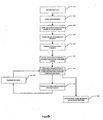
- FIG. 3 shows the steps necessary to generate the bit error location map, these steps being described below.
- FIG. 7 is a flowchart diagram depicting the procedure for analyzing an acquired and stored waveform and generating a recovered virtual periodic clock associated with the stored waveform.
- an acquired, stored data signal is retrieved from memory.
- step 115 in order to analyze the data signal for threshold crossings to subsequently define a series of "samples" acquired at nearly uniform sample-intervals, either an absolute or a relative (percentage of the recorded waveform's amplitude) vertical threshold is defined.
- each portion of the data signal is compared with the threshold to locate pairs of adjacent samples of the data signal that straddle or span the threshold. That is, one sample is greater-than-or-equal-to the threshold and the adjacent sample is less-than-or-equal-to the threshold. Hysteresis requirements must also be taken into account before an identified sample pair can be accepted as a true independent threshold crossing point, thus eliminating local noise that would contribute to jitter. Thereafter, using either linear or non-linear interpolation, an estimate of the time of crossing through the threshold that is more precise than the sample interval is made at step 125. This defines an observed time of threshold crossing. At step 127, the phase of the virtual clock is initialized.
- the initial phase is set equal to the time of threshold crossing of the first observed transition. (i.e. the first observed crossing time serving as an estimate of the recovered clock's initial phase).
- the initial phase must be further refined by one of several methods: either 1) the first N transitions in the data are discarded or 2) after some number, N transitions have been detected, the initial phase of the virtual clock is revised to give a mean time-error for these N transitions of zero, then processing is restarted. Both methods address the issue of PLL start-up or PLL acquisition time. The second of these procedures is appropriate to the case where it is desired to make the recovered clock perfectly periodic rather than tracking low frequency variations of the input data stream.
- the observed times of threshold crossing are compared to an expected time of threshold crossing at step 130.
- the expected times of threshold crossing correspond to the regular intervals of an entirely conceptual or virtual "periodic clock" that is intended to correspond, after correction as noted below, to the sequence of expected times of threshold crossing.
- phase of the recovered clock is then adjusted to properly synchronize with the observed times of threshold crossing in the recorded data signal in step 135.
- the amount of phase adjustment in each bit interval is determined by mathematical algorithms precisely defining the dynamic response of the software PLL.
- the dynamic response of the PLL can be matched to the communications standard associated with the data signal under analysis under software control.
- the recorded waveform under analysis is not necessarily of a clock but rather of a data stream presumably generated in accordance with a clock, a transition will not occur for each bit interval. That is, some transitions in the actual data signal may not be present because some consecutive bit locations may have the same value (consecutive logic "1", for example), and therefore not have a transition between them. It is possible to determine how many of these bit locations do not have transitions by assuming that the observed transitions have a correspondence with the closest expected transition of the generated virtual clock. As such, it is possible to associate every transition observed with a virtual clock transition, and to know exactly how many cycles of the generated virtual clock have passed since the previous observed transition.
- phase error time interval error "TIE" between the expected value of a threshold crossing time determined in accordance with the recovered virtual periodic clock and the actual observed value of the threshold crossing time
- TIE time interval error
- step 140 this generated error feedback signal is fed back and used at step 135 to adjust the phase of the expected time of threshold crossing. This procedure is repeated and continued until all the expected values of threshold crossing times, and therefore phase of the recovered virtual clock is locked to the actual observed values of the threshold crossing times.
- the implementation is in software; the expected times being calculated by adding floating-point numbers rather than using resonating circuits, but the result being quite similar.
- the result is also more repeatable than the analog counterpart because the functionality does not depend on manufactured components that have initial inaccuracies and change over time and varying environmental conditions, but rather is a mathematical calculation. Thus, any additional jitter generated in accordance with physical generation of a clock signal is avoided.
- this expected value of a threshold crossing time can be used to derive the ideal "sampling times" of the digitally encoded signal in the recorded waveform, as is shown in step 150. These times are between the expected times of threshold crossing (when that data is NOT changing, rather than when it is changing). Having determined these expected values of time of threshold crossing, and thus ideal sampling times, the recorded waveform can be decoded according to these ideal sampling times (recovered periodic clock) to determine bit states of the data during each "slice" of the data signal.
- Each slice of data is therefore obtained from a recorded signal of many bit transitions and by using the clock recovery system in accordance with the invention.
- the waveform of the data signal can therefore be sliced up and represented as a series of smaller waveforms (each derived from the original) but which span some number of bits from the original data signal in a precisely prescribed period of time.
- a "slicer" serves the purpose of supplying such waveforms each of which is a subset of the waveform of the input data signal, and that are synchronized with the recovered clock (extracted from the same waveform), and for which the state of the bits in each slice are (or can be) known.
- an oscilloscope As displayed on an oscilloscope, it supplies waveforms with an effective trigger time corresponding to, for example, the first division (of ten) and an end of one bit interval (unit-interval) at the 9th division on the oscilloscope display, although other timing sequences may be employed as desired. As such these waveforms are ideal for further processing as they are precisely synchronized and in phase with the recovered virtual clock.
- an analog to digital conversion (A/D) procedure receives the recovered clock from step 315, and received the acquired waveform from step 310.
- the procedure at step 320 is more completely described making reference to figure 4 .
- the analog waveform is sampled and a digital bit is produced. If the analog value at the center of the recovered clock period is greater than or equal to a threshold level, the data is said to be a digital ⁇ 1'. If it is less than the threshold, it is said to be a digital '0'.
- This procedure is applied to all portions of a waveform, in accordance with the recovered clock, to generate the digital data signal.
- step 325 the procedure for synchronizing a frame or frameless data to be tested with a test sequence is undertaken.
- an inquiry is made as to whether a frame synchronization is specified. If this inquiry is answered in the affirmative, at step 330 the bit stream provided by the analog to digital converter is divided into frames either by synchronizing to the specified header and/or by the number of bits. Once designated, the frame data designated bits of the reference signal are forwarded to step 335 for pattern synchronization. A sync indicator is also forwarded directly to an error map generating step 350 for generating the map shown in figure 2 . Thus, if a frame is defined, the display map, and pattern synchronization are performed frame by frame.
- step 325 the digital data is forwarded directly to step 335 where the generated digital data segments are compared to one of a plurality of predetermined patterns.
- predetermined patterns may comprise one of a standard pattern, pseudo-randomly generated pattern, or custom pattern stored in a data file.
- step 340 the bits of the data segments are compared to the designated pattern generated in step 335. During these comparisons, Bit Error Rate statistics are accumulated at step 345. Then at step 350, the Bit Error Map of figure 2 is generated.
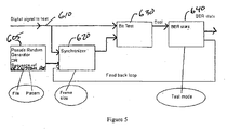
- step 335 The process of synchronization of frame data, if present, as described in step 335, and the comparison of the frame data or frameless data and either the standard pattern, the pseudo randomly generated pattern, or the custom pattern as described in step 340 will now be described with reference to figure 5 .
- a digital test signal 610 is received, and is fed to a synchronizer 620 and a bit test unit 630. Further, a pseudo randomly generated sequence pattern, a standard reference pattern, or a custom pattern are provided from pattern generator 605 to synchronizer 620.
- the pattern generator at step 605 generates a known sequence in a loop, using either a user specified pattern, a PRBS Pseudorandom Bit Sequence or a standard pattern.
- the pattern is the expected bit pattern in the data stream.
- step 620 the bits of the data signal pattern and the test pattern are synchronized and the synchronized pattern is provided to bit tester 630, along with the data signal 610. The two data streams are compared bit by bit.
- bit tester output is sent to the BER statistics accumulator which counts the total number of bits tested, the number of errors which should have been "1"'s and the number of errors which should have been "0"s. Further, if an extremely high bit Error rate is determined when the Bit Error Statistics Unit is in a test mode, this information may be fed back to synchronizer 620 and the alignment is adjusted between the data signal and test pattern to properly align them.
- the BER of the data stream is the ratio of the total number of failures (number of failed ones + then number of failed zeros) to the total number of bits tested.
- the bit comparison result from the bit tester at step 340 can also be inputted into the Error Map at step 350.
- the bit compare results are displayed on successive lines of the Y-axis, preferably one frame at a time.
- a frame is indicated by and is composed of the bits from the end of one frame sync to the start of the next one determined at step 325. If frame sync bits are not specified, the bits are laid out in fixed length rows, starting at the top left corner of the screen and proceeding from left to right and down in a raster pattern. Error bits are shown in different color from the correct bits.
- Figure 6 depicts the user controls necessary for direct or actual Bit Error Rate measurements in accordance with the invention.
- User inputs include the following: • the Cross level field 1710 and enter a threshold level in percent.
- • the Mode field 1715 specifies the type of frame synchronization to be used.
- Frame header 1720 and Frame size 1725 will need to be set according to the following table: FRAME HEADER FRAME SIZE Off no no Size no yes SONET yes no Header yes no Size and Header yes yes Method field 1730 allows a user to designate a known pattern, whether a pseudo-randomly generated bit sequence, or a custom pattern in a file will be used. If a known pattern, the pattern name is noted at select Pattern 1735.
- a seed and algorithm designation is noted at 1736. If a file, it is designated at 1737. The designated pattern is the expected bit pattern that is compared to the data segments in the data stream. • At entry 1745, a user is also able to designate the type of display to be shown.
- a Bit Error location landscape may be displayed as follows:
- FIG 8 a block diagram representing an apparatus for performing the clock recovery, slicing and bit error testing in accordance with the invention is shown.
- the apparatus comprises a data acquisition channel 700 and a processing unit 705 for processing various acquired data.
- Data acquisition channel 700 received an input analog data signal 710, and conditions or processes the signal to insure a clean signal at a signal conditioning unit 715.
- the conditioned signal is passed to an analog to digital converter 720 that digitizes the acquired, conditioned analog signal.
- This analog to digital conversion is performed in accordance with an externally generated clock and controller 725.
- the generated clock is very stable, and evidences very little jitter.
- an interface unit 735 of processing unit 705 retrieves the digitized data signal from acquisition memory 730, and provides the signal to a processor 740.
- Processor 740 includes a clock recovery unit therein for recovering a clock from the digitized data signal, as described above. Upon recovery of such a clock, the digital data signal is sliced into a plurality of data segments of a predefined length, and store these data segments in a disk storage, or other storage 745.
- a processor memory 750 is also provided for use by processor 740 during processing.
- processor 740 is able to perform the various bit error rate testing functions noted above, such as determining bit error rate as described above, and performing any of the other various display functions, and any other functions that might be performed on a plurality of data segments. Therefore, the various bit comparisons described in figures 3 and 5 , and the display of figure 2 may be implemented by processor 740.
- a user is able to determine a bit error rate for a long data signal without relying on a plurality of triggers, but rather by acquiring a long data signal in response to a single trigger, slicing the signal into data segments in accordance with a recovered clock signal, and comparing the bits of the sliced data segments with a known pattern.
Landscapes
- Engineering & Computer Science (AREA)
- Computer Networks & Wireless Communication (AREA)
- Signal Processing (AREA)
- Quality & Reliability (AREA)
- Detection And Prevention Of Errors In Transmission (AREA)
- Dc Digital Transmission (AREA)
Claims (18)
- Une méthode visant à définir un taux d'erreur sur les bits comprenant les étapes suivantes :l'acquisition (310) d'un signal de données grâce au dispositif d'acquisition (700) d'un instrument d'essai, ceci pour une période de temps préétablie ;le stockage dudit signal de données dans une mémoire (730) dudit instrument d'essai ;la récupération (315) d'un signal d'horloge à partir dudit signal de données mémorisé en mettant en place un seuil (115) correspondant au dit signal de données mémorisé et en définissant des paires d'échantillons adjacents dudit signal de données mémorisé qui apparaît des deux côtés (120) dudit seuil, dans lequel un échantillon est plus important que le seuil et l'échantillon adjacent l'est moins ;le découpage (150) dudit signal de données mémorisé en une pluralité de segments de données d'une durée préétablie conformément au signal d'horloge récupéré ; chaque segment de données comprenant un nombre défini de bits ;la synchronisation (330, 335) de chacun desdits segments de données afin de les aligner sur un motif préétabli et ;la comparaison (340, 345) de chacun desdits segments de données avec ledit motif préétabli, bit par bit, afin de définir un taux d'erreur sur les bits à partir de ce dernier.
- La méthode de traitement d'un signal de données de la revendication 1 prévoit que ladite étape de récupération de l'horloge comprend en outre les étapes suivantes :la comparaison d'échantillons du signal de données mémorisé au niveau du seuil en question ; ainsi qu'une estimation du temps de franchissement dudit seuil entre lesdits échantillons adjacents afin d'obtenir une série de périodes de franchissement de seuil qui auront été observées.
- La méthode de la revendication 2, ladite étape de récupération d'horloge comprend en outre les étapes suivantes :la comparaison de ladite série de périodes de franchissement de seuil qui auront été observées avec une séquence périodique parfaitement idéale de périodes prévues de franchissement de seuil, comprenant ladite horloge périodique virtuelle récupérée ;la définition d'une erreur entre lesdites périodes de franchissement de seuil observées et de ladite série de périodes de franchissement de seuil prévues comprenant ladite horloge virtuelle récupérée à partir de ladite comparaison, et l'adaptation de la phase de ladite horloge périodique virtuelle conformément à ladite erreur définie.
- La méthode de la revendication 1 comprend en outre les étapes suivantes :la définition d'un positionnement de chacune des erreurs sur les bits dans les trames et la présentation dudit positionnement de chacune des erreurs définies sur les bits dans une présentation x/y de ladite trame.
- La méthode de la revendication 1, dans laquelle le motif préétabli est comparé à chaque segment de données en question visant à définir les erreurs sur les bits relatives à chacun d'entre eux.
- La méthode de la revendication 5, prévoit que si ledit taux d'erreur sur les bits défini est beaucoup trop élevé par rapport à un seuil préétabli, alors l'alignement entre le motif et les segments de données sera ajusté.
- La méthode de la revendication 1 prévoit que le motif préétabli en question est une séquence de bits générés pseudo-aléatoire.
- La méthode de la revendication 1, prévoit que ledit motif préétabli constitue une séquence de tests conformes connus.
- La méthode de la revendication 1, prévoit qu e ledit motif préétabli constitue un vecteur de tests sur mesure mémorisé dans un fichier de données.
- Un appareil servant à déterminer un taux d'erreur sur les bits, comprenant :une unité d'acquisition (700) d'un instrument d'essai visant à acquérir un signal de données pour une période de temps préétablie ;une mémoire (730) dudit instrument d'essai permettant de mémoriser ledit signal de données ;un dispositif de récupération du signal d'horloge (740) permettant de récupérer un signal d'horloge à partir dudit signal de données mémorisé en mettant en place un seuil correspondant au dit signal de données et permettant de définir des paires d'échantillons adjacents dudit signal de données mémorisé qui apparaît de chaque côté dudit seuil, dans l'hypothèse où un échantillon est plus important que le seuil et dans celle où l'échantillon adjacent le serait moins que ce dernier,un processeur (740) visant à découper ledit signal de données mémorisé en une pluralité de segments de données d'une durée préétablie conformément au signal d'horloge récupéré en question, chaque segment de données comprenant un nombre défini de bits ;un synchronisateur (740) permettant de synchroniser chacun desdits segments de données afin d'aligner ces derniers sur un motif préétabli ; etun testeur d'erreur sur les bits (740) pour comparer chacun desdits segments avec le motif préétabli, bit par bit, afin de définir le taux d'erreurs sur les bits à partir de ce dernier.
- L'appareil de la revendication 10 qui prévoit que ledit dispositif de récupération d'horloge compare les échantillons du signal de données mémorisé avec ledit niveau de seuil, et évalue la période de franchissement dudit seuil entre lesdits échantillons adjacents pour obtenir une série de périodes observées concernant le franchissement du seuil.
- L'appareil de la revendication 11, ledit dispositif de récupération d'horloge qui compare en outre ladite série de périodes observées du seuil de franchissement avec une séquence périodique parfaitement idéale de périodes prévues de franchissement de seuil qui comprend ladite horloge périodique virtuelle de récupération, définissant ainsi une erreur entre lesdites périodes observées de franchissement de seuil et de la dite série de périodes prévues de franchissement de seuil comprenant ladite horloge virtuelle récupérée à partir de la comparaison en question, et qui adapte la phase de ladite horloge périodique virtuelle récupérée conformément à ladite erreur définie.
- L'appareil de la revendication 10, ledit testeur de taux d'erreur sur les bits définit le positionnement de chaque erreur sur les bits dans une trame et présente ledit positionnement de chacun d'entre eux dans une présentation x/y de ladite trame.
- L'appareil de la revendication 10 qui prévoit un schéma préétabli, est comparé à chaque segment de données en question afin de déterminer les erreurs sur les bits qui y seraient observées.
- L'appareil de la revendication 14, prévoit que si ledit taux d'erreur sur les bits défini est très élevé par rapport à un seuil préétabli, alors ledit alignement entre le schéma et les segments de données sera ajusté.
- L'appareil visé à la revendication 10 prévoit que le schéma préétabli constitue une séquence de bits générés pseudo-aléatoire.
- L'appareil visé à la revendication 10 prévoit que le schéma préétabli constitue un vecteur de tests sur mesure connu.
- L'appareil visé à la revendication 10 prévoit que ledit schéma préétabli constitue une séquence de tests conformes mémorisés dans un fichier de données.
Applications Claiming Priority (5)
| Application Number | Priority Date | Filing Date | Title |
|---|---|---|---|
| US673712 | 1996-06-21 | ||
| US41515502P | 2002-09-30 | 2002-09-30 | |
| US415155P | 2002-09-30 | ||
| US10/673,712 US7519874B2 (en) | 2002-09-30 | 2003-09-29 | Method and apparatus for bit error rate analysis |
| PCT/US2003/030544 WO2004032405A1 (fr) | 2002-09-30 | 2003-09-30 | Procede et appareil d'analyse de taux d'erreur binaire |
Publications (3)
| Publication Number | Publication Date |
|---|---|
| EP1547294A1 EP1547294A1 (fr) | 2005-06-29 |
| EP1547294A4 EP1547294A4 (fr) | 2007-09-05 |
| EP1547294B1 true EP1547294B1 (fr) | 2009-12-09 |
Family
ID=32073356
Family Applications (1)
| Application Number | Title | Priority Date | Filing Date |
|---|---|---|---|
| EP03754944A Expired - Lifetime EP1547294B1 (fr) | 2002-09-30 | 2003-09-30 | Procede et appareil d'analyse de taux d'erreur binaire |
Country Status (7)
| Country | Link |
|---|---|
| US (1) | US7519874B2 (fr) |
| EP (1) | EP1547294B1 (fr) |
| JP (1) | JP2006512798A (fr) |
| AT (1) | ATE451767T1 (fr) |
| AU (1) | AU2003272743A1 (fr) |
| DE (1) | DE60330474D1 (fr) |
| WO (1) | WO2004032405A1 (fr) |
Families Citing this family (27)
| Publication number | Priority date | Publication date | Assignee | Title |
|---|---|---|---|---|
| US7437624B2 (en) * | 2002-09-30 | 2008-10-14 | Lecroy Corporation | Method and apparatus for analyzing serial data streams |
| US20040123018A1 (en) * | 2002-09-30 | 2004-06-24 | Martin Miller | Method and apparatus for analyzing serial data streams |
| US7519874B2 (en) | 2002-09-30 | 2009-04-14 | Lecroy Corporation | Method and apparatus for bit error rate analysis |
| JP4909554B2 (ja) * | 2004-09-24 | 2012-04-04 | テクトロニクス・インコーポレイテッド | パターン識別方法 |
| US7293250B2 (en) * | 2005-11-14 | 2007-11-06 | Infineon Technologies, Ag | Method of modeling physical layout of an electronic component in channel simulation |
| US8189686B2 (en) * | 2006-03-03 | 2012-05-29 | David John Boyes | Systems and methods for visualizing errors in video signals |
| JP4662478B2 (ja) * | 2006-03-31 | 2011-03-30 | アンリツ株式会社 | ビット誤り測定装置 |
| JP5161444B2 (ja) * | 2006-08-11 | 2013-03-13 | テクトロニクス・インコーポレイテッド | ジッタ特性分析プログラム及びジッタ特性の表又はグラフ表示方法 |
| EP1863214A1 (fr) | 2007-01-25 | 2007-12-05 | Agilent Technologies, Inc. | Analyse de signal numérique avec évaluation des bits de signal sélectionnés |
| US8502821B2 (en) * | 2008-02-04 | 2013-08-06 | C Speed, Llc | System for three-dimensional rendering of electrical test and measurement signals |
| WO2011008198A1 (fr) * | 2009-07-14 | 2011-01-20 | Hewlett-Packard Development Company, L.P. | Détermination d'un effet saisonnier dans des données temporelles |
| US8335950B2 (en) * | 2009-08-12 | 2012-12-18 | Tektronix, Inc. | Test and measurement instrument with bit-error detection |
| JP5154585B2 (ja) * | 2010-01-12 | 2013-02-27 | アンリツ株式会社 | 誤り率測定装置及び方法 |
| JP5290213B2 (ja) * | 2010-01-12 | 2013-09-18 | アンリツ株式会社 | 誤り率測定装置及び方法 |
| US8667343B2 (en) * | 2010-03-11 | 2014-03-04 | The Johns Hopkins University | High speed error detector for fading propagation channels |
| US8386857B2 (en) * | 2010-04-28 | 2013-02-26 | Tektronix, Inc. | Method and apparatus for measuring symbol and bit error rates independent of disparity errors |
| CN102384995A (zh) * | 2010-09-06 | 2012-03-21 | 河南友利华系统工程有限公司 | 模板触发数字示波器 |
| US8515416B2 (en) * | 2011-04-29 | 2013-08-20 | Silicon Laboratories Inc | Performing testing in a radio device |
| US20140359381A1 (en) * | 2011-11-02 | 2014-12-04 | The University Of Tokyo | Memory controller and data storage device |
| US9496993B1 (en) | 2012-01-13 | 2016-11-15 | Teledyne Lecroy, Inc. | Noise analysis to reveal jitter and crosstalk's effect on signal integrity |
| CN104243222A (zh) * | 2013-06-06 | 2014-12-24 | 鸿富锦精密工业(深圳)有限公司 | 网络设备性能测试方法及测试装置和测试系统 |
| US10103837B2 (en) * | 2016-06-23 | 2018-10-16 | Advanced Micro Devices, Inc. | Asynchronous feedback training |
| DE112019002970T5 (de) | 2018-06-14 | 2021-02-25 | Tektronix, Inc. | Prüfung integrierter kommunikationsverbindungen |
| CN109859788B (zh) * | 2019-02-23 | 2021-04-16 | 浙江大学 | 阻式存储器的误码率测试方法 |
| JP7381532B2 (ja) * | 2021-09-08 | 2023-11-15 | アンリツ株式会社 | 誤り率測定装置及びコードワードエラー表示方法 |
| CN118606156B (zh) * | 2024-08-07 | 2024-11-26 | 北京超摩科技有限公司 | 通信质量评价方法、装置、电子设备及存储介质 |
| CN119583020B (zh) * | 2024-11-14 | 2025-09-23 | 湖南艾科诺维科技有限公司 | 一种实时误码比对方法及系统 |
Family Cites Families (94)
| Publication number | Priority date | Publication date | Assignee | Title |
|---|---|---|---|---|
| US3449671A (en) | 1966-02-18 | 1969-06-10 | Tektronix Inc | Oscillographic apparatus for measuring the magnitude and duration of input waveforms |
| US3562710A (en) | 1968-04-24 | 1971-02-09 | Ball Brothers Res Corp | Bit error detector for digital communication system |
| FR2098925A5 (fr) | 1970-07-31 | 1972-03-10 | Trt Telecom Radio Electr | |
| US4100531A (en) | 1977-02-03 | 1978-07-11 | Nasa | Bit error rate measurement above and below bit rate tracking threshold |
| US4375694A (en) | 1981-04-23 | 1983-03-01 | Ford Aerospace & Communications Corp. | All rate bit synchronizer with automatic frequency ranging |
| JPS58182356A (ja) * | 1982-04-20 | 1983-10-25 | Kokusai Denshin Denwa Co Ltd <Kdd> | ビツト誤り率測定方式 |
| US4758963A (en) | 1982-09-14 | 1988-07-19 | Analogic Corporation | Modular computing oscilloscope with high speed signal memory |
| GB2138575B (en) | 1983-02-25 | 1986-11-19 | Standard Telephones Cables Ltd | Testing pcm transmission systems |
| US4615040A (en) | 1984-06-14 | 1986-09-30 | Coenco Ltd. | High speed data communications system |
| US4633465A (en) | 1985-03-27 | 1986-12-30 | At&T Bell Laboratories | Eye violation detectors |
| JPS623544A (ja) | 1985-06-29 | 1987-01-09 | Nec Corp | アイパタ−ン表示方式 |
| US4680778A (en) | 1985-10-02 | 1987-07-14 | Motorola, Inc. | Fast acquisition circuit for synchronous digital receiver operating in wideband noise |
| US4876655A (en) | 1985-12-02 | 1989-10-24 | Tektronix, Inc. | Method and apparatus for evaluating jitter |
| US4694244A (en) | 1986-02-21 | 1987-09-15 | Hewlett Packard Company | Apparatus for random repetitive sampling |
| US4758779A (en) | 1986-04-07 | 1988-07-19 | Tektronix, Inc. | Probe body for an electrical measurement system |
| US4965117A (en) * | 1986-11-07 | 1990-10-23 | The B. F. Goodrich Company | Adhesive composition, process, and product |
| US4843309A (en) | 1988-03-21 | 1989-06-27 | Tektronix, Inc. | Waveform timing alignment system for digital oscilloscopes |
| US4964117A (en) | 1988-10-04 | 1990-10-16 | Vtc Incorporated | Timing synchronizing circuit for baseband data signals |
| US5214784A (en) | 1988-11-28 | 1993-05-25 | Tektronix, Inc. | Sequence of events detector for serial digital data which selectively outputs match signal in the series which defines detected sequence |
| FR2650137B1 (fr) | 1989-07-18 | 1994-10-28 | France Etat | |
| DE69126051T2 (de) | 1990-03-02 | 1997-08-28 | Hewlett Packard Co | Verfahren und Anordnung zur Vergrösserung des Durchsatzes in Zufallsfolge zyklischer Digitalisierungssysteme |
| US5180971A (en) | 1990-03-02 | 1993-01-19 | Hewlett-Packard Company | Method and apparatus for increasing throughput in random repetitive digitizing systems |
| JPH07101222B2 (ja) | 1990-08-27 | 1995-11-01 | 株式会社ケンウッド | デジタルストレージオシロスコープ |
| US5222101A (en) | 1991-05-03 | 1993-06-22 | Bell Communications Research | Phase equalizer for TDMA portable radio systems |
| CA2047641C (fr) | 1991-07-23 | 2000-01-11 | Ed Gancarcik | Interface a tarif de base |
| US5337403A (en) | 1991-09-18 | 1994-08-09 | Klingman Edwin E | Digital signal processing method and apparatus including a graphic template display |
| JP3086039B2 (ja) | 1991-12-13 | 2000-09-11 | 日置電機株式会社 | 波形測定装置の波形表示方法 |
| JPH05264595A (ja) | 1992-02-21 | 1993-10-12 | Matsushita Electric Ind Co Ltd | ディジタルオシロスコープ |
| US5726607A (en) | 1992-06-15 | 1998-03-10 | Adc Telecommunications, Inc. | Phase locked loop using a counter and a microcontroller to produce VCXO control signals |
| US5402443A (en) | 1992-12-15 | 1995-03-28 | National Semiconductor Corp. | Device and method for measuring the jitter of a recovered clock signal |
| US5546325A (en) | 1993-02-04 | 1996-08-13 | International Business Machines Corporation | Automated system, and corresponding method, for testing electro-optic modules |
| US5359071A (en) * | 1993-03-12 | 1994-10-25 | Merck & Co., Inc. | 15-substituted 4-azasteroids |
| US5305635A (en) | 1993-04-02 | 1994-04-26 | Ford Motor Company | System and method for filtering a misfire detecting data stream to yield optimum measurement of misfire rate |
| EP0631143A3 (fr) | 1993-06-28 | 1995-09-13 | Hitachi Electronics | Oscilloscope numérique avec écran plat d'affichage en couleur. |
| US5748763A (en) * | 1993-11-18 | 1998-05-05 | Digimarc Corporation | Image steganography system featuring perceptually adaptive and globally scalable signal embedding |
| US5530454A (en) | 1994-04-13 | 1996-06-25 | Tektronix, Inc. | Digital oscilloscope architecture for signal monitoring with enhanced duty cycle |
| JP3181471B2 (ja) | 1994-06-17 | 2001-07-03 | 沖電気工業株式会社 | クロック発生回路 |
| JP3276798B2 (ja) | 1995-02-02 | 2002-04-22 | 株式会社日立国際電気 | デジタルオシロスコープにおける波形の表示方法及び装置 |
| JP3311889B2 (ja) | 1995-02-10 | 2002-08-05 | 株式会社日立国際電気 | サンプリング信号発生回路 |
| GB2340277B (en) | 1995-02-24 | 2000-05-03 | Advantest Corp | Bit error measurement system |
| JPH095362A (ja) | 1995-06-16 | 1997-01-10 | Koyo Denki Kk | 波形検出方法およびその装置 |
| US5761537A (en) | 1995-09-29 | 1998-06-02 | Intel Corporation | Method and apparatus for integrating three dimensional sound into a computer system having a stereo audio circuit |
| US5825825A (en) | 1996-09-17 | 1998-10-20 | Northern Telecom Limited | Method of processing multi-level signals for simple clock recovery |
| JPH09138244A (ja) | 1995-10-25 | 1997-05-27 | Hewlett Packard Co <Hp> | 捕捉クロックの位相変調装置 |
| JPH09138243A (ja) | 1995-10-25 | 1997-05-27 | Hewlett Packard Co <Hp> | 捕捉クロックの位相変調装置 |
| US5966684A (en) | 1995-11-09 | 1999-10-12 | Richardson; Thomas L. | Method and apparatus for cancelling periodic electrical interference |
| GB2310116B (en) | 1996-02-08 | 2000-06-07 | Nokia Mobile Phones Ltd | Method and apparatus for clock recovery |
| US6112160A (en) | 1996-04-10 | 2000-08-29 | Lecroy Corporation | Optical recording measurement package |
| EP0842583B1 (fr) | 1996-06-06 | 2002-05-02 | Koninklijke Philips Electronics N.V. | Extraction de la synchronisation horizontale |
| US5943378A (en) | 1996-08-01 | 1999-08-24 | Motorola, Inc. | Digital signal clock recovery |
| US6044123A (en) | 1996-10-17 | 2000-03-28 | Hitachi Micro Systems, Inc. | Method and apparatus for fast clock recovery phase-locked loop with training capability |
| US5999163A (en) | 1996-11-01 | 1999-12-07 | Tektronix, Inc. | Digital oscilloscope with high live time recording of signal anomalies and method |
| US6212246B1 (en) | 1996-11-21 | 2001-04-03 | Dsp Group, Inc. | Symbol-quality evaluation in a digital communications receiver |
| JP2897824B2 (ja) | 1996-11-27 | 1999-05-31 | 日本電気株式会社 | Pll回路の入力制御方法 |
| US5761434A (en) | 1997-03-06 | 1998-06-02 | Advanced Micro Devices, Inc. | Digital audio system including a software controlled phase lock loop for synchronizing audio sources to a common clock source |
| US5978742A (en) | 1997-04-04 | 1999-11-02 | Tektronix, Inc. | Method and apparatus for digital sampling of electrical waveforms |
| US6009132A (en) | 1997-07-25 | 1999-12-28 | Globespan Semiconductor, Inc. | System and method for obtaining clock recovery from a received data signal |
| SG65019A1 (en) | 1997-09-13 | 1999-09-21 | Disk Ware Co Ltd | Jitter measuring method utilizing a/d conversion and device |
| JPH1198876A (ja) | 1997-09-22 | 1999-04-09 | Hitachi Ltd | 位置・速度検出装置 |
| US6195617B1 (en) | 1998-03-09 | 2001-02-27 | Lecroy, S.A. | Digital storage oscilloscope with simultaneous primary measurement and derived parameter display on common time axis and method therefor |
| US6205103B1 (en) | 1998-06-30 | 2001-03-20 | Plasmon Lms, Inc. | Enhanced adaptive and selective ISI cancellation for a read channel in storage technologies |
| US6463109B1 (en) | 1998-08-25 | 2002-10-08 | Vitesse Semiconductor Corporation | Multiple channel adaptive data recovery system |
| US6349399B1 (en) | 1998-09-03 | 2002-02-19 | Micron Technology, Inc. | Method and apparatus for generating expect data from a captured bit pattern, and memory device using same |
| AU3221600A (en) | 1999-02-04 | 2000-08-25 | Electric Power Research Institute, Inc. | Apparatus and method for implementing digital communications on a power line |
| US6643346B1 (en) | 1999-02-23 | 2003-11-04 | Rockwell Scientific Company Llc | Frequency detection circuit for clock recovery |
| US6775344B1 (en) | 1999-04-02 | 2004-08-10 | Storage Technology Corporation | Dropout resistant phase-locked loop |
| US6571186B1 (en) | 1999-09-14 | 2003-05-27 | Textronix, Inc. | Method of waveform time stamping for minimizing digitization artifacts in time interval distribution measurements |
| US6642926B1 (en) | 1999-09-24 | 2003-11-04 | Tektronix, Inc. | Test and measurement instrument having telecommunications mask testing capability with a mask zoom feature |
| US6215363B1 (en) | 1999-09-27 | 2001-04-10 | Conexant Systems, Inc. | Low noise low power charge pump system for phase lock loop |
| US6675328B1 (en) | 1999-10-08 | 2004-01-06 | Vigilant Networks, Llc | System and method to determine data throughput in a communication network |
| US6188737B1 (en) | 1999-11-24 | 2001-02-13 | Nortel Networks Limited | Method and apparatus for regenerating data |
| US6853696B1 (en) | 1999-12-20 | 2005-02-08 | Nortel Networks Limited | Method and apparatus for clock recovery and data qualification |
| US20010037189A1 (en) | 2000-01-20 | 2001-11-01 | Dan Onu | Method of estimating phase noise spectral density and jitter in a periodic signal |
| JP4445114B2 (ja) | 2000-01-31 | 2010-04-07 | 株式会社アドバンテスト | ジッタ測定装置及びその方法 |
| US6778550B1 (en) * | 2000-02-29 | 2004-08-17 | Lucent Technologies Inc. | Method and apparatus for TDM/TDMA communications |
| US6615148B2 (en) | 2000-05-17 | 2003-09-02 | Tektronix, Inc. | Streaming distributed test and measurement instrument |
| CA2309002A1 (fr) * | 2000-05-23 | 2001-11-23 | Jonathan Martin Shekter | Reduction du grain de films utilises en photographie numerique |
| US6850852B1 (en) * | 2000-07-14 | 2005-02-01 | Agilent Technologies, Inc. | System and method for configuring a logic analyzer to trigger on data communications packets and protocols |
| US6546345B1 (en) | 2000-08-30 | 2003-04-08 | Sun Microsystems, Inc. | System and method for measuring extinction ratio and deterministic jitter |
| US6583942B2 (en) * | 2000-09-27 | 2003-06-24 | Seagate Technology Llc | Method and apparatus for determining equalized signal-to-noise ratio in a storage device |
| US6738922B1 (en) | 2000-10-06 | 2004-05-18 | Vitesse Semiconductor Corporation | Clock recovery unit which uses a detected frequency difference signal to help establish phase lock between a transmitted data signal and a recovered clock signal |
| AU2002226894C1 (en) * | 2000-11-16 | 2012-09-20 | Thomas J. Lochtefeld | Method and apparatus for a wave pools |
| WO2002041103A2 (fr) | 2000-11-17 | 2002-05-23 | Lecroy Corporation | Architecture en continu pour traitement de forme d'onde |
| CN1181472C (zh) * | 2000-11-30 | 2004-12-22 | 松下电器产业株式会社 | 信息再现装置 |
| US6445230B1 (en) | 2000-12-29 | 2002-09-03 | Intel Corporation | Programmable digital phase lock loop |
| US6356127B1 (en) | 2001-01-10 | 2002-03-12 | Adc Telecommunications, Inc. | Phase locked loop |
| DE60123922T2 (de) | 2001-03-20 | 2007-09-06 | Agilent Technologies, Inc. (n.d.Ges.d.Staates Delaware), Palo Alto | Verfahren und Einrichtung zur Netzwerkmessung |
| US6832172B2 (en) | 2001-06-15 | 2004-12-14 | Tektronix, Inc. | Apparatus and method for spectrum analysis-based serial data jitter measurement |
| US6812688B2 (en) | 2001-12-12 | 2004-11-02 | Tektronix, Inc. | Signal acquisition method and apparatus using integrated phase locked loop |
| US6917889B2 (en) | 2002-02-26 | 2005-07-12 | Tektronix, Inc. | Method and apparatus for visually time-correlating waveform measurements to a source waveform |
| US6836738B2 (en) * | 2002-03-14 | 2004-12-28 | Tektronix, Inc. | Method for optimized rendering of eye diagrams synchronized to a recovered clock and based on a single shot acquisition |
| US7437624B2 (en) | 2002-09-30 | 2008-10-14 | Lecroy Corporation | Method and apparatus for analyzing serial data streams |
| US7519874B2 (en) | 2002-09-30 | 2009-04-14 | Lecroy Corporation | Method and apparatus for bit error rate analysis |
| US20040123018A1 (en) | 2002-09-30 | 2004-06-24 | Martin Miller | Method and apparatus for analyzing serial data streams |
-
2003
- 2003-09-29 US US10/673,712 patent/US7519874B2/en not_active Expired - Lifetime
- 2003-09-30 AT AT03754944T patent/ATE451767T1/de not_active IP Right Cessation
- 2003-09-30 EP EP03754944A patent/EP1547294B1/fr not_active Expired - Lifetime
- 2003-09-30 DE DE60330474T patent/DE60330474D1/de not_active Expired - Lifetime
- 2003-09-30 AU AU2003272743A patent/AU2003272743A1/en not_active Abandoned
- 2003-09-30 WO PCT/US2003/030544 patent/WO2004032405A1/fr not_active Ceased
- 2003-09-30 JP JP2004541789A patent/JP2006512798A/ja active Pending
Also Published As
| Publication number | Publication date |
|---|---|
| WO2004032405A1 (fr) | 2004-04-15 |
| DE60330474D1 (de) | 2010-01-21 |
| US7519874B2 (en) | 2009-04-14 |
| JP2006512798A (ja) | 2006-04-13 |
| EP1547294A1 (fr) | 2005-06-29 |
| AU2003272743A1 (en) | 2004-04-23 |
| US20040123191A1 (en) | 2004-06-24 |
| ATE451767T1 (de) | 2009-12-15 |
| EP1547294A4 (fr) | 2007-09-05 |
Similar Documents
| Publication | Publication Date | Title |
|---|---|---|
| US7519874B2 (en) | Method and apparatus for bit error rate analysis | |
| US7634693B2 (en) | Method and apparatus for analyzing serial data streams | |
| US7437624B2 (en) | Method and apparatus for analyzing serial data streams | |
| KR100942474B1 (ko) | 스펙트럼 분석에 기초한 연속 데이터 지터 측정 장치 및 방법 | |
| US6812688B2 (en) | Signal acquisition method and apparatus using integrated phase locked loop | |
| EP2058668B1 (fr) | Violation du diagramme de l'oeil et déclencheur d'excès de gigue | |
| US7254168B2 (en) | Method for decomposing timing jitter on arbitrary serial data sequences | |
| JP2002506975A (ja) | 1次測定値と取得パラメータの同時表示 | |
| US8335950B2 (en) | Test and measurement instrument with bit-error detection | |
| US20100308856A1 (en) | Test apparatus and test method | |
| US11624781B2 (en) | Noise-compensated jitter measurement instrument and methods | |
| EP2985610A1 (fr) | Procédé pour déterminer une forme d'onde corrélée sur un oscilloscope en temps réel | |
| US20040002826A1 (en) | Method for optimized rendering of eye diagrams synchronized to a recovered clock and based on a single shot acquisition | |
| US5463639A (en) | Automatic pattern synchronizing circuit of an error detector | |
| US6442730B1 (en) | Recording medium failure analysis apparatus and method | |
| US5963605A (en) | Burst frame phase synchronizing circuit and burst frame phase synchronizing method utilizing a frame synchronizing signal satisfying a calculated protection condition | |
| JP5290213B2 (ja) | 誤り率測定装置及び方法 | |
| US8811463B2 (en) | Jitter measuring trigger generator, jitter measuring apparatus using the same, method of generating jitter measuring trigger, and method of measuring jitter | |
| CN100397810C (zh) | 用于比特误差率分析的方法和装置 | |
| JP3900266B2 (ja) | 多機能測定システム及び波形測定方法 | |
| US6700516B1 (en) | Mixer-based timebase for signal sampling | |
| JP5154585B2 (ja) | 誤り率測定装置及び方法 |
Legal Events
| Date | Code | Title | Description |
|---|---|---|---|
| PUAI | Public reference made under article 153(3) epc to a published international application that has entered the european phase |
Free format text: ORIGINAL CODE: 0009012 |
|
| 17P | Request for examination filed |
Effective date: 20050324 |
|
| AK | Designated contracting states |
Kind code of ref document: A1 Designated state(s): AT BE BG CH CY CZ DE DK EE ES FI FR GB GR HU IE IT LI LU MC NL PT RO SE SI SK TR |
|
| AX | Request for extension of the european patent |
Extension state: AL LT LV MK |
|
| DAX | Request for extension of the european patent (deleted) | ||
| RIN1 | Information on inventor provided before grant (corrected) |
Inventor name: CAMPICHE, THIERRY Inventor name: MILLER, MARTIN Inventor name: SALANT, LAWRENCE, STEVEN Inventor name: SCHNECKER, MICHAEL |
|
| A4 | Supplementary search report drawn up and despatched |
Effective date: 20070802 |
|
| RIC1 | Information provided on ipc code assigned before grant |
Ipc: H04L 1/24 20060101AFI20070727BHEP |
|
| 17Q | First examination report despatched |
Effective date: 20080411 |
|
| GRAP | Despatch of communication of intention to grant a patent |
Free format text: ORIGINAL CODE: EPIDOSNIGR1 |
|
| GRAS | Grant fee paid |
Free format text: ORIGINAL CODE: EPIDOSNIGR3 |
|
| GRAA | (expected) grant |
Free format text: ORIGINAL CODE: 0009210 |
|
| AK | Designated contracting states |
Kind code of ref document: B1 Designated state(s): AT BE BG CH CY CZ DE DK EE ES FI FR GB GR HU IE IT LI LU MC NL PT RO SE SI SK TR |
|
| REG | Reference to a national code |
Ref country code: GB Ref legal event code: FG4D |
|
| REG | Reference to a national code |
Ref country code: CH Ref legal event code: EP Ref country code: CH Ref legal event code: NV Representative=s name: ISLER & PEDRAZZINI AG |
|
| REG | Reference to a national code |
Ref country code: IE Ref legal event code: FG4D |
|
| REF | Corresponds to: |
Ref document number: 60330474 Country of ref document: DE Date of ref document: 20100121 Kind code of ref document: P |
|
| REG | Reference to a national code |
Ref country code: NL Ref legal event code: VDEP Effective date: 20091209 |
|
| PG25 | Lapsed in a contracting state [announced via postgrant information from national office to epo] |
Ref country code: FI Free format text: LAPSE BECAUSE OF FAILURE TO SUBMIT A TRANSLATION OF THE DESCRIPTION OR TO PAY THE FEE WITHIN THE PRESCRIBED TIME-LIMIT Effective date: 20091209 Ref country code: SE Free format text: LAPSE BECAUSE OF FAILURE TO SUBMIT A TRANSLATION OF THE DESCRIPTION OR TO PAY THE FEE WITHIN THE PRESCRIBED TIME-LIMIT Effective date: 20091209 |
|
| PG25 | Lapsed in a contracting state [announced via postgrant information from national office to epo] |
Ref country code: SI Free format text: LAPSE BECAUSE OF FAILURE TO SUBMIT A TRANSLATION OF THE DESCRIPTION OR TO PAY THE FEE WITHIN THE PRESCRIBED TIME-LIMIT Effective date: 20091209 |
|
| PG25 | Lapsed in a contracting state [announced via postgrant information from national office to epo] |
Ref country code: AT Free format text: LAPSE BECAUSE OF FAILURE TO SUBMIT A TRANSLATION OF THE DESCRIPTION OR TO PAY THE FEE WITHIN THE PRESCRIBED TIME-LIMIT Effective date: 20091209 |
|
| PG25 | Lapsed in a contracting state [announced via postgrant information from national office to epo] |
Ref country code: RO Free format text: LAPSE BECAUSE OF FAILURE TO SUBMIT A TRANSLATION OF THE DESCRIPTION OR TO PAY THE FEE WITHIN THE PRESCRIBED TIME-LIMIT Effective date: 20091209 Ref country code: BG Free format text: LAPSE BECAUSE OF FAILURE TO SUBMIT A TRANSLATION OF THE DESCRIPTION OR TO PAY THE FEE WITHIN THE PRESCRIBED TIME-LIMIT Effective date: 20100309 Ref country code: PT Free format text: LAPSE BECAUSE OF FAILURE TO SUBMIT A TRANSLATION OF THE DESCRIPTION OR TO PAY THE FEE WITHIN THE PRESCRIBED TIME-LIMIT Effective date: 20100409 Ref country code: NL Free format text: LAPSE BECAUSE OF FAILURE TO SUBMIT A TRANSLATION OF THE DESCRIPTION OR TO PAY THE FEE WITHIN THE PRESCRIBED TIME-LIMIT Effective date: 20091209 Ref country code: ES Free format text: LAPSE BECAUSE OF FAILURE TO SUBMIT A TRANSLATION OF THE DESCRIPTION OR TO PAY THE FEE WITHIN THE PRESCRIBED TIME-LIMIT Effective date: 20100320 Ref country code: EE Free format text: LAPSE BECAUSE OF FAILURE TO SUBMIT A TRANSLATION OF THE DESCRIPTION OR TO PAY THE FEE WITHIN THE PRESCRIBED TIME-LIMIT Effective date: 20091209 |
|
| PG25 | Lapsed in a contracting state [announced via postgrant information from national office to epo] |
Ref country code: SK Free format text: LAPSE BECAUSE OF FAILURE TO SUBMIT A TRANSLATION OF THE DESCRIPTION OR TO PAY THE FEE WITHIN THE PRESCRIBED TIME-LIMIT Effective date: 20091209 Ref country code: BE Free format text: LAPSE BECAUSE OF FAILURE TO SUBMIT A TRANSLATION OF THE DESCRIPTION OR TO PAY THE FEE WITHIN THE PRESCRIBED TIME-LIMIT Effective date: 20091209 Ref country code: CZ Free format text: LAPSE BECAUSE OF FAILURE TO SUBMIT A TRANSLATION OF THE DESCRIPTION OR TO PAY THE FEE WITHIN THE PRESCRIBED TIME-LIMIT Effective date: 20091209 |
|
| PLBE | No opposition filed within time limit |
Free format text: ORIGINAL CODE: 0009261 |
|
| STAA | Information on the status of an ep patent application or granted ep patent |
Free format text: STATUS: NO OPPOSITION FILED WITHIN TIME LIMIT |
|
| PG25 | Lapsed in a contracting state [announced via postgrant information from national office to epo] |
Ref country code: GR Free format text: LAPSE BECAUSE OF FAILURE TO SUBMIT A TRANSLATION OF THE DESCRIPTION OR TO PAY THE FEE WITHIN THE PRESCRIBED TIME-LIMIT Effective date: 20100310 Ref country code: CY Free format text: LAPSE BECAUSE OF FAILURE TO SUBMIT A TRANSLATION OF THE DESCRIPTION OR TO PAY THE FEE WITHIN THE PRESCRIBED TIME-LIMIT Effective date: 20091209 |
|
| 26N | No opposition filed |
Effective date: 20100910 |
|
| PG25 | Lapsed in a contracting state [announced via postgrant information from national office to epo] |
Ref country code: DK Free format text: LAPSE BECAUSE OF FAILURE TO SUBMIT A TRANSLATION OF THE DESCRIPTION OR TO PAY THE FEE WITHIN THE PRESCRIBED TIME-LIMIT Effective date: 20091209 |
|
| PGFP | Annual fee paid to national office [announced via postgrant information from national office to epo] |
Ref country code: CH Payment date: 20101025 Year of fee payment: 8 |
|
| PG25 | Lapsed in a contracting state [announced via postgrant information from national office to epo] |
Ref country code: IT Free format text: LAPSE BECAUSE OF FAILURE TO SUBMIT A TRANSLATION OF THE DESCRIPTION OR TO PAY THE FEE WITHIN THE PRESCRIBED TIME-LIMIT Effective date: 20091209 |
|
| PGFP | Annual fee paid to national office [announced via postgrant information from national office to epo] |
Ref country code: GB Payment date: 20101025 Year of fee payment: 8 |
|
| PG25 | Lapsed in a contracting state [announced via postgrant information from national office to epo] |
Ref country code: MC Free format text: LAPSE BECAUSE OF NON-PAYMENT OF DUE FEES Effective date: 20100930 |
|
| REG | Reference to a national code |
Ref country code: FR Ref legal event code: ST Effective date: 20110531 |
|
| REG | Reference to a national code |
Ref country code: DE Ref legal event code: R119 Ref document number: 60330474 Country of ref document: DE Effective date: 20110401 |
|
| PG25 | Lapsed in a contracting state [announced via postgrant information from national office to epo] |
Ref country code: DE Free format text: LAPSE BECAUSE OF NON-PAYMENT OF DUE FEES Effective date: 20110401 Ref country code: FR Free format text: LAPSE BECAUSE OF NON-PAYMENT OF DUE FEES Effective date: 20100930 Ref country code: IE Free format text: LAPSE BECAUSE OF NON-PAYMENT OF DUE FEES Effective date: 20100930 |
|
| REG | Reference to a national code |
Ref country code: CH Ref legal event code: PL |
|
| GBPC | Gb: european patent ceased through non-payment of renewal fee |
Effective date: 20110930 |
|
| PG25 | Lapsed in a contracting state [announced via postgrant information from national office to epo] |
Ref country code: LI Free format text: LAPSE BECAUSE OF NON-PAYMENT OF DUE FEES Effective date: 20110930 Ref country code: CH Free format text: LAPSE BECAUSE OF NON-PAYMENT OF DUE FEES Effective date: 20110930 |
|
| PG25 | Lapsed in a contracting state [announced via postgrant information from national office to epo] |
Ref country code: GB Free format text: LAPSE BECAUSE OF NON-PAYMENT OF DUE FEES Effective date: 20110930 |
|
| PG25 | Lapsed in a contracting state [announced via postgrant information from national office to epo] |
Ref country code: HU Free format text: LAPSE BECAUSE OF FAILURE TO SUBMIT A TRANSLATION OF THE DESCRIPTION OR TO PAY THE FEE WITHIN THE PRESCRIBED TIME-LIMIT Effective date: 20100610 Ref country code: LU Free format text: LAPSE BECAUSE OF NON-PAYMENT OF DUE FEES Effective date: 20100930 |
|
| PG25 | Lapsed in a contracting state [announced via postgrant information from national office to epo] |
Ref country code: TR Free format text: LAPSE BECAUSE OF FAILURE TO SUBMIT A TRANSLATION OF THE DESCRIPTION OR TO PAY THE FEE WITHIN THE PRESCRIBED TIME-LIMIT Effective date: 20091209 |