EP1545045A2 - Integrierte entscheidungsrückgekoppelte Entzerrung und Takt- und Daten-Rückgewinnung - Google Patents
Integrierte entscheidungsrückgekoppelte Entzerrung und Takt- und Daten-Rückgewinnung Download PDFInfo
- Publication number
- EP1545045A2 EP1545045A2 EP04028869A EP04028869A EP1545045A2 EP 1545045 A2 EP1545045 A2 EP 1545045A2 EP 04028869 A EP04028869 A EP 04028869A EP 04028869 A EP04028869 A EP 04028869A EP 1545045 A2 EP1545045 A2 EP 1545045A2
- Authority
- EP
- European Patent Office
- Prior art keywords
- signal
- output signal
- clock
- data
- flip
- Prior art date
- Legal status (The legal status is an assumption and is not a legal conclusion. Google has not performed a legal analysis and makes no representation as to the accuracy of the status listed.)
- Withdrawn
Links
Images





Classifications
-
- H—ELECTRICITY
- H04—ELECTRIC COMMUNICATION TECHNIQUE
- H04L—TRANSMISSION OF DIGITAL INFORMATION, e.g. TELEGRAPHIC COMMUNICATION
- H04L25/00—Baseband systems
- H04L25/02—Details ; arrangements for supplying electrical power along data transmission lines
- H04L25/03—Shaping networks in transmitter or receiver, e.g. adaptive shaping networks
- H04L25/03006—Arrangements for removing intersymbol interference
- H04L25/03012—Arrangements for removing intersymbol interference operating in the time domain
- H04L25/03019—Arrangements for removing intersymbol interference operating in the time domain adaptive, i.e. capable of adjustment during data reception
- H04L25/03057—Arrangements for removing intersymbol interference operating in the time domain adaptive, i.e. capable of adjustment during data reception with a recursive structure
-
- H—ELECTRICITY
- H03—ELECTRONIC CIRCUITRY
- H03L—AUTOMATIC CONTROL, STARTING, SYNCHRONISATION OR STABILISATION OF GENERATORS OF ELECTRONIC OSCILLATIONS OR PULSES
- H03L7/00—Automatic control of frequency or phase; Synchronisation
- H03L7/06—Automatic control of frequency or phase; Synchronisation using a reference signal applied to a frequency- or phase-locked loop
- H03L7/08—Details of the phase-locked loop
- H03L7/0807—Details of the phase-locked loop concerning mainly a recovery circuit for the reference signal
-
- H—ELECTRICITY
- H03—ELECTRONIC CIRCUITRY
- H03L—AUTOMATIC CONTROL, STARTING, SYNCHRONISATION OR STABILISATION OF GENERATORS OF ELECTRONIC OSCILLATIONS OR PULSES
- H03L7/00—Automatic control of frequency or phase; Synchronisation
- H03L7/06—Automatic control of frequency or phase; Synchronisation using a reference signal applied to a frequency- or phase-locked loop
- H03L7/08—Details of the phase-locked loop
- H03L7/085—Details of the phase-locked loop concerning mainly the frequency- or phase-detection arrangement including the filtering or amplification of its output signal
- H03L7/089—Details of the phase-locked loop concerning mainly the frequency- or phase-detection arrangement including the filtering or amplification of its output signal the phase or frequency detector generating up-down pulses
- H03L7/0891—Details of the phase-locked loop concerning mainly the frequency- or phase-detection arrangement including the filtering or amplification of its output signal the phase or frequency detector generating up-down pulses the up-down pulses controlling source and sink current generators, e.g. a charge pump
-
- H—ELECTRICITY
- H03—ELECTRONIC CIRCUITRY
- H03L—AUTOMATIC CONTROL, STARTING, SYNCHRONISATION OR STABILISATION OF GENERATORS OF ELECTRONIC OSCILLATIONS OR PULSES
- H03L7/00—Automatic control of frequency or phase; Synchronisation
- H03L7/06—Automatic control of frequency or phase; Synchronisation using a reference signal applied to a frequency- or phase-locked loop
- H03L7/08—Details of the phase-locked loop
- H03L7/085—Details of the phase-locked loop concerning mainly the frequency- or phase-detection arrangement including the filtering or amplification of its output signal
- H03L7/091—Details of the phase-locked loop concerning mainly the frequency- or phase-detection arrangement including the filtering or amplification of its output signal the phase or frequency detector using a sampling device
-
- H—ELECTRICITY
- H04—ELECTRIC COMMUNICATION TECHNIQUE
- H04L—TRANSMISSION OF DIGITAL INFORMATION, e.g. TELEGRAPHIC COMMUNICATION
- H04L7/00—Arrangements for synchronising receiver with transmitter
- H04L7/0079—Receiver details
- H04L7/0087—Preprocessing of received signal for synchronisation, e.g. by code conversion, pulse generation or edge detection
-
- H—ELECTRICITY
- H04—ELECTRIC COMMUNICATION TECHNIQUE
- H04L—TRANSMISSION OF DIGITAL INFORMATION, e.g. TELEGRAPHIC COMMUNICATION
- H04L7/00—Arrangements for synchronising receiver with transmitter
- H04L7/02—Speed or phase control by the received code signals, the signals containing no special synchronisation information
- H04L7/033—Speed or phase control by the received code signals, the signals containing no special synchronisation information using the transitions of the received signal to control the phase of the synchronising-signal-generating means, e.g. using a phase-locked loop
-
- H—ELECTRICITY
- H04—ELECTRIC COMMUNICATION TECHNIQUE
- H04L—TRANSMISSION OF DIGITAL INFORMATION, e.g. TELEGRAPHIC COMMUNICATION
- H04L25/00—Baseband systems
- H04L25/02—Details ; arrangements for supplying electrical power along data transmission lines
- H04L25/03—Shaping networks in transmitter or receiver, e.g. adaptive shaping networks
- H04L25/03006—Arrangements for removing intersymbol interference
- H04L2025/03433—Arrangements for removing intersymbol interference characterised by equaliser structure
- H04L2025/03439—Fixed structures
- H04L2025/03445—Time domain
- H04L2025/03471—Tapped delay lines
- H04L2025/03484—Tapped delay lines time-recursive
- H04L2025/0349—Tapped delay lines time-recursive as a feedback filter
Definitions
- a receiver for a high speed serial communication system may include a clock and data recovery circuit that produces a clock signal synchronized with the incoming data stream.
- the clock and data recovery circuit may process the incoming data stream to generate a clock signal at a frequency that matches the frequency of the data stream. The clock is then used to sample or recover the individual data bits from the incoming data stream.
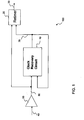
- FIG. 1 illustrates a portion of a typical receiver that includes a clock and data recovery circuit ("CDR") 100.
- the clock and data recovery circuit 100 utilizes a clock recovery circuit 10 and a retimer 20 to generate recovered data 30.
- incoming data 40 is amplified by one or more buffer stages 50 and the clock recovery circuit 10 generates an extracted clock signal 70 that has a phase and/or frequency that is fixed relative to the phase and/or frequency of the incoming amplified data 80.
- the clock recovery circuit 10 may comprise a phase lock loop or delay lock loop that aligns the edges of the extracted clock, for example the rising edge, with the transition edges of the incoming data.
- the falling edge of the clock is approximately in the middle of the incoming data symbol.
- the retimer 20 may comprise, by way of example, a falling edge flip-flop that is triggered to recover the transmitted data on the falling edge of the clock.
- typical high speed receivers may include an adaptive equalizer, such as, for example, a decision feedback equalizer (“DFE”) that may cancel inter-symbol interference.
- DFE decision feedback equalizer
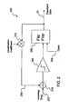
- FIG. 2 is a simplified block diagram of a conventional one tap decision feedback equalizer 200 where a summer 210 combines incoming data 220 with a feedback signal 230.
- a slicer 240 converts the output of the summer (soft decision) to a binary signal.
- a flip-flop 250 recovers the data from the binary signal in response to a clock 260.
- a multiplier 270 multiples the recovered data by an equalization coefficient (typically a negative number) to generate a scaled feedback signal 230 (typically a negative number) that is then combined with incoming data.
- the equalizer therefore serves to subtract a previous symbol from a current symbol to reduce or eliminate channel induced distortion such as inter-symbol interference.
- FIG. 3 is a simplified block diagram of a decision feedback equalizer and clock and data recovery circuit based receiver 300.
- incoming data is again amplified by one or more buffer stages 310.
- a clock recovery circuit 320 generates an extracted clock 330 from the amplified data (D1) and drives the decision feedback equalizer flip-flop 340 that recovers the equalized (D2) data provided by slicer 350.
- the clock recovery circuit 320 may align the rising edge of the extracted clock 330 with the transition edge of the amplified data D1.
- the rising edge of the extracted clock 330 should be aligned with the equalized data (D2) output by the slicer 350 for effective data recovery by flip-flop 340. Therefore, the time delay through summer 360 and slicer 350 should be equal to the time delay through buffer stage(s) 310 to ensure that the input data (D2) and clock signal 330 of flip-flop 340 are aligned to properly recover the equalizer data.
- conventional receivers typically include delay matching stages (not shown) to adjust the delay through the buffer stage(s) 310 to match the delay through summer 360 and slicer 350 to align the binary signal (D2) and extracted clock signal 330.
- the high speed receiver components may require relatively large amounts of current and dissipate relatively large amounts of heat.
- the high speed components may be implemented using shunt peaking techniques and on-chip spiral inductors. As a result, these components may occupy a relatively large area on the silicon chip.
- the use of these components may result in a design with longer interconnect lines and corresponding larger parasitic capacitance. These characteristics may have a negative impact on the performance of the system.
- the invention relates to integrated receiver components such as an integrated decision feedback equalizer and clock and data recovery circuit or components thereof.
- one or more flip-flops and/or latches are shared by a decision feedback equalizer and a clock recovery circuit to provide an integrated decision feedback equalizer and clock and data recovery circuit.
- one or more flip-flops and/or latches are used in retiming operations in a decision feedback equalizer and in phase detection operations in a clock recovery circuit.
- the output of a slicer in a decision feedback equalizer drives a pair of flip-flops connected in series.
- the flip-flops comprise a pair of latches.
- the outputs of the two flip-flops are used to generate feedback signals for the decision feedback equalizer.
- the output of the first flip-flop and the output of each of the latches in the second flip-flop are used to generate signals that drive a charge pump in the clock recovery circuit. In this circuit, the output of the second flip-flop provides the recovered data.
- the above embodiment may provide a circuit with fewer high-speed flip-flops as compared to some conventional receivers. As a result, the resulting circuit may advantageously be made smaller and may dissipate less power.
- one or more flip-flops are used in retiming operations in a decision feedback equalizer and in triwave phase detection operations in a clock recovery circuit.
- the output of a slicer in a decision feedback equalizer drives three flip-flops connected in series.
- the flip-flops comprise a pair of latches.
- the outputs of the flip-flops are used to generate feedback signals for the decision feedback equalizer.
- the output of the first flip-flop, the output of each of the latches in the second flip-flop and the output of the first latch in the third flip-flop are used to generate signals that drive a charge pump in the clock recovery circuit.
- the output of the third flip-flop provides the recovered data.
- integration techniques as taught herein may be applied to decision feedback equalizers with different numbers of feedback paths.
- integrated latches may be employed in decision feedback equalizers with one, two or more feedback paths.
- an integrated decision feedback equalizer and clock and data recovery circuit comprising:
- the decision feedback equalizer generates a binary data signal; the clock recovery circuit generates an extracted clock signal; the flip-flop is coupled to receive the binary data signal and the extracted clock signal to generate a flip-flop output signal; and the flip-flop output signal is provided to the decision feedback equalizer to provide a first feedback signal and is provided to the clock recovery circuit to provide a first phase detector signal.
- the circuit comprises a plurality of latches coupled to receive the flip-flop output signal to generate latch output signals, wherein the latch output signals comprise at least one second feedback signal for the decision feedback equalizer and second phase detector signals for the clock recovery circuit.
- the circuit comprises an XOR circuit coupled to receive the binary data signal, the first phase detector signal and the second phase detector signals to generate at least one phase detector output signal.
- the circuit comprises a charge pump coupled to receive the at least one phase detector output signal.
- the circuit comprises:
- the equalizer comprises:
- the equalizer comprises:
- the flip-flop output signal comprises a recovered data signal.
- one of the latch output signals comprises a recovered data signal.
- an integrated decision feedback equalizer and clock and data recovery circuit comprising:
- the circuit comprises a plurality of XOR circuits coupled to receive the binary data signal, the first output signal and at least a portion of the second output signals to generate the at least one phase detector output signal.
- the circuit comprises at least one multiplier coupled to receive at least a portion of the second output signals to generate the at least one scaled feedback signal.
- the extracted clock signal clocks the flip-flop and the latches; and at least two of the latches are clocked by different polarities of the extracted clock signal.
- an integrated decision feedback equalizer and clock and data recovery circuit comprises:
- the third output signal comprises a recovered data signal.
- the circuit comprises:
- the fifth output signal comprises a recovered data signal.
- a method of recovering data from a received data signal comprising:
- the first output signal comprises a recovered data signal.
- the method comprises generating at least one input signal for a charge pump by XORing pairs of signals selected from the group consisting of the binary data signal, the first output signal, the second output signal and the third output signal.
- the first latch and the second latch are clocked by different polarities of the extracted clock signal.
- the method comprises generating the at least one scaled feedback signal by multiplying the third output signal by a second equalization coefficient.
- the third output signal comprises a recovered data signal.
- the method comprises:
- the fifth output signal comprises a recovered data signal.
- the method comprises generating at least one phase detector output signal by performing XOR operations on the binary data signal, the first output signal, the second output signal, the third output signal and the fourth output signal.
- the third latch and the fourth latch are clocked by different polarities of the extracted clock signal.
- an integrated retimer and phase detector comprises:
- the second output signal comprises a second feedback signal for the decision feedback equalizer.
- the first latch and the second latch are clocked by different polarities of the extracted clock signal.
- the detector comprises an XOR circuit coupled to receive the binary data signal, the first phase detector signal, the second phase detector signal and the third phase detector signal to generate at least one phase detector output signal.
- the detector comprises:
- the third latch and the fourth latch are clocked by different polarities of the extracted clock signal.
- the detector comprises an XOR circuit coupled to receive the binary data signal, the first phase detector signal, the second phase detector signal, the third phase detector signal and the fourth phase detector signal to generate at least one phase detector output signal.
- a method of retiming data and generating phase detector signals comprising:
- the method comprises:
- the first latch and the second latch are clocked by different polarities of the extracted clock signal.
- an XOR circuit is coupled to receive the binary data signal, the first output signal, the second output signal and the third output signal to generate the at least one phase detector output signal.
- the method comprises:
- the third latch and the fourth latch are clocked by different polarities of the extracted clock signal.
- an XOR circuit is coupled to receive the binary data signal, the first output signal, the second output signal, the third output signal and the fourth output signal to generate the at least one phase detector output signal.
- FIG. 4 illustrates one embodiment of a two tap decision feedback equalizer 410 combined with a clock recovery circuit 420 for a high performance receiver 400.
- summer 430 combines an incoming data signal 440 with two equalized feedback signals 450A and 450B.
- a slicer 460 converts the output of the summer (a soft decision data signal) to a binary data signal (D).
- a binary data signal (D) output by the slicer 460 directly drives the data input of flip-flop 470 as well as the clock recovery circuit 420.
- the clock recovery circuit 420 therefore generates an extracted clock signal 412 from the binary signal (D) output by the slicer rather than from the incoming data 440 as may be done in conventional receivers (see FIG. 3).
- the clock recovery circuit 420 may align the rising edge of the extracted clock, for example, with transitions in the binary signal (D) output by the slicer 460. Therefore, the illustrated embodiment may maintain the proper timing relationship between the drive data (D) and the clock (e.g., the extracted clock signal 412) for the flip-flop 470 to ensure effective data recovery.
- the clock recovery circuit 420 includes a phase detector 414, a charge pump 416, a loop filter 418 and a voltage controlled oscillator (“VCO") 422.
- the extracted clock 412 generated by the VCO is fed back to the phase detector 414.
- the phase detector 414 compares the transition edge of the data signal (D) with an edge of the extracted clock and generates a corresponding phase error signal that is sent to the charge pump 416.
- the charge pump 416 produces a current that corresponds to the phase error signal and provides this current to the loop filter 418.
- the loop filter 418 removes selected undesirable frequency components from the current signal and sends a corresponding voltage signal to the VCO 422.
- the VCO 422 then adjusts the extracted clock phase according to this voltage signal.
- the extracted clock signal 412 output by the clock recovery circuit 420 also is used to clock the decision feedback equalizer flip-flops 470 and 472 that recover the data from the binary signal (D). Specifically, the extracted clock signal 412 is used to clock the binary signal (D) into flip-flop 470. In addition, the extracted clock signal 412 clocks the output of flip-flop 470 into flip-flop 472. In this two tap decision feedback equalizer implementation, the output of the second flip-flop 472 generates a recovered data signal 424 that provides equalized data that has been recovered from the incoming data signal 440.
- a multiplier 480A scales the recovered equalized data output by flip-flop 470 by an equalization coefficient (g1) to generate a scaled equalized feedback signal 450A.
- a multiplier 480B scales the recovered equalized data output from the flip-flop 472 by an equalization coefficient (g2) to generate another scaled equalized feedback signal 450B.
- the value of the equalization coefficients depends on the level of inter-symbol interference that is present in the incoming data. Typically the absolute value of an equalization coefficient (usually a negative number) increases with increasing inter-symbol interference.
- a real time optimization loop (not shown), such as a least mean square optimization loop, monitors the bit error rate of the equalized signal and adjusts the value of the equalization coefficient in response to changes in the bit error rate.
- Summer 430 combines the equalized feedback signals 450A and B (typically negative numbers) with the incoming data 440.
- the summer therefore subtracts a scaled version of the previous symbols from a current (that is, current, in time) symbol to reduce or eliminate channel induced distortion such as inter-symbol interference. Therefore, in this embodiment, equalized data (i.e. data that has been processed to remove inter-symbol interference) drives the clock recovery circuit 420.
- equalized data i.e. data that has been processed to remove inter-symbol interference
- the clock recovery circuit 420 may more readily lock onto the binary signal (D) as compared to circuits that lock onto the incoming data 440.
- phase detector may be implemented in various ways. Typically, a phase detector consist of one or more flip-flop(s) and logic gate(s).
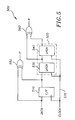
- FIG. 5 illustrates one embodiment of an extended linear phase detector 500 that includes two flip-flops 510 and 520 and an XOR circuit that includes two XOR gates 550 and 560. Since a flip-flop may consist of two latches, the second flip-flop 520 is depicted as two latches 530 and 540.
- the two flip-flops 510 and 520 clock data on the falling edge of the clock 570.
- the two latches 530 and 540 are clocked by different polarities of the clock signal 570.
- latch 530 samples (i.e., passes) its input signal when the clock signal 570 is high and holds its output signal when the clock signal 570 is low.
- the latch 540 samples when the clock signal 570 is low and holds when the clock signal 570 is high.
- the XOR circuit generates a pair of phase detector output signals.
- the data input and data output signals for the first flip-flop 510 provide internal phase detector signals for the first XOR 550.
- the XOR 550 generates a phase detector output signal P that has a pulse width proportional to data/clock phase error.
- the data output signal of the first latch 530 and the data output signal of the second latch 540 provide internal phase detector signals for the second XOR 560.
- the XOR 560 generates a phase detector output signal R that is used as a reference for phase error evaluation.
- phase detector flip-flops may be relatively challenging because they operate at a high rate of speed. For example, data delays between and within the flip-flops and latches must be accounted for to ensure that the correct data is being latched.
- the flip-flop and latch implementation in FIG. 5 may advantageously be used to provide a CMOS phase detector that operates properly at frequencies on the order of 10 GHz.
- phase detector similar to the one depicted in FIG. 5 is described in U.S. Patent Application No. 10/293,163 filed November 12, 2002, the disclosure of which is incorporated herein by reference. See, for example, FIG. 4 and the accompanying disclosure.
- FIG. 6 illustrates one embodiment of an integrated two tap decision feedback equalizer and clock and data recovery circuit 600.
- a phase detector 630 in a clock and data recovery circuit 620 incorporates the design of the phase detector 500 of FIG. 5.
- the architecture of the receiver includes an integrated phase detector and retimer to reduce the number of high-speed components in the receiver. That is, the CDR phase detector flip-flops (flip-flop 610 and latch pair 612 and 614) also function as DFE retimers. These flip-flops may be shared because in the architecture of FIG. 6 the flip-flops for a CDR phase detector may operate from the same signals (e.g., binary data signal (D) and an extracted clock signal 640) as the flip-flops for a DFE retimer.
- D binary data signal
- an extracted clock signal 640 extracted clock signal
- the data outputs signals from the two flip-flops also provide the DFE tap signals for the DFE feedback loop.
- the output signals 660A and 660B are multiplied by equalization coefficients g1 and g2 at multipliers 680A and 680B, respectively, then provided to a summer 650.
- a slicer 652 digitizes the output of the summer 650 to generate the binary data signal (D) that is provided to the first flip-flop 610.
- the output of the second flip-flop provides the recovered data signal 670.
- the P and R outputs of the phase detector 630 are fed to a charge pump 690.
- the charge pump 690 provides a current to a loop filter 692 which provides a voltage signal to VCO 694.
- the VCO 694 generates the extracted clock signal 640 that clocks the two flip-flops.
- the DFE high-speed blocks are the summer, limiter and the flip-flops.
- the high-speed blocks are mainly the VCO and the phase detector flip-flops.
- the extracted clock signal typically is the fastest signal on the chip (e.g., 10GHz, whereas the fastest data signal may be 10Gbps), and its relatively high load effect may limit the maximum operational speed of the chip.
- the elimination of DFE flip-flops may be significant for enabling DFE based receiver functionality at 10Gbps in CMOS technology.
- a flip-flop is almost twice as large as a buffer (e.g., a summer, limiter, etc) and may consume twice as much power.
- reducing the number of flip-flops may advantageously impact the implementation of other components in the receiver.
- the VCO drives only 2 flip-flops in the embodiment of FIG. 6, instead of 4 flip-flops as in FIG. 4, the capacitive loading on the VCO is reduced significantly.
- the slicer drives only the phase detector, the slicer sees a smaller capacitive load (as compared to circuits where the slicer drives DFE flip-flop(s) as well) and hence requires less current.
- these components may be made smaller and other design problems associated with a high speed, high current implementation of such components (e.g., noise and shielding) may be reduced or avoided.
- the elimination of two high speed flip-flops as provided by the embodiment of FIG. 6 may provide a circuit with smaller silicon die area, shorter interconnect lines (with a corresponding reduction in parasitic components), significantly lower power consumption and other advantages.
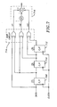
- FIG. 7 depicts a simplified block diagram of one embodiment of a triwave phase detector.
- the triwave phase detector includes flip-flops 708, 710 and 712, an XOR circuit 714 and an optional summer circuit 716.
- data jitter dependence of the CDR is reduced in comparison to a traditional Hogge detector.
- the triwave phase detector generates three outputs U1, U2 and U3 that may be sent to a charge pump.
- the output stage of the triwave phase detector may include a circuit (e.g., circuit 716) that provides the summation of U1 and U3 minus 2U2.
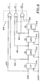
- FIG. 8 depicts one embodiment of a modified triwave phase detector that accommodates the sharing of flip-flops with the DFE in accordance with the invention.
- the second flip-flop (falling edge triggered flip-flop 710) in FIG. 7 is replaced in FIG. 8 with a rising edge triggered flip-flop (represented by latches 812 and 816). This transformation of falling edge to rising edge flip-flop enables sharing of DFE flip-flops.
- the third flip-flop 712 in FIG. 7 is replaced in FIG. 8 with a single latch 816 (the second latch for this flip-flop may be eliminated for the phase detector).
- the flip-flop and the latches provide phase detector input signals for an XOR circuit 828 that generates phase detector output signals U1, U2 and U3.
- the U1 phase detector signal is generated from signals 818 and 820 in a manner similar to that depicted in FIG. 7. However, in contrast with FIG. 7, the output signal 822 of latch 812 and the output signal 824 of latch 814 are used to generate U2 in the phase detector of FIG. 8. In addition, the output signal 824 of latch 814 and the output signal 826 of latch 816 are used to generate U3 in FIG. 8 in contrast with the circuit of FIG. 7.
- the modified triwave phase detector of FIG. 8 may be used to provide signals U1, U2, and U3 that have waveforms that are be identical to the waveforms for the triwave phase detector of FIG. 7.
- FIG. 9 depicts one embodiment of a 3 tap DFE that shares 3 flip-flops (flip-flop 912, latch pair 914 and 916, and latch pair 918 and 920) of a phase detector 910.
- a total of three high-speed flip-flops may be eliminated as compared to some conventional approaches.
- the U1, U2 and U3 output signals of the phase detector 910 are provided to a charge pump 928 in the CDR 930.
- the charge pump 928 generates a current to drive loop filter 922 which in turn drives VCO 924.
- the VCO 924 generates an extracted clock signal 944 that clocks the flip-flops.
- Multipliers 932A, 932B and 932C multiply the respective outputs of the three flip-flops by equalization coefficients g1, g2 and g3, respectively, to provide feedback signals to the summer 940.
- the resulting summed signal is processed by slicer 942 to generate the input data (D) for the CDR 930.
- the output 950 of the third flip-flop (the output of latch 920) provides the recovered data.
- FIG. 10 illustrates one embodiment of an integrated one tap decision feedback equalizer and clock and data recovery circuit 1000.
- the output of the first phase detector flip-flop 1010 is multiplied by g1 at multiplier 1012 and only this signal is fed back to the summer 1014.
- the output of the first flip-flop 1010 also provides the recovered data 1020.
- the extracted clock signal 1048 that clocks the two flip-flops is generated by the phase detector 1030, charge pump 1042, loop filter 1044 and VCO 1046 in the CDR 1040 as described above.
- the integration of the DFE and the CDR provides an effective elimination of one flip-flop.
- This topology may be used with many different phase detectors because it only requires one flip-flop for the DFE.
- the CDR may incorporate a Hogge phase detector or a binary phase detector.
- the phase detector of FIG. 10 may provide the first two taps.
- the remaining taps may be provided by flip-flops in the DFE.
- FIG. 11 illustrates one embodiment of an integrated three tap decision feedback equalizer and clock and data recovery circuit 1100.
- the CDR 1114 operates essentially as discussed above in conjunction with FIG. 10. With the addition of a DFE flip-flop 1112, however, the output of the second flip-flop (the output of latch 1124) provides the data input for the DFE flip-flop 1112 and the extracted clock signal 1126 also clocks the DFE flip-flop 1112. In addition, the output signals from the three flip-flops (flip-flop 1120, latch pair 1122 and 1124 and flip-flop 1112) are fed back to the summer 1110. The output of the DFE flip-flop 1112 provides the recovered data 1116.
- a receiver with a four tap DFE may incorporate two flip-flops in the phase detector and two additional flip-flops as part of the DFE. In this case, a total of 4 flip-flops would be necessary as opposed to six flip-flops that may be required if this topology was not used. It should thus be understood that the teachings discussed herein may be incorporated into other multi-tap DFEs.
- phase detector structures that do not readily lend themselves to flip-flop and/or latch sharing may, in many cases, be modified to enable such sharing. Moreover, this may be accomplished without compromising the performance of the phase detector. Such a modification is discussed above, for example, in conjunction with the embodiment of FIG. 9.
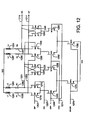
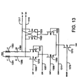
- FIGS. 12 and 13 describe example embodiments of a shunt peaking flip-flop and a shunt peaking latch, respectively, that may be used in a high speed CMOS receiver constructed according to the teachings herein.
- the flip-flops and latches have differential clock and data inputs and differential data outputs.
- FIGS. 12 and 13 illustrate that the flip-flop may be constructed of two latches connected in series as discussed above.
- FIG. 12 is a schematic of one embodiment of a negative-edge triggered flip-flop based on current controlled CMOS (C 3 MOS) logic with shunt peaking (e.g., inductive broadbanding) aspects. Additional details of C 3 MOS logic with inductive broadbanding is described in commonly owned U.S. Patent Application No. 09/610,905, filed July 6, 2000, the disclosure of which is incorporated herein by reference.
- C 3 MOS current controlled CMOS
- the flip-flop of FIG. 12 comprises two latches, a master and a slave, in series.
- the master latch includes input differential pair M1 1210 and M2 1215, latching devices M3 1220 and M4 1225, clock pair M9 1250 and M10 1255, current source M14 1270, and series combination loads L1 1281 and R1 1285, and L2 1283 and R2 1290.
- the slave latch includes input differential pair M5 1230 and M6 1235, latching devices M7 1240 and M8 1245, clock pair M11 1260 and M12 1265, current source M15 1280, and series combination loads L3 1287 and R3 1295, and L4 1291 and R4 1297.
- Data input signals DIP and DIN are received on lines 1202 and 1207
- clock input signals CKP and CKN are received on lines 1209 and 1211
- a bias voltage signal BIASN is received on line 1279
- output signals QP (true) and QN (complementary) are provided on lines 1217 and 1219.
- the power supply signals as shown here as VDD and VSS. Additional details of the operation and construction of these components is provided in U.S. Patent Application No. 10/293,163, filed November 12, 2002.
- FIG. 13 is a schematic of one embodiment of a latch incorporating inductive broadbanding.
- the latch includes input differential pair M1 1310 and M2 1315, latching devices M3 1320 and M4 1325, clock pair M5 1350 and M6 1355, current source M7 1370, and series combination loads L1 1381 and R1 1385, and L2 1383 and R2 1390.
- Data input signals DIP and DIN are received on lines 1302 and 1307
- clock input signals CKP and CKN are received on lines 1309 and 1311
- a bias voltage signal BIASN is received on line 1379
- output signals QP (true) and QN (complementary) are provided on lines 1317 and 1319.
- the power supply signals as shown here as VDD and VSS.
- flip-flops and latches may be used including for example, bi-polar devices, devices made of GaAs on silicon, or other types of devices.
- Another embodiment of a flip-flop is described in commonly owned U.S. Patent Application Number 09/784,419, filed February 15, 2002, the disclosure of which is incorporated herein by reference.
- current source loads p-channel loads operating in their triode regions, or source follower outputs may be used.
- N-channel metal oxide semiconductor field effect transistors MOSFET, or NMOS
- PMOS p-channel
- the integrated decision feedback equalizer and clock and data recovery circuits described herein may be integrated into any of a variety of applications.
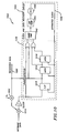
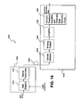
- the described exemplary integrated decision feedback equalizer and clock and data recovery circuit may be incorporated into the optical receiver assembly 1410 of an optical communication system 1400.
- the optical system 1400 includes an optical transmitter 1420 and an optical fiber network 1430 that carries the optical signal to the optical receiver assembly 1410.
- optical transmitter 1420 and an optical fiber network 1430 that carries the optical signal to the optical receiver assembly 1410.
- the illustrated receive path includes an optical detector 1435, sensing resistor 1440, one or more amplifier(s) 1450, and an integrated decision feedback equalizer and clock and data recovery circuit 1460.
- the optical detector 1435 may comprise a known prior art optical detector implementation. Such prior art detectors convert incoming optical signals into corresponding electrical output signals that may be electronically monitored.
- a transmit path includes, by way of example, one or more gain stage(s) 1470 coupled to an optical transmitter 1475.
- the gain stage(s) 1470 may have multiple stages, and may receive one or more control signals for controlling various different parameters of the output of the optical transmitter.
- an analog data source provides an analog data signal that modulates the output of the optical transmitter.
- baseband digital modulation or frequency modulation may be used.
- the gain stage(s) 1470 amplify the incoming data signal from the data source according to laser control signals.
- the amplified data signal drives the optical transmitter 1475.
- the optical transmitter may, for example, be a light emitting diode or a surface emitting laser or an edge emitting laser that operate at high speeds such as 10 Gigabits per second (Gbps) or higher.
- the optical transmitter 1475 thereby generates an optical data signal that provided to a fiber optic cable 1430.
- the fiber optic cable 1430 carries the optical data signal to the optical detector 1435.
- the transmit optical beam is incident on a light receiving surface area of the optical detector, electron-hole pairs are generated.
- a bias voltage applied across the optical detector 1435 generates a flow of electric current having an intensity proportional to the intensity of the incident light. In one embodiment, this current flows through sensing resistor 1440, and generates a voltage.
- the sensed voltage is amplified by the one or more amplifier(s) 1450 and the output of amplifier(s) 1450 drives the integrated decision feedback equalizer and clock and data recovery circuit 1460.
- the decision feedback equalizer may include, by way of example, a slicer that generates a binary signal (D) that drives a clock and data recovery circuit.
- the clock and data recovery circuit generates an extracted clock signal from the binary signal that is then used to retime the equalized data as discussed above.
- a receiver constructed according to the invention may support various data protocols and date rates.
- the receiver is a multi-rate SONET/SDH/10GE/FEC receiver that may operate at very high speeds including, for example, 9.953, 10.3125, 10.664 or 10.709 Gbps.
- This receiver includes, in a single chip solution, an optical equalizer and CDR as discussed above, a linear amplifier, deserializer and other components.
- the receiver chip is implemented using CMOS technology.
- CMOS technology complementary metal-oxide-semiconductor
- Different embodiments of the invention may include a variety of hardware and software processing components.
- hardware components such as controllers, state machines and/or logic are used in a system constructed in accordance with the invention.
- code such as software or firmware executing on one or more processing devices may be used to implement one or more of the described operations.
- Such components may be implemented on one or more integrated circuits. For example, in some embodiments several of these components may be combined within a single integrated circuit. In some embodiments some of the components may be implemented as a single integrated circuit. In some embodiments some components may be implemented as several integrated circuits. For example, in one embodiment the integrated DFE and CDR may be implemented on a single receiver chip.
- connections represented by the lead lines in the drawings may be in an integrated circuit, on a circuit board and/or over a backplane to other circuit boards.
- some of the connections represented by the lead lines in the drawings may comprise a data network, for example, a local network and/or a wide area network (e.g., the Internet).
- a signal may be an electrical signal transmitted over a wire while other signals may consist of light pulses transmitted over an optical fiber.
- a signal may comprise more than one signal.
- a differential signal comprises two complementary signals or some other combination of signals.
- Signals as discussed herein also may take the form of data.
- an application program may send a signal to another application program.
- Such a signal may be stored in a data memory.
- the components and functions described herein may be connected/coupled directly or indirectly. Thus, in some embodiments there may or may not be intervening devices (e.g., buffers) between connected/coupled components.
- intervening devices e.g., buffers
- the invention described herein generally relates to an improved communications receiver. While certain exemplary embodiments have been described above in detail and shown in the accompanying drawings, it is to be understood that such embodiments are merely illustrative of and not restrictive of the broad invention. In particular, it should be recognized that the teachings of the invention apply to a wide variety of systems and processes. It will thus be recognized that various modifications may be made to the illustrated and other embodiments of the invention described above, without departing from the broad inventive scope thereof. In view of the above it will be understood that the invention is not limited to the particular embodiments or arrangements disclosed, but is rather intended to cover any changes, adaptations or modifications which are within the scope and spirit of the invention as defined by the appended claims.
Landscapes
- Engineering & Computer Science (AREA)
- Computer Networks & Wireless Communication (AREA)
- Signal Processing (AREA)
- Power Engineering (AREA)
- Cable Transmission Systems, Equalization Of Radio And Reduction Of Echo (AREA)
- Synchronisation In Digital Transmission Systems (AREA)
- Dc Digital Transmission (AREA)
- Manipulation Of Pulses (AREA)
Applications Claiming Priority (4)
| Application Number | Priority Date | Filing Date | Title |
|---|---|---|---|
| US823252 | 2001-03-30 | ||
| US53109403P | 2003-12-19 | 2003-12-19 | |
| US531094P | 2003-12-19 | ||
| US10/823,252 US7822113B2 (en) | 2003-12-19 | 2004-04-13 | Integrated decision feedback equalizer and clock and data recovery |
Publications (2)
| Publication Number | Publication Date |
|---|---|
| EP1545045A2 true EP1545045A2 (de) | 2005-06-22 |
| EP1545045A3 EP1545045A3 (de) | 2006-01-04 |
Family
ID=34527151
Family Applications (1)
| Application Number | Title | Priority Date | Filing Date |
|---|---|---|---|
| EP04028869A Withdrawn EP1545045A3 (de) | 2003-12-19 | 2004-12-06 | Integrierte entscheidungsrückgekoppelte Entzerrung und Takt- und Daten-Rückgewinnung |
Country Status (4)
| Country | Link |
|---|---|
| US (1) | US7822113B2 (de) |
| EP (1) | EP1545045A3 (de) |
| CN (1) | CN1638367B (de) |
| TW (1) | TWI262686B (de) |
Cited By (5)
| Publication number | Priority date | Publication date | Assignee | Title |
|---|---|---|---|---|
| EP1814254A1 (de) * | 2006-01-26 | 2007-08-01 | Alcatel Lucent | Binärer Phasendetektor und Schaltung zur Takt- und Datenrückgewinnung |
| KR100801055B1 (ko) | 2006-10-16 | 2008-02-04 | 삼성전자주식회사 | 데이터 수신기 및 이를 구비하는 반도체 장치 |
| WO2008085299A1 (en) | 2007-01-09 | 2008-07-17 | Rambus Inc. | Receiver with clock recovery circuit and adaptive sample and equalizer timing |
| EP2741420A1 (de) * | 2012-12-10 | 2014-06-11 | Nxp B.V. | Lokale Oszillatorsignalerzeugung |
| US8774337B2 (en) | 2006-04-04 | 2014-07-08 | Rambus Inc. | Phase control block for managing multiple clock domains in systems with frequency offsets |
Families Citing this family (65)
| Publication number | Priority date | Publication date | Assignee | Title |
|---|---|---|---|---|
| US7627029B2 (en) | 2003-05-20 | 2009-12-01 | Rambus Inc. | Margin test methods and circuits |
| US7590175B2 (en) | 2003-05-20 | 2009-09-15 | Rambus Inc. | DFE margin test methods and circuits that decouple sample and feedback timing |
| US7443913B2 (en) * | 2004-02-12 | 2008-10-28 | Texas Instruments Incorporated | High speed decision feedback equalizer |
| US7623600B2 (en) | 2004-06-02 | 2009-11-24 | Broadcom Corporation | High speed receive equalizer architecture |
| US7697603B1 (en) * | 2004-10-18 | 2010-04-13 | Altera Corporation | Methods and apparatus for equalization in high-speed backplane data communication |
| GB2422989A (en) * | 2005-02-03 | 2006-08-09 | Agilent Technologies Inc | Correlating a received data signal with a time delayed version of the signal to obtain a measurement of inter-symbol interference |
| US7519139B1 (en) * | 2005-07-20 | 2009-04-14 | Lattice Semiconductor Corporation | Signal monitoring systems and methods |
| US7526023B1 (en) * | 2005-09-08 | 2009-04-28 | Altera Corporation | Programmable cross-talk cancellation in programmable logic device |
| US9014252B2 (en) * | 2006-09-15 | 2015-04-21 | Lsi Corporation | Band-pass high-order analog filter backed hybrid receiver equalization |
| KR100791635B1 (ko) | 2006-09-28 | 2008-01-04 | 고려대학교 산학협력단 | 고속 적응형 이퀄라이저 |
| US8184686B2 (en) * | 2007-01-10 | 2012-05-22 | Cortina Systems, Inc. | System and method for recovering data received over a communication channel |
| US7983333B2 (en) * | 2007-02-09 | 2011-07-19 | Broadcom Corporation | Non-linear analog decision feedback equalizer |
| US7615389B2 (en) * | 2007-05-31 | 2009-11-10 | Corning Incorporated | GaN lasers on ALN substrates and methods of fabrication |
| US7692501B2 (en) * | 2007-09-14 | 2010-04-06 | Intel Corporation | Phase/frequency detector and charge pump architecture for referenceless clock and data recovery (CDR) applications |
| US8270464B2 (en) * | 2008-06-20 | 2012-09-18 | Fujitsu Limited | Decision feedback equalizer (DFE) |
| US8503519B2 (en) * | 2008-06-20 | 2013-08-06 | Fujitsu Limited | Detecting residual ISI components using two data patterns |
| US20100020862A1 (en) * | 2008-07-25 | 2010-01-28 | Taiwan Semiconductor Manufacturing Co., Ltd. | Input control circuit for the summer of a decision feedback equalizer |
| KR100965767B1 (ko) | 2008-09-08 | 2010-06-24 | 주식회사 하이닉스반도체 | 클럭 복원 회로를 구비하는 결정 피드백 등화기 및 클럭 복원 방법 |
| US7872823B2 (en) * | 2009-01-12 | 2011-01-18 | Lsi Corporation | AGC loop with weighted zero forcing and LMS error sources and methods for using such |
| KR100989848B1 (ko) * | 2009-08-31 | 2010-10-29 | 동국대학교 산학협력단 | 클럭 및 데이터 복원 회로 |
| US8259784B2 (en) * | 2010-03-26 | 2012-09-04 | Realtek Semiconductor Corp. | High-speed continuous-time feedback equalizer for serial link receiver |
| CN102480446B (zh) * | 2010-11-29 | 2014-08-20 | 瑞昱半导体股份有限公司 | 接收机均衡器校正装置与方法 |
| TWI445335B (zh) * | 2011-03-16 | 2014-07-11 | Realtek Semiconductor Corp | 等化器與等化方法 |
| US8817862B2 (en) * | 2011-03-16 | 2014-08-26 | Realtek Semiconductor Corp. | Equalizer and equalizing method |
| US8509299B2 (en) | 2011-07-21 | 2013-08-13 | National Semiconductor Corporation | Decision feedback equalizer operable with multiple data rates |
| CN102299721A (zh) * | 2011-09-22 | 2011-12-28 | 四川和芯微电子股份有限公司 | 均衡电路及均衡系统 |
| WO2013063586A1 (en) * | 2011-10-28 | 2013-05-02 | Ofs Fitel, Llc | Distributed feedback (dfb) brillouin fiber lasers |
| US8976855B2 (en) * | 2013-03-14 | 2015-03-10 | Intel Corporation | Power and area efficient receiver equalization architecture with relaxed DFE timing constraint |
| US8958513B1 (en) * | 2013-03-15 | 2015-02-17 | Xilinx, Inc. | Clock and data recovery with infinite pull-in range |
| KR102241045B1 (ko) | 2013-04-16 | 2021-04-19 | 칸도우 랩스 에스에이 | 고 대역폭 통신 인터페이스를 위한 방법 및 시스템 |
| CN103491038B (zh) * | 2013-10-16 | 2016-05-18 | 清华大学 | 用于高速串行接口接收端的1/4速率4抽头判决反馈均衡器 |
| CN104280613B (zh) * | 2014-10-15 | 2017-03-08 | 成都振芯科技股份有限公司 | 一种片内信号间的相位检测与同步电路及其同步方法 |
| US9755653B2 (en) | 2014-11-05 | 2017-09-05 | Mediatek Inc. | Phase detector |
| JP6554956B2 (ja) * | 2015-07-14 | 2019-08-07 | 富士通株式会社 | 位相検出回路および信号再生回路 |
| CN109314518B (zh) | 2016-04-22 | 2022-07-29 | 康杜实验室公司 | 高性能锁相环 |
| US10193716B2 (en) | 2016-04-28 | 2019-01-29 | Kandou Labs, S.A. | Clock data recovery with decision feedback equalization |
| US10411922B2 (en) | 2016-09-16 | 2019-09-10 | Kandou Labs, S.A. | Data-driven phase detector element for phase locked loops |
| US10075308B2 (en) * | 2016-09-30 | 2018-09-11 | Intel Corporation | Supply voltage adaptation via decision feedback equalizer |
| US10372665B2 (en) | 2016-10-24 | 2019-08-06 | Kandou Labs, S.A. | Multiphase data receiver with distributed DFE |
| CN110945830B (zh) | 2017-05-22 | 2022-09-09 | 康杜实验室公司 | 多模式数据驱动型时钟恢复电路 |
| US10911269B2 (en) * | 2017-07-06 | 2021-02-02 | Intel Corporation | Decision feedback equalizer circuit with transistor mobility change compensation |
| US10091031B1 (en) * | 2017-07-31 | 2018-10-02 | Micron Technology, Inc. | Apparatus having a data receiver with a real time clock decoding decision feedback equalizer |
| US10326623B1 (en) | 2017-12-08 | 2019-06-18 | Kandou Labs, S.A. | Methods and systems for providing multi-stage distributed decision feedback equalization |
| US10373659B2 (en) * | 2017-12-21 | 2019-08-06 | Micron Technology, Inc. | Voltage reference computations for memory decision feedback equalizers |
| US10554380B2 (en) | 2018-01-26 | 2020-02-04 | Kandou Labs, S.A. | Dynamically weighted exclusive or gate having weighted output segments for phase detection and phase interpolation |
| US10931249B2 (en) | 2018-06-12 | 2021-02-23 | Kandou Labs, S.A. | Amplifier with adjustable high-frequency gain using varactor diodes |
| EP3807996B1 (de) | 2018-06-12 | 2022-07-06 | Kandou Labs SA | Kombiniertes taktdatenrückgewinnungslogiknetzwerk und ladungspumpenschaltung mit niedriger latenzzeit |
| US10637640B2 (en) * | 2018-07-22 | 2020-04-28 | SiliconIntervention Inc. | Asynchronous data recovery |
| US10566959B1 (en) * | 2018-10-24 | 2020-02-18 | Samsung Electronics Co., Ltd. | Sense amplifier flip-flop and method for fixing setup time violations in an integrated circuit |
| US10958251B2 (en) | 2019-04-08 | 2021-03-23 | Kandou Labs, S.A. | Multiple adjacent slicewise layout of voltage-controlled oscillator |
| US10608849B1 (en) | 2019-04-08 | 2020-03-31 | Kandou Labs, S.A. | Variable gain amplifier and sampler offset calibration without clock recovery |
| US10680634B1 (en) | 2019-04-08 | 2020-06-09 | Kandou Labs, S.A. | Dynamic integration time adjustment of a clocked data sampler using a static analog calibration circuit |
| KR102674031B1 (ko) | 2019-05-13 | 2024-06-12 | 삼성전자주식회사 | 메모리 컨트롤러, 이를 포함하는 메모리 시스템 및 그 동작 방법 |
| CN112187256B (zh) * | 2019-07-04 | 2023-08-25 | 智原微电子(苏州)有限公司 | 时钟数据恢复装置及其操作方法 |
| US20210049952A1 (en) * | 2019-08-13 | 2021-02-18 | Novatek Microelectronics Corp. | Light-emitting diode driving apparatus |
| US11341904B2 (en) * | 2019-08-13 | 2022-05-24 | Novatek Microelectronics Corp. | Light-emitting diode driving apparatus and light-emitting diode driver |
| CN112688701B (zh) * | 2020-12-22 | 2022-05-31 | 北京奕斯伟计算技术有限公司 | 接收机电路以及接收机电路控制方法 |
| US11463092B1 (en) | 2021-04-01 | 2022-10-04 | Kanou Labs Sa | Clock and data recovery lock detection circuit for verifying lock condition in presence of imbalanced early to late vote ratios |
| US11303484B1 (en) | 2021-04-02 | 2022-04-12 | Kandou Labs SA | Continuous time linear equalization and bandwidth adaptation using asynchronous sampling |
| US11563605B2 (en) | 2021-04-07 | 2023-01-24 | Kandou Labs SA | Horizontal centering of sampling point using multiple vertical voltage measurements |
| US11374800B1 (en) | 2021-04-14 | 2022-06-28 | Kandou Labs SA | Continuous time linear equalization and bandwidth adaptation using peak detector |
| US11456708B1 (en) | 2021-04-30 | 2022-09-27 | Kandou Labs SA | Reference generation circuit for maintaining temperature-tracked linearity in amplifier with adjustable high-frequency gain |
| CN113300703B (zh) * | 2021-05-24 | 2023-03-14 | 成都振芯科技股份有限公司 | 一种基于相位检测的自适应均衡装置及方法 |
| US11496282B1 (en) | 2021-06-04 | 2022-11-08 | Kandou Labs, S.A. | Horizontal centering of sampling point using vertical vernier |
| US12355409B2 (en) | 2022-03-24 | 2025-07-08 | Kandou Labs SA | Variable gain amplifier with cross-coupled common mode reduction |
Family Cites Families (45)
| Publication number | Priority date | Publication date | Assignee | Title |
|---|---|---|---|---|
| JPH0624315B2 (ja) * | 1983-11-04 | 1994-03-30 | 日本ビクター株式会社 | 移相器 |
| US4787097A (en) * | 1987-02-11 | 1988-11-22 | International Business Machines Corporation | NRZ phase-locked loop circuit with associated monitor and recovery circuitry |
| US4862484A (en) * | 1988-01-21 | 1989-08-29 | Harris Corporation | Apparatus for clock recovery from digital data |
| US5179302A (en) * | 1991-04-03 | 1993-01-12 | Loral Aerospace Corp. | Tunable data filter |
| US5671252A (en) * | 1994-09-21 | 1997-09-23 | Analog Devices, Inc. | Sampled data read channel utilizing charge-coupled devices |
| US5581585A (en) * | 1994-10-21 | 1996-12-03 | Level One Communications, Inc. | Phase-locked loop timing recovery circuit |
| US5684434A (en) * | 1995-10-30 | 1997-11-04 | Cypress Semiconductor | Erasable and programmable single chip clock generator |
| US5774505A (en) * | 1996-04-04 | 1998-06-30 | Hewlett-Packard Company | Intersymbol interference cancellation with reduced complexity |
| US6437932B1 (en) | 1996-05-16 | 2002-08-20 | Lsi Logic Corporation | Decision based time-varying equalizers |
| US5786951A (en) * | 1996-06-05 | 1998-07-28 | Cirrus Logic, Inc. | Sampled amplitude read channel employing a discrete time noise generator for calibration |
| US5940441A (en) * | 1996-10-29 | 1999-08-17 | International Business Machines Corporation | Integrated adaptive cable equalizer using a continuous-time filter |
| US6069522A (en) * | 1997-02-03 | 2000-05-30 | Texas Instruments Incorporated | Circuitry and method for providing boost and asymmetry in a continuous-time filter |
| US6285709B1 (en) * | 1997-10-31 | 2001-09-04 | 3 Com Corporation | Error filtering in a hybrid equalizer system |
| US6144697A (en) * | 1998-02-02 | 2000-11-07 | Purdue Research Foundation | Equalization techniques to reduce intersymbol interference |
| US6233107B1 (en) * | 1998-03-20 | 2001-05-15 | Seagate Technology Llc | Analog self-synchronization subsystem based on peak detection and post processing in a sampled channel of digital magnetic recording |
| US6064272A (en) * | 1998-07-01 | 2000-05-16 | Conexant Systems, Inc. | Phase interpolated fractional-N frequency synthesizer with on-chip tuning |
| JP3946882B2 (ja) * | 1998-09-18 | 2007-07-18 | 富士通株式会社 | 信号処理回路及び信号処理回路の制御方法 |
| GB9916907D0 (en) * | 1999-07-19 | 1999-09-22 | Cambridge Silicon Radio Ltd | Variable oscillator |
| US6968167B1 (en) * | 1999-10-21 | 2005-11-22 | Broadcom Corporation | Adaptive radio transceiver with calibration |
| US6909852B2 (en) * | 2000-02-17 | 2005-06-21 | Broadcom Corporation | Linear full-rate phase detector and clock and data recovery circuit |
| US6340899B1 (en) * | 2000-02-24 | 2002-01-22 | Broadcom Corporation | Current-controlled CMOS circuits with inductive broadbanding |
| JP2001256728A (ja) * | 2000-03-10 | 2001-09-21 | Fujitsu Ltd | 半導体装置 |
| SE517967C2 (sv) * | 2000-03-23 | 2002-08-06 | Ericsson Telefon Ab L M | System och förfarande för klocksignalgenerering |
| US6807225B1 (en) * | 2000-05-31 | 2004-10-19 | Conexant Systems, Inc. | Circuit and method for self trimming frequency acquisition |
| JP4454798B2 (ja) * | 2000-06-09 | 2010-04-21 | Necエレクトロニクス株式会社 | クロック再生装置 |
| AU2001284762A1 (en) | 2000-08-09 | 2002-02-18 | Jds Uniphase Corporation | High order fiber raman amplifiers |
| JP3532861B2 (ja) * | 2001-02-06 | 2004-05-31 | 松下電器産業株式会社 | Pll回路 |
| KR100400043B1 (ko) * | 2001-06-11 | 2003-09-29 | 삼성전자주식회사 | 데이터 복원 회로 및 방법 |
| US7092474B2 (en) * | 2001-09-18 | 2006-08-15 | Broadcom Corporation | Linear phase detector for high-speed clock and data recovery |
| US7054606B1 (en) * | 2001-09-21 | 2006-05-30 | Lsi Logic Corporation | Digitally calibrated narrowband filter with analog channel compensation |
| EP1331779B1 (de) | 2002-01-28 | 2007-04-04 | Lucent Technologies Inc. | Einstellung von Entscheidungspegeln und Abtastphase auf der Basis von vorherigen Bit-Werten |
| US20030165208A1 (en) * | 2002-03-04 | 2003-09-04 | Andrew Carter | Non-linear decision feedback phase locked loop filter |
| US7486894B2 (en) | 2002-06-25 | 2009-02-03 | Finisar Corporation | Transceiver module and integrated circuit with dual eye openers |
| US7353245B2 (en) * | 2002-09-04 | 2008-04-01 | Agere Systems Inc. | Adaptive filter coefficient determination |
| US7085328B2 (en) * | 2002-12-24 | 2006-08-01 | Realtek Semiconductor Corp. | QAM receiver having joint gain, carrier recovery and equalization adaptation system |
| US7830956B2 (en) * | 2003-02-05 | 2010-11-09 | Fujitsu Limited | Method and system for processing a sampled signal |
| US7016406B1 (en) * | 2003-04-29 | 2006-03-21 | Scintera Networks | Adaptation structure and methods for analog continuous time equalizers |
| US7190742B2 (en) * | 2003-06-19 | 2007-03-13 | Applied Micro Circuits Corporation | Differential receiver circuit with electronic dispersion compensation |
| US7471904B2 (en) * | 2003-07-25 | 2008-12-30 | Alcatel-Lucent Usa Inc. | Method and apparatus for electronic equalization in optical communication systems |
| TW589785B (en) * | 2003-08-01 | 2004-06-01 | Winbond Electronics Corp | Digitally controlled tuner circuit |
| US7302461B2 (en) * | 2003-11-26 | 2007-11-27 | Scintera Networks, Inc. | Analog delay elements |
| US7272178B2 (en) * | 2003-12-08 | 2007-09-18 | Freescale Semiconductor, Inc. | Method and apparatus for controlling the bandwidth frequency of an analog filter |
| US7330508B2 (en) * | 2003-12-19 | 2008-02-12 | Broadcom Corporation | Using clock and data recovery phase adjust to set loop delay of a decision feedback equalizer |
| US7436882B2 (en) * | 2003-12-19 | 2008-10-14 | Broadcom Corporation | Decision feedback equalizer and clock and data recovery circuit for high speed applications |
| US7522847B2 (en) * | 2003-12-19 | 2009-04-21 | Broadcom Corporation | Continuous time filter-decision feedback equalizer architecture for optical channel equalization |
-
2004
- 2004-04-13 US US10/823,252 patent/US7822113B2/en not_active Expired - Fee Related
- 2004-12-06 EP EP04028869A patent/EP1545045A3/de not_active Withdrawn
- 2004-12-17 TW TW093139279A patent/TWI262686B/zh not_active IP Right Cessation
- 2004-12-17 CN CN200410104226.2A patent/CN1638367B/zh not_active Expired - Fee Related
Non-Patent Citations (1)
| Title |
|---|
| None * |
Cited By (16)
| Publication number | Priority date | Publication date | Assignee | Title |
|---|---|---|---|---|
| EP1814254A1 (de) * | 2006-01-26 | 2007-08-01 | Alcatel Lucent | Binärer Phasendetektor und Schaltung zur Takt- und Datenrückgewinnung |
| US11063741B2 (en) | 2006-04-04 | 2021-07-13 | Rambus Inc. | Phase control block for managing multiple clock domains in systems with frequency offsets |
| US10454667B2 (en) | 2006-04-04 | 2019-10-22 | Rambus Inc. | Phase control block for managing multiple clock domains in systems with frequency offsets |
| US9912469B2 (en) | 2006-04-04 | 2018-03-06 | Rambus Inc. | Phase control block for managing multiple clock domains in systems with frequency offsets |
| US8774337B2 (en) | 2006-04-04 | 2014-07-08 | Rambus Inc. | Phase control block for managing multiple clock domains in systems with frequency offsets |
| US9106399B2 (en) | 2006-04-04 | 2015-08-11 | Rambus Inc. | Phase control block for managing multiple clock domains in systems with frequency offsets |
| US9515814B2 (en) | 2006-04-04 | 2016-12-06 | Rambus Inc. | Phase control block for managing multiple clock domains in systems with frequency offsets |
| KR100801055B1 (ko) | 2006-10-16 | 2008-02-04 | 삼성전자주식회사 | 데이터 수신기 및 이를 구비하는 반도체 장치 |
| US8548110B2 (en) | 2007-01-09 | 2013-10-01 | Rambus Inc. | Receiver with clock recovery circuit and adaptive sample and equalizer timing |
| US9455825B2 (en) | 2007-01-09 | 2016-09-27 | Rambus Inc. | Receiver with clock recovery circuit and adaptive sample and equalizer timing |
| US9178688B2 (en) | 2007-01-09 | 2015-11-03 | Rambus Inc. | Receiver with clock recovery circuit and adaptive sample and equalizer timing |
| US11063791B2 (en) | 2007-01-09 | 2021-07-13 | Rambus Inc. | Receiver with clock recovery circuit and adaptive sample and equalizer timing |
| WO2008085299A1 (en) | 2007-01-09 | 2008-07-17 | Rambus Inc. | Receiver with clock recovery circuit and adaptive sample and equalizer timing |
| US10536304B2 (en) | 2007-01-09 | 2020-01-14 | Rambus Inc. | Receiver with clock recovery circuit and adaptive sample and equalizer timing |
| EP2741420A1 (de) * | 2012-12-10 | 2014-06-11 | Nxp B.V. | Lokale Oszillatorsignalerzeugung |
| US9331678B2 (en) | 2012-12-10 | 2016-05-03 | Nxp B.V. | Local oscillator signal generation |
Also Published As
| Publication number | Publication date |
|---|---|
| US7822113B2 (en) | 2010-10-26 |
| TWI262686B (en) | 2006-09-21 |
| CN1638367B (zh) | 2011-07-20 |
| EP1545045A3 (de) | 2006-01-04 |
| TW200541279A (en) | 2005-12-16 |
| CN1638367A (zh) | 2005-07-13 |
| US20050135471A1 (en) | 2005-06-23 |
Similar Documents
| Publication | Publication Date | Title |
|---|---|---|
| US7822113B2 (en) | Integrated decision feedback equalizer and clock and data recovery | |
| US7974337B2 (en) | High speed receive equalizer architecture | |
| US9071479B2 (en) | High-speed parallel decision feedback equalizer | |
| Shibasaki et al. | A 56-Gb/s receiver front-end with a CTLE and 1-tap DFE in 20-nm CMOS | |
| US9935800B1 (en) | Reduced complexity precomputation for decision feedback equalizer | |
| US7447278B2 (en) | Apparatus for transmitting and receiving data | |
| US20080165841A1 (en) | System and method for recovering data received over a communication channel | |
| TW202013894A (zh) | 用於具有自動相位對準技術電壓模式發射器之高速多工器 | |
| Kim et al. | A 21-Gbit/s 1.63-pJ/bit adaptive CTLE and one-tap DFE with single loop spectrum balancing method | |
| CN103259508A (zh) | 具有可调有峰函数的模拟信号电流积分器 | |
| US20120154059A1 (en) | Multi phase clock and data recovery system | |
| WO2014158482A1 (en) | Power and area efficient receiver equalization architecture with relaxed dfe timing constraint | |
| US9319248B2 (en) | Decision feedback equalizer using current mode processing with CMOS compatible output level | |
| Han et al. | 6.2 A 60Gb/s 288mW NRZ transceiver with adaptive equalization and baud-rate clock and data recovery in 65nm CMOS technology | |
| US7924912B1 (en) | Method and apparatus for a unified signaling decision feedback equalizer | |
| US7697603B1 (en) | Methods and apparatus for equalization in high-speed backplane data communication | |
| US7839922B2 (en) | Decision feedback equalizer circuit | |
| US7436882B2 (en) | Decision feedback equalizer and clock and data recovery circuit for high speed applications | |
| US20050254569A1 (en) | System and method for generating equalization coefficients | |
| US7668238B1 (en) | Method and apparatus for a high speed decision feedback equalizer | |
| EP1545044B1 (de) | Entscheidungsrückgekoppelte Entzerrer und Takt- und Daten-Rückgewinnungsschaltung für Hochgeschwindigkeitsanwendungen | |
| US8744024B2 (en) | Clock-data recovery with non-zero h(−1) target | |
| Ramachandran et al. | An iPWM line-coding-based wireline transceiver with clock-domain encoding for compensating up to 27-dB loss while operating at 0.5-to-0.9 V and 3-to-16 Gb/s in 65-nm CMOS | |
| US8862951B2 (en) | Decision feedback equalizer | |
| SH et al. | A 20 Gb/s latency optimized SerDes transmitter for data centre applications |
Legal Events
| Date | Code | Title | Description |
|---|---|---|---|
| PUAI | Public reference made under article 153(3) epc to a published international application that has entered the european phase |
Free format text: ORIGINAL CODE: 0009012 |
|
| AK | Designated contracting states |
Kind code of ref document: A2 Designated state(s): AT BE BG CH CY CZ DE DK EE ES FI FR GB GR HU IE IS IT LI LT LU MC NL PL PT RO SE SI SK TR |
|
| AX | Request for extension of the european patent |
Extension state: AL BA HR LV MK YU |
|
| PUAL | Search report despatched |
Free format text: ORIGINAL CODE: 0009013 |
|
| AK | Designated contracting states |
Kind code of ref document: A3 Designated state(s): AT BE BG CH CY CZ DE DK EE ES FI FR GB GR HU IE IS IT LI LT LU MC NL PL PT RO SE SI SK TR |
|
| AX | Request for extension of the european patent |
Extension state: AL BA HR LV MK YU |
|
| 17P | Request for examination filed |
Effective date: 20060704 |
|
| AKX | Designation fees paid |
Designated state(s): DE FR GB |
|
| 17Q | First examination report despatched |
Effective date: 20070206 |
|
| RAP1 | Party data changed (applicant data changed or rights of an application transferred) |
Owner name: BROADCOM CORPORATION |
|
| STAA | Information on the status of an ep patent application or granted ep patent |
Free format text: STATUS: THE APPLICATION IS DEEMED TO BE WITHDRAWN |
|
| 18D | Application deemed to be withdrawn |
Effective date: 20140701 |