EP1536287A2 - Méthode de mesure et appareil utilisant un interféromètre à décalage, méthode et dispositif d'exposition utilisant ledit appareil, et procédé pour la fabrication d'un dispositif - Google Patents
Méthode de mesure et appareil utilisant un interféromètre à décalage, méthode et dispositif d'exposition utilisant ledit appareil, et procédé pour la fabrication d'un dispositif Download PDFInfo
- Publication number
- EP1536287A2 EP1536287A2 EP04028148A EP04028148A EP1536287A2 EP 1536287 A2 EP1536287 A2 EP 1536287A2 EP 04028148 A EP04028148 A EP 04028148A EP 04028148 A EP04028148 A EP 04028148A EP 1536287 A2 EP1536287 A2 EP 1536287A2
- Authority
- EP
- European Patent Office
- Prior art keywords
- optical system
- measuring
- light
- target optical
- selecting window
- Prior art date
- Legal status (The legal status is an assumption and is not a legal conclusion. Google has not performed a legal analysis and makes no representation as to the accuracy of the status listed.)
- Granted
Links
Images


Classifications
-
- G—PHYSICS
- G03—PHOTOGRAPHY; CINEMATOGRAPHY; ANALOGOUS TECHNIQUES USING WAVES OTHER THAN OPTICAL WAVES; ELECTROGRAPHY; HOLOGRAPHY
- G03F—PHOTOMECHANICAL PRODUCTION OF TEXTURED OR PATTERNED SURFACES, e.g. FOR PRINTING, FOR PROCESSING OF SEMICONDUCTOR DEVICES; MATERIALS THEREFOR; ORIGINALS THEREFOR; APPARATUS SPECIALLY ADAPTED THEREFOR
- G03F7/00—Photomechanical, e.g. photolithographic, production of textured or patterned surfaces, e.g. printing surfaces; Materials therefor, e.g. comprising photoresists; Apparatus specially adapted therefor
- G03F7/70—Microphotolithographic exposure; Apparatus therefor
- G03F7/70483—Information management; Active and passive control; Testing; Wafer monitoring, e.g. pattern monitoring
- G03F7/70591—Testing optical components
- G03F7/706—Aberration measurement
Definitions
- the present invention relates generally to measuring method and apparatus, and more particularly to a measuring method and apparatus that use the shearing interferometry to measure a wave front aberration of a target optical system, such as a projection optical system that transfers a mask pattern onto an object, and an exposure method and apparatus using the measuring method and apparatus.
- a target optical system such as a projection optical system that transfers a mask pattern onto an object
- an exposure method and apparatus using the measuring method and apparatus is suitable, for example, for a measurement of a projection optical system in an exposure apparatus that utilizes the extreme ultraviolet ("EUV”) light.
- EUV extreme ultraviolet
- a projection exposure apparatus is used to transfer a pattern on a mask (or a reticle) onto an object to be' exposed in manufacturing semiconductor devices, etc. in the photolithography process.
- This exposure apparatus is required to transfer the pattern on the reticle onto the object precisely at a predetermined magnification.
- it is important to use a projection optical system having good imaging performance and reduced aberration.
- a transferred pattern is more sensitive to the aberration of the optical system. Therefore, there is a demand to measure the wave front aberration of the projection optical system with high precision.
- a shearing interfering system is conventionally known as a method for measuring a wave front aberration of a projection optical system.
- FIG. 4 shows a basic arrangement' of the conventional shearing interfering system.
- a pinhole plate 1 is arranged at a desired object point on the object surface of a target optical system 2. Since the pinhole plate 1 should efficiently shield the EUV light, it is made, for example, of Ta and Ni.
- a thickness of the pinhole plate 1 is 200 nm or larger for Ta and 150 nm or larger for Ni.
- a diameter of the pinhole A should be ⁇ / 2 NAi, where NAi is a numerical aperture of the target optical system 2 at the side of the illumination optical system.
- An image of the pinhole A is formed on a diffracted light selecting window plate 4 provided on the image surface under the influence of the aberration of the target optical system 2.
- a diffraction grating plate 6 is arranged between the target optical system 2 and the diffracted light selecting window plate 4 that has diffracted light selecting windows D and E.
- wave front information obtained in two orthogonal directions for example, the x and y directions
- wave front information obtained in two orthogonal directions is synthesized.
- a two-dimensional wave front restoration method using two diffraction gratings having orthogonal periodic directions which includes the steps of, obtaining wave front information in the x direction from x shearing wave front data obtained by offsetting or shearing a wave front in the x direction; obtaining wave front information in the y direction from y shearing wave front data obtained by offsetting or shearing a wave front in the y direction; and conducting path integrals in the x and y directions.
- the pinhole A uses a combination of the pinhole A, the diffraction grating B and the diffracted light selecting window D to measure the shearing wave front in the x direction, and a combination of the pinhole A, the diffraction grating C and the diffracted light selecting window E to measure the shearing wave front in the y direction.
- the pinhole A is arranged in the measurement point.
- the diffraction grating B and window D are arranged in the optical path.
- a stage (not shown) for holding the diffraction gratings B and C and the windows D and E is driven to exchange the diffraction grating and the window.
- a spherical wave emitted from the pinhole A passes the target optical system 2, is divided into plural wave fronts of plural orders diffracted lights by the diffraction grating, and enters the window D.
- the window size is designed so that the ⁇ 1st order diffracted lights pass the centers of the windows D and E.
- a light shielding part around the window D shields unnecessary 0th and other orders diffracted lights, and a CCD 4 observes high contrast interference fringes resulting from the ⁇ 1st order lights.
- the wave front is sheared by a separation interval between the ⁇ 1st order lights on the observed surface 5, which is about 1 / 30 to 1 / 60 of NA.
- the measurement of the wave front in the y direction is similar to that in the x direction although the measurement direction rotates by 90°.
- the interferometer shown in FIG. 4 uses two orthogonal diffraction gratings, obtains the wave front information in the x direction from the x shearing wave front data and the wave front information in the y direction from the y shearing wave front data, conducts a path integral in the x and y directions, and restores the two-dimensional wave front.
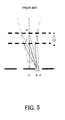
- this interferometer has a problem shown in FIG. 5.
- FIG. 5 is an optical-path diagram for explaining the problem of the system shown in FIG. 4.
- the wave front measurements in the y direction follow the wave front measurements in the x direction. Therefore, the above problem occurs when a position in the optical-axis direction (or z direction) offsets from F to G in FIG. 5 due to stage's driving errors, influence of the vibration, etc., during a replacement of the diffraction grating from B to C.
- the diffraction grating located at the position F causes the wave front to diffract at H and to image at a position J.
- Patrik can avoid this problem, but causes new problems of inevitable optical contrast deteriorations in the signal component and extremely complex signal processing.
- a measuring apparatus includes a first mask having a pinhole for generating a spherical wave as measuring light, a second mask provided subsequent to the first mask in a light traveling direction, the second mask having a selecting window that allows the measuring light that has passed a target optical system to transmit through the selecting window; and a two-dimensional light divider, located between the first and second masks, for two-dimensionally dividing light, wherein the measuring apparatus calculating optical performance of the target optical system from an interference fringe formed by the measuring light that has passed the selecting window.
- the optical performance may be a wave front aberration.
- the measuring apparatus may calculate the optical performance from wave front aberration of the target optical system with respect to two orthogonal directions, wherein the selecting window in the second mask allows ⁇ 1st order diffracted lights of the measuring light in one or both of the two orthogonal directions to simultaneously pass through the selecting window.
- a measuring method includes the steps of dividing measuring light using a two-dimensional divider, obtaining interference information with respect to two orthogonal directions, through a shearing interference between predetermined orders of the measuring lights that have passed a target optical system, a position of the two-dimensional divider being fixed during the obtaining step, the obtaining step using a selecting window plate that has at least two windows aligned with one direction among the two orthogonal directions, and calculating optical performance of the target optical system by integrating the interference information, and by using the interference information of the measuring light that has passed the selecting window plate.
- a measuring method includes the steps of dividing measuring light using a two-dimensional divider, obtaining interference information with respect to two orthogonal directions, through an interference between predetermined orders of the measuring lights that have passed a target optical system, a position of the two-dimensional divider being fixed during the obtaining step, the obtaining step using a selecting window plate that has two pairs of windows aligned with the two orthogonal directions, and calculating optical performance of the target optical system by Fourier-transforming the interference information, by performing spatial frequency filtering for a component of an interference fringe generated by a combination of predetermined openings so as to selectively extract the component, and by using the interference information of the measuring light that has passed the selecting window plate.
- An exposure method includes the steps of calculating optical performance of a target optical system using the above measuring method, adjusting the target optical system based on the optical performance of the target optical system, which is calculated by the calculating step, and exposing an object using the target optical system adjusted by the adjusting step.
- the light may have a wavelength of 20 nm or smaller.
- a device manufacturing method includes the steps of exposing an object to be exposed using the above exposure apparatus, and developing the object exposed. Claims for a device fabricating method for performing operations similar to that of the above exposure apparatus cover devices as intermediate and final products. Such devices include semiconductor chips like an LSI and VLSI, CCDs, LCDs, magnetic sensors, thin film magnetic heads, and the like.
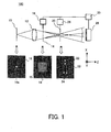
- FIG. 1 shows a basic arrangement of the measuring apparatus 100 according to one embodiment of the present invention.
- the measuring apparatus 100 includes a pinhole plate 10, a target optical system 12, a diffraction grating 14, a stage 16 for the diffraction grating 14, a selecting window plate 20, a stage 26 for the selecting window plate 20, a detector 28, and a controller 30. While FIG. 1 shows the target optical system 12 as a lens, it is a reflection optical system when the exposure apparatus uses the EUV light as a light source.
- the pinhole plate 10 has a pinhole 10a that generates a spherical wave that serves as the measurement light, and is arranged at a desired measurement point on the object surface of the target optical system 12.
- the NA at the illumination optical system side is about 0.0625
- the pinhole plate 10 is illuminated by the illumination optical system (not shown). A high-intensity and high-coherence light source is necessary for the pinhole 10a.
- an undulator radiation X-ray that harrows a band of the X-ray generated from the synchrotron radiation is preferably used.
- the pinhole plate 10 should efficiently shield the EUV light and is made, for example, of Ta and Ni.
- a thickness of the pinhole plate 1 is 200 nm or larger for Ta and 150 nm or larger for Ni.
- the illumination light emitted as a spherical wave from the pinhole 10a passes the target optical system 12 and images on the diffracted light selecting window plate 20.
- the diffracted light selecting window plate 20 has a pair of identically shaped windows 22 aligned with the x direction and another pair of identically shaped windows 24 aligned with the y direction.
- the windows 22 are selected for shearing measurements in the x direction, and positioned so that an image is formed at the center between two windows 22.
- a diffraction grating plate 14 having a two-dimensional diffraction grating 15 is inserted by the stage 16 so that the ⁇ 1st order lights can pass two windows (FIG. 2A). While a shearing ratio between the ⁇ 1st order lights is determined by a window interval, a distance between the diffraction grating 14 and the diffracted light selecting window plate 20, a spatial frequency necessary for the wave front recovery, and the contrast necessary for the interference fringes, the preferable shearing ratio is 1 / 30.
- the selecting window plate 20 is driven to position the 0th order light at the center between the two selecting windows 24. Since the windows 22 and 24 are located on the same mask, an interval between the patterns is adjustable using the electron beam imaging speed, such as about 50 nm, for manufacturing the mask. Moreover, the stage 26 for driving the selecting window plate 20 has the driving precision of about 0.1 ⁇ m even if employing a normal pulsed motor, and the windows 22 and 24 of the selecting window plate 20 have a width of about 1.3 ⁇ m. Therefore, the driving of the stage 26 can provide the sufficient precision for positioning.
- the conventional structure shown in FIG. 4 has difficulties in spatially according the diffraction gratings B and C with the same surface when the windows D and E are exchanged and the diffraction grating B for the x measurements is replaced with the diffraction grating C for the y measurements.
- the measurements errors occur as described above with reference to FIG. 5.
- the instant embodiment does not replace the diffraction grating plate 14 although exchanging the selecting window 20, and thus maintains the highly precise measurements in varying the measurement direction.
- the optical arrangement of the instant embodiment shown in FIG. 1 is distinguished from Patrik's one shown in FIG. 4, in that the instant embodiment changes the diffraction grating from the one-dimensional diffraction gratings B and C to the two-dimensional diffraction grating 15, and includes the selecting window plate 20.
- the detector 28 is a detector or camera that serves as interference fringe observer means, such as a backlight type CCD.
- the controller 30 controls the stages 16 and 26, obtains the shearing interference information detected by the detector 28, conducts the wave front analysis, and calculates the wave front aberration of the target optical system 12.
- the wave front can be restored by introducing the same order diffracted lights to the CCD 28 from the selecting windows 22 and 24 in the similar manner. More specifically, the CCD 28 photographs the independently sheared wave fronts in the x and y components.
- the controller 28 integrates the wave fronts in the shearing direction, and restores the two-dimensional wave front by the path integral.
- the interference fringe image is obtained by scanning the grating in the x direction by 1 / 4 pitch during the x shearing time, and the phase information (or wave front) is calculated by the 5 or 9 bucket method. Since the phase information is discrete information every 360°, unwrapping for smooth phase connections provides the highly precise wave front. These are obtained from the differentiated wave front, and the integral operation restores the original wave front.
- FIG. 3 provides a selecting window plate 20A with two pairs of windows 22A and 24A in the x and y directions.
- the windows 22A correspond to the windows 22, and the windows 24A correspond to the windows 24.
- These two pairs of windows 22A and 24A are arranged at vertexes of a square in FIG. 3.
- the wave front restoration procedure may apply almost the similar approach to Patrik's scheme.
- Patrik's scheme two-dimensionally Fourier-transforms the interference fringes and filters the result so that the interference spectra of the 0th and 1st order lights remain, because the interference contrast between the 0th and 1st order lights is maximum. Since the instant embodiment uses the ⁇ 1st order lights, the filtering leaves twofold spatial frequencies, conducts an inverse Fourier transformation to the result, and extracts the signal component.
- the interference fringe contrast formed by the ⁇ 1st order lights becomes higher by about 10 % than the contrast formed by the 0th and 1st order lights.
- the Patrik's scheme causes the interference fringe between other diffracted orders to deteriorate the signal light contract. Therefore, the present invention can provide more highly precise measurements than Patrik's scheme because the present invention can obtain the higher contrast interference fringes.
- the two-dimensional diffraction grating 15 is fixed when the shearing interference information is obtained in two orthogonal directions, and therefore the measurement error caused by a replacement of the diffraction grating does not occur.
- the instant embodiment calculates the wave front aberration of the target optical system 12 from the shearing interference information directed to the measuring light that has passed through the selecting windows, and facilitates the operation processing because the operation amount is remarkably lower than that in Patrik's scheme.
- FIG. 6 is a schematic block diagram of the exposure apparatus 40 that utilizes the EUV light as the exposure light, although the inventive exposure apparatus is not limited to the EUV light.
- 41 denotes an illumination optical system including the light source
- 42 denotes a reticle stage
- 44 denotes a reticle.
- the reticle 44 may be the first mask 12 or a reticle that has a circuit pattern of a semiconductor device (a semiconductor chip, such as IC and LSI, a liquid crystal panel, and a CCD).
- 12A denotes a projection optical system as a target optical system.
- 45 denotes a wafer stage.
- 14A denotes a diffraction grating plate (or light dividing means). The diffraction grating plate 14A is located at the wafer stage 45 side in FIG. 5, but may be located at the reticle stage 42 side.
- the diffraction grating plate 14A has a similar structure to the diffraction grating plate 14 shown in FIG. 1.
- 46 denotes a pattern surface, on which the windows 22 and 24 are arranged.
- 28 denotes a detector.
- 47 denotes an object to be exposed, which is a wafer in the instant embodiment.
- the pattern surface 46 and the detector 28 are integrated with each other and arranged on the wafer stage 45.
- the illumination optical system 41 illuminates the mask 44, and the diffraction grating 14A divides the wave front that is emitted from the pinhole 10a and spherical in one direction.
- The'projection optical system 12A shields the 0th order light, and allows the ⁇ 1st order diffracted lights to enter the windows 22 (or 22A) and 24 (or 24A), and the detector 28 obtains interference fringes. Since the interference fringes correspond to a differentiation of the original wave front, and the controller obtains the original wave front information by integrating the interference fringes obtained by the detector 28.
- the phase shift means 16 moves the diffraction grating 14A and aberrations are similarly measured at several points in the view angle of the projection optical system 12A.
- This embodiment can easily add an aberration measuring function to the projection exposure apparatus by using a reflection mask pattern.
- the exposure apparatus 40 allows plural optical elements (not shown) in the projection optical system to move in the optical-axis direction and/or a direction orthogonal to the optical-axis direction.
- a driving system not shown
- aberrational adjustments based on aberrational information obtained from the instant embodiment, it is possible to correct or optimize one or more aberrations of the projection optical system, in particular Seidel's classification of aberrations.
- the means for adjusting the aberration of the projection optical system 12A can use various known system, such as a movable lens, a movable mirror (when the projection optical system is a catadioptric optical system or full-mirror optical system), an inclinable parallel plate, a pressure-controllable space, and a surface correction using an actuator.
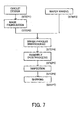
- FIG. 7 is a flowchart for explaining a fabrication of devices (i.e ., semiconductor chips such as IC and LSI, LCDs, CCDs, etc.).
- a fabrication of a semiconductor chip As an example.
- Step 1 circuit design
- Step 2 mask fabrication
- Step 3 wafer making
- Step 4 wafer process
- a pretreatment forms actual circuitry on the wafer through photolithography using the mask and wafer.
- Step 5 (assembly), which is also referred to as a post-treatment, forms into a semiconductor chip the wafer formed in Step 4 and includes an assembly step (e.g., dicing, bonding), a packaging step (chip sealing), and the like.
- Step 6 (inspection) performs various tests for the semiconductor device made in Step 5, such as a validity test and a durability test. Through these steps, a semiconductor device is finished and shipped (Step 7).
- FIG. 8 is a detailed flowchart of the wafer process in Step 4 shown in FIG. 7.
- Step 11 oxidation
- Step 12 CVD
- Step 13 electrode formation
- Step 14 ion implantation
- Step 15 resist process
- Step 16 exposure
- Step 17 development
- Step 18 etching
- Step 19 removes disused resist after etching. These steps are repeated, and multilayer circuit patterns are formed on the wafer 47.
- the manufacturing method of the present invention can manufacture semiconductor devices which have been difficult to manufacture, because the wave front aberration has been corrected with high precision.
- the present invention thus can provide a measuring method and apparatus which utilize the shearing interferometry and provide higher precision and easier signal processing than the conventional method, an exposure method and apparatus using them, and a device manufacturing method.
Landscapes
- Physics & Mathematics (AREA)
- General Physics & Mathematics (AREA)
- Testing Of Optical Devices Or Fibers (AREA)
- Exposure And Positioning Against Photoresist Photosensitive Materials (AREA)
- Exposure Of Semiconductors, Excluding Electron Or Ion Beam Exposure (AREA)
- Instruments For Measurement Of Length By Optical Means (AREA)
Applications Claiming Priority (2)
| Application Number | Priority Date | Filing Date | Title |
|---|---|---|---|
| JP2003398722 | 2003-11-28 | ||
| JP2003398722A JP2005159213A (ja) | 2003-11-28 | 2003-11-28 | シアリング干渉を利用した測定方法及び装置、それを利用した露光方法及び装置、並びに、デバイス製造方法 |
Publications (3)
| Publication Number | Publication Date |
|---|---|
| EP1536287A2 true EP1536287A2 (fr) | 2005-06-01 |
| EP1536287A3 EP1536287A3 (fr) | 2007-09-12 |
| EP1536287B1 EP1536287B1 (fr) | 2011-02-02 |
Family
ID=34463869
Family Applications (1)
| Application Number | Title | Priority Date | Filing Date |
|---|---|---|---|
| EP04028148A Expired - Lifetime EP1536287B1 (fr) | 2003-11-28 | 2004-11-26 | Méthode de mesure et appareil utilisant un interféromètre à décalage, méthode et dispositif d'exposition utilisant ledit appareil, et procédé pour la fabrication d'un dispositif |
Country Status (4)
| Country | Link |
|---|---|
| US (1) | US7352475B2 (fr) |
| EP (1) | EP1536287B1 (fr) |
| JP (1) | JP2005159213A (fr) |
| DE (1) | DE602004031279D1 (fr) |
Cited By (1)
| Publication number | Priority date | Publication date | Assignee | Title |
|---|---|---|---|---|
| US8351050B2 (en) | 2009-01-09 | 2013-01-08 | Canon Kabushiki Kaisha | Wavefront-aberration-measuring device and exposure apparatus |
Families Citing this family (16)
| Publication number | Priority date | Publication date | Assignee | Title |
|---|---|---|---|---|
| JP2008192855A (ja) | 2007-02-05 | 2008-08-21 | Canon Inc | 測定装置、露光装置及びデバイス製造方法 |
| JP2008192936A (ja) * | 2007-02-06 | 2008-08-21 | Canon Inc | 測定装置、露光装置及びデバイス製造方法 |
| JP2009080376A (ja) * | 2007-09-27 | 2009-04-16 | Hitachi Displays Ltd | 液晶表示装置 |
| JP2009253214A (ja) * | 2008-04-10 | 2009-10-29 | Canon Inc | 露光装置及びデバイス製造方法 |
| JP2009277712A (ja) * | 2008-05-12 | 2009-11-26 | Canon Inc | 測定装置および露光装置 |
| DE102008029970A1 (de) * | 2008-06-26 | 2009-12-31 | Carl Zeiss Smt Ag | Projektionsbelichtungsanlage für die Mikrolithographie sowie Verfahren zum Überwachen einer lateralen Abbildungsstabilität |
| JP2010109160A (ja) * | 2008-10-30 | 2010-05-13 | Canon Inc | 測定装置、露光装置及びデバイス製造方法 |
| JP5328437B2 (ja) * | 2009-03-25 | 2013-10-30 | キヤノン株式会社 | 透過波面測定方法、屈折率分布測定方法、光学素子の製造方法、及び透過波面測定装置 |
| US9389519B2 (en) * | 2010-02-25 | 2016-07-12 | Nikon Corporation | Measuring method and measuring apparatus of pupil transmittance distribution, exposure method and exposure apparatus, and device manufacturing method |
| CN102368139B (zh) * | 2011-11-07 | 2013-07-03 | 中国科学院长春光学精密机械与物理研究所 | 一种高精度系统波像差检测方法 |
| US9046791B2 (en) | 2011-11-30 | 2015-06-02 | Changchun Institute Of Optics, Fine Mechanics And Physics, Chinese Academy Of Sciences | Apparatuses and methods for detecting wave front abberation of projection objective system in photolithography machine |
| CN102937513B (zh) * | 2012-11-05 | 2014-11-26 | 上海激光等离子体研究所 | 一种在线监测光栅三维角度扰动的方法和系统 |
| CN103335731B (zh) * | 2013-06-26 | 2015-08-12 | 中国科学院上海光学精密机械研究所 | 光栅剪切波像差检测方法 |
| DE102016212464A1 (de) * | 2016-07-08 | 2018-01-11 | Carl Zeiss Smt Gmbh | Messvorrichtung zum Bestimmen eines Wellenfrontfehlers |
| CN107063477B (zh) * | 2017-03-16 | 2019-04-19 | 中国科学院上海光学精密机械研究所 | 光栅横向剪切干涉大数值孔径波前重建方法 |
| EP3498170A1 (fr) * | 2017-12-12 | 2019-06-19 | Koninklijke Philips N.V. | Dispositif et procédé permettant d'aligner une diffraction de rayons x à une source de rayonnement de rayons x et système d'acquisition d'image à rayons x |
Citations (3)
| Publication number | Priority date | Publication date | Assignee | Title |
|---|---|---|---|---|
| WO2002012826A1 (fr) | 2000-08-04 | 2002-02-14 | The Regents Of The University Of California | Interferometre de cisaillement lateral double domaine |
| JP2003086501A (ja) | 2001-07-04 | 2003-03-20 | Nikon Corp | 波面収差計測機 |
| US6573997B1 (en) | 2000-07-17 | 2003-06-03 | The Regents Of California | Hybrid shearing and phase-shifting point diffraction interferometer |
Family Cites Families (19)
| Publication number | Priority date | Publication date | Assignee | Title |
|---|---|---|---|---|
| DE69129732T2 (de) | 1990-11-30 | 1998-12-17 | Canon K.K., Tokio/Tokyo | Verfahren zur Positionsdetektion |
| JPH0540013A (ja) | 1991-08-05 | 1993-02-19 | Canon Inc | ずれ測定方法及びこの方法を用いた露光装置 |
| US5495336A (en) | 1992-02-04 | 1996-02-27 | Canon Kabushiki Kaisha | Position detecting method for detecting a positional relationship between a first object and a second object |
| JP3008654B2 (ja) | 1992-02-21 | 2000-02-14 | キヤノン株式会社 | 位置検出装置 |
| JP3428705B2 (ja) | 1993-10-20 | 2003-07-22 | キヤノン株式会社 | 位置検出装置及びそれを用いた半導体素子の製造方法 |
| JPH07135168A (ja) | 1993-11-11 | 1995-05-23 | Canon Inc | アライメント方法及びそれを用いた位置検出装置 |
| US5777744A (en) | 1995-05-16 | 1998-07-07 | Canon Kabushiki Kaisha | Exposure state detecting system and exposure apparatus using the same |
| JP3269343B2 (ja) | 1995-07-26 | 2002-03-25 | キヤノン株式会社 | ベストフォーカス決定方法及びそれを用いた露光条件決定方法 |
| JP3517504B2 (ja) | 1995-12-15 | 2004-04-12 | キヤノン株式会社 | 位置検出装置及びそれを用いたデバイスの製造方法 |
| JPH09210629A (ja) | 1996-02-02 | 1997-08-12 | Canon Inc | 面位置検出装置及びそれを用いたデバイスの製造方法 |
| US5969820A (en) | 1996-06-13 | 1999-10-19 | Canon Kabushiki Kaisha | Surface position detecting system and exposure apparatus using the same |
| JP4136067B2 (ja) | 1997-05-02 | 2008-08-20 | キヤノン株式会社 | 検出装置及びそれを用いた露光装置 |
| JPH11265847A (ja) | 1998-01-16 | 1999-09-28 | Canon Inc | 位置検出方法及び位置検出装置 |
| US6307635B1 (en) * | 1998-10-21 | 2001-10-23 | The Regents Of The University Of California | Phase-shifting point diffraction interferometer mask designs |
| JP4846888B2 (ja) | 1998-12-01 | 2011-12-28 | キヤノン株式会社 | 位置合わせ方法 |
| DE10260985A1 (de) | 2002-12-18 | 2004-05-13 | Carl Zeiss Smt Ag | Vorrichtung zur interferometrischen Wellenfrontvermessung eines optischen Abbildungssystems |
| JP4266673B2 (ja) * | 2003-03-05 | 2009-05-20 | キヤノン株式会社 | 収差測定装置 |
| JP2005156403A (ja) * | 2003-11-27 | 2005-06-16 | Canon Inc | シアリング干渉を利用した測定方法及び装置、それを利用した露光方法及び装置、並びに、デバイス製造方法 |
| JP2006228930A (ja) * | 2005-02-17 | 2006-08-31 | Canon Inc | 測定装置及びそれを搭載した露光装置 |
-
2003
- 2003-11-28 JP JP2003398722A patent/JP2005159213A/ja active Pending
-
2004
- 2004-11-23 US US10/994,314 patent/US7352475B2/en not_active Expired - Fee Related
- 2004-11-26 EP EP04028148A patent/EP1536287B1/fr not_active Expired - Lifetime
- 2004-11-26 DE DE602004031279T patent/DE602004031279D1/de not_active Expired - Lifetime
Patent Citations (3)
| Publication number | Priority date | Publication date | Assignee | Title |
|---|---|---|---|---|
| US6573997B1 (en) | 2000-07-17 | 2003-06-03 | The Regents Of California | Hybrid shearing and phase-shifting point diffraction interferometer |
| WO2002012826A1 (fr) | 2000-08-04 | 2002-02-14 | The Regents Of The University Of California | Interferometre de cisaillement lateral double domaine |
| JP2003086501A (ja) | 2001-07-04 | 2003-03-20 | Nikon Corp | 波面収差計測機 |
Non-Patent Citations (3)
| Title |
|---|
| K. MURAKAMI ET AL., PROCEEDINGS OF SPIE, vol. 5037, 2003, pages 257 - 264 |
| P. NAULLEAU ET AL., J. VAC. SCI. TECHNOL. B, vol. 18, no. 6, 2000, pages 2939 - 2943 |
| Y. ZHU ET AL., JPN. J. APPL. PHYS., vol. 42, 2003, pages 5844 - 5847 |
Cited By (1)
| Publication number | Priority date | Publication date | Assignee | Title |
|---|---|---|---|---|
| US8351050B2 (en) | 2009-01-09 | 2013-01-08 | Canon Kabushiki Kaisha | Wavefront-aberration-measuring device and exposure apparatus |
Also Published As
| Publication number | Publication date |
|---|---|
| US7352475B2 (en) | 2008-04-01 |
| US20050117170A1 (en) | 2005-06-02 |
| DE602004031279D1 (de) | 2011-03-17 |
| JP2005159213A (ja) | 2005-06-16 |
| EP1536287A3 (fr) | 2007-09-12 |
| EP1536287B1 (fr) | 2011-02-02 |
Similar Documents
| Publication | Publication Date | Title |
|---|---|---|
| KR100562190B1 (ko) | 리소그래피장치의 투영시스템의 수차를 측정하는 방법,디바이스제조방법, 및 그 제조된 디바이스 | |
| JP4222926B2 (ja) | デバイス検査 | |
| EP1536287B1 (fr) | Méthode de mesure et appareil utilisant un interféromètre à décalage, méthode et dispositif d'exposition utilisant ledit appareil, et procédé pour la fabrication d'un dispositif | |
| JP5219534B2 (ja) | 露光装置及びデバイスの製造方法 | |
| US7724376B2 (en) | Wavefront-aberration measuring method and device, and exposure apparatus including the device | |
| KR20220016950A (ko) | 계측 방법 및 연관된 계측, 그리고 리소그래피 장치 | |
| EP1568976B1 (fr) | Appareil d'exposition équipé d'un dispositif de mesure | |
| WO2010134487A1 (fr) | Procédé et dispositif de mesure de front d'onde et procédé et dispositif d'exposition | |
| KR100911223B1 (ko) | 측정장치, 노광장치 및 방법, 그리고 디바이스의 제조방법 | |
| NL2014956A (en) | Lithographic Method and Apparatus. | |
| JP2007234685A (ja) | 測定装置、当該測定装置を有する露光装置及びデバイス製造方法 | |
| JP2002206990A (ja) | 波面収差測定方法及び投影露光装置 | |
| US7253907B2 (en) | Measuring method and apparatus using shearing interferometry, exposure method and apparatus using the same, and device manufacturing method | |
| JP2006324311A (ja) | 波面収差測定装置及びそれを有する露光装置 | |
| JP2011142279A (ja) | 波面収差計測方法及び装置、並びに露光方法及び装置 | |
| US20060061757A1 (en) | Method of calculating two-dimensional wavefront aberration | |
| US7889315B2 (en) | Lithographic apparatus, lens interferometer and device manufacturing method | |
| JP4280521B2 (ja) | 収差測定装置及び投影露光装置 | |
| KR101019767B1 (ko) | 노광장치 및 디바이스 제조방법 | |
| JP4724558B2 (ja) | 測定方法及び装置、露光装置 | |
| JP4731951B2 (ja) | 干渉縞の解析方法及び装置、測定装置、露光装置及びデバイス製造方法 | |
| EP1538483B1 (fr) | Méthode et dispositif pour la mesure, méthode et appareil d'exposition et méthode de fabrication d'un dispositif | |
| JP4590181B2 (ja) | 測定方法及び装置、露光装置、並びに、デバイス製造方法 | |
| JP2003178968A (ja) | 収差計測方法及び投影露光装置 | |
| JP2025522545A (ja) | 物理量を決定する方法および装置 |
Legal Events
| Date | Code | Title | Description |
|---|---|---|---|
| PUAI | Public reference made under article 153(3) epc to a published international application that has entered the european phase |
Free format text: ORIGINAL CODE: 0009012 |
|
| AK | Designated contracting states |
Kind code of ref document: A2 Designated state(s): AT BE BG CH CY CZ DE DK EE ES FI FR GB GR HU IE IS IT LI LU MC NL PL PT RO SE SI SK TR |
|
| AX | Request for extension of the european patent |
Extension state: AL HR LT LV MK YU |
|
| PUAL | Search report despatched |
Free format text: ORIGINAL CODE: 0009013 |
|
| AK | Designated contracting states |
Kind code of ref document: A3 Designated state(s): AT BE BG CH CY CZ DE DK EE ES FI FR GB GR HU IE IS IT LI LU MC NL PL PT RO SE SI SK TR |
|
| AX | Request for extension of the european patent |
Extension state: AL HR LT LV MK YU |
|
| 17P | Request for examination filed |
Effective date: 20080312 |
|
| AKX | Designation fees paid |
Designated state(s): DE NL |
|
| 17Q | First examination report despatched |
Effective date: 20080505 |
|
| GRAJ | Information related to disapproval of communication of intention to grant by the applicant or resumption of examination proceedings by the epo deleted |
Free format text: ORIGINAL CODE: EPIDOSDIGR1 |
|
| GRAP | Despatch of communication of intention to grant a patent |
Free format text: ORIGINAL CODE: EPIDOSNIGR1 |
|
| GRAP | Despatch of communication of intention to grant a patent |
Free format text: ORIGINAL CODE: EPIDOSNIGR1 |
|
| GRAS | Grant fee paid |
Free format text: ORIGINAL CODE: EPIDOSNIGR3 |
|
| GRAA | (expected) grant |
Free format text: ORIGINAL CODE: 0009210 |
|
| AK | Designated contracting states |
Kind code of ref document: B1 Designated state(s): DE NL |
|
| REF | Corresponds to: |
Ref document number: 602004031279 Country of ref document: DE Date of ref document: 20110317 Kind code of ref document: P |
|
| REG | Reference to a national code |
Ref country code: DE Ref legal event code: R096 Ref document number: 602004031279 Country of ref document: DE Effective date: 20110317 |
|
| REG | Reference to a national code |
Ref country code: NL Ref legal event code: T3 |
|
| PLBE | No opposition filed within time limit |
Free format text: ORIGINAL CODE: 0009261 |
|
| STAA | Information on the status of an ep patent application or granted ep patent |
Free format text: STATUS: NO OPPOSITION FILED WITHIN TIME LIMIT |
|
| 26N | No opposition filed |
Effective date: 20111103 |
|
| REG | Reference to a national code |
Ref country code: DE Ref legal event code: R097 Ref document number: 602004031279 Country of ref document: DE Effective date: 20111103 |
|
| PGFP | Annual fee paid to national office [announced via postgrant information from national office to epo] |
Ref country code: NL Payment date: 20171124 Year of fee payment: 14 |
|
| PGFP | Annual fee paid to national office [announced via postgrant information from national office to epo] |
Ref country code: DE Payment date: 20180131 Year of fee payment: 14 |
|
| REG | Reference to a national code |
Ref country code: DE Ref legal event code: R119 Ref document number: 602004031279 Country of ref document: DE |
|
| REG | Reference to a national code |
Ref country code: NL Ref legal event code: MM Effective date: 20181201 |
|
| PG25 | Lapsed in a contracting state [announced via postgrant information from national office to epo] |
Ref country code: NL Free format text: LAPSE BECAUSE OF NON-PAYMENT OF DUE FEES Effective date: 20181201 |
|
| PG25 | Lapsed in a contracting state [announced via postgrant information from national office to epo] |
Ref country code: DE Free format text: LAPSE BECAUSE OF NON-PAYMENT OF DUE FEES Effective date: 20190601 |