EP1535328B1 - Circuit integre avec couche de metallisation comportant des materiaux intermediaires - Google Patents
Circuit integre avec couche de metallisation comportant des materiaux intermediaires Download PDFInfo
- Publication number
- EP1535328B1 EP1535328B1 EP03794790.0A EP03794790A EP1535328B1 EP 1535328 B1 EP1535328 B1 EP 1535328B1 EP 03794790 A EP03794790 A EP 03794790A EP 1535328 B1 EP1535328 B1 EP 1535328B1
- Authority
- EP
- European Patent Office
- Prior art keywords
- interconnect
- connecting section
- intermediate material
- constriction
- dielectric
- Prior art date
- Legal status (The legal status is an assumption and is not a legal conclusion. Google has not performed a legal analysis and makes no representation as to the accuracy of the status listed.)
- Expired - Lifetime
Links
Images



Classifications
-
- H—ELECTRICITY
- H10—SEMICONDUCTOR DEVICES; ELECTRIC SOLID-STATE DEVICES NOT OTHERWISE PROVIDED FOR
- H10W—GENERIC PACKAGES, INTERCONNECTIONS, CONNECTORS OR OTHER CONSTRUCTIONAL DETAILS OF DEVICES COVERED BY CLASS H10
- H10W20/00—Interconnections in chips, wafers or substrates
- H10W20/40—Interconnections external to wafers or substrates, e.g. back-end-of-line [BEOL] metallisations or vias connecting to gate electrodes
- H10W20/41—Interconnections external to wafers or substrates, e.g. back-end-of-line [BEOL] metallisations or vias connecting to gate electrodes characterised by their conductive parts
- H10W20/42—Vias, e.g. via plugs
-
- G—PHYSICS
- G06—COMPUTING OR CALCULATING; COUNTING
- G06F—ELECTRIC DIGITAL DATA PROCESSING
- G06F30/00—Computer-aided design [CAD]
- G06F30/30—Circuit design
- G06F30/39—Circuit design at the physical level
-
- H—ELECTRICITY
- H10—SEMICONDUCTOR DEVICES; ELECTRIC SOLID-STATE DEVICES NOT OTHERWISE PROVIDED FOR
- H10W—GENERIC PACKAGES, INTERCONNECTIONS, CONNECTORS OR OTHER CONSTRUCTIONAL DETAILS OF DEVICES COVERED BY CLASS H10
- H10W20/00—Interconnections in chips, wafers or substrates
- H10W20/01—Manufacture or treatment
- H10W20/031—Manufacture or treatment of conductive parts of the interconnections
- H10W20/032—Manufacture or treatment of conductive parts of the interconnections of conductive barrier, adhesion or liner layers
-
- H—ELECTRICITY
- H10—SEMICONDUCTOR DEVICES; ELECTRIC SOLID-STATE DEVICES NOT OTHERWISE PROVIDED FOR
- H10W—GENERIC PACKAGES, INTERCONNECTIONS, CONNECTORS OR OTHER CONSTRUCTIONAL DETAILS OF DEVICES COVERED BY CLASS H10
- H10W20/00—Interconnections in chips, wafers or substrates
- H10W20/40—Interconnections external to wafers or substrates, e.g. back-end-of-line [BEOL] metallisations or vias connecting to gate electrodes
- H10W20/41—Interconnections external to wafers or substrates, e.g. back-end-of-line [BEOL] metallisations or vias connecting to gate electrodes characterised by their conductive parts
- H10W20/425—Barrier, adhesion or liner layers
-
- H—ELECTRICITY
- H10—SEMICONDUCTOR DEVICES; ELECTRIC SOLID-STATE DEVICES NOT OTHERWISE PROVIDED FOR
- H10W—GENERIC PACKAGES, INTERCONNECTIONS, CONNECTORS OR OTHER CONSTRUCTIONAL DETAILS OF DEVICES COVERED BY CLASS H10
- H10W20/00—Interconnections in chips, wafers or substrates
- H10W20/40—Interconnections external to wafers or substrates, e.g. back-end-of-line [BEOL] metallisations or vias connecting to gate electrodes
- H10W20/41—Interconnections external to wafers or substrates, e.g. back-end-of-line [BEOL] metallisations or vias connecting to gate electrodes characterised by their conductive parts
- H10W20/435—Cross-sectional shapes or dispositions of interconnections
Definitions
- the interconnect intermediate material touches at at least one connection at opposite edges of the interconnect.
- the contact of the intermediate materials produces a current path redundancy which, even with constant electromigration, enables a longer operation of the integrated circuit arrangement.
- the interconnect intermediate material at the connection contacts the connecting section intermediate material at three side surfaces or edges of a conductive path.
- the current conductivity is markedly higher compared to arrangements without a contact point or with fewer contact areas or a small contact area of connecting section intermediate material and interconnect material.
- the reason for this is the "barrier redundancy".
- the interconnect at the connecting portion has a constriction whose width is selected in one embodiment so that arise on opposite side surfaces of the interconnect contact areas.
- the constriction can be comparatively short in comparison to the total length of a conductor track.
- the constriction has a length which is less than five times or even less than three times the width of the constriction at its narrowest point. Using constrictions is an easy way to increase the number of contact areas of the intermediate materials.
- the connecting section is arranged at the end of the conductor track.
- the constriction has the shape of a wedge or the shape of a step.
- the interconnect extends from the connection section out in at least two different directions.
- the constriction has at its ends in each case the shape of a wedge or the shape of a step.
- FIG. 1 shows a section of an integrated circuit 10, which includes a via 12 and a conductive line 14.
- the integrated circuit 10 includes design data that has not yet been processed by a method of selectively increasing the number of touches of liners.
- the integrated circuit 10 includes a metallization layer 16 extending substantially in a plane parallel to the surface of a semiconductor substrate, not shown, in which a plurality of semiconductor integrated devices are arranged, e.g. FET transistors (Field Effect Transistor).
- a plurality of semiconductor integrated devices are arranged, e.g. FET transistors (Field Effect Transistor).
- FET transistors Field Effect Transistor
- a plurality of other interconnects, not shown are included, which are separated from one another by a dielectric 18, for example by silicon dioxide.
- the interconnects 14 of the metallization layer 16 are made of copper.
- the metallization layer 16 is covered by a dielectric intermediate layer 22, for example of silicon nitride.
- a dielectric layer 24 for example of silicon dioxide, in which a multiplicity of vias are arranged, for example the via 12.
- first contact holes 26 were etched into the dielectric layer 24 and the interlayer dielectric layer 22.
- a via-liner layer was deposited, with, for example, a via liner 28 having been deposited in the contact hole 26.
- the via liner 28 also covers the bottom 30 of the contact hole 26.
- the bottom 30 of the contact hole 26 lies directly on a top surface of the guide track 14 or penetrates slightly into the guide track 14.
- the via liner 28 has the same thickness as the leader liner 20.
- the liner material for the leader liner 20 and for the via liner 28 is titanium nitride.
- the contact holes 26 were filled, for example, with tungsten or copper, whereby the via 12 has been produced.
- the dielectric layer 24 are in the embodiment even more metallization.
- a coordinate system 32 is shown having an x-axis 34, a y-axis 36 and a z-axis 38.
- the xy plane is parallel to the planes in which the metallization layer 16, the dielectric intermediate layer 22 and the dielectric layer 24 lie.
- the z-direction coincides with the direction in which the metallization layer 16, the interlayer dielectric layer 22, and the dielectric layer 24 are stacked one over the other.
- the z-direction coincides with the direction of a normal of the surface of the semiconductor substrate.
- the via 12 can be offset in the y-direction to the upper edge of a rear side surface 40 of the guide track 14, so that there is a contact point on an edge 42 of the guide track 14.
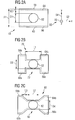
- FIG. 2A shows a plan view on two levels of a design 48 of the patterns of two masks for fabricating an integrated circuit, and ultimately also for structures in two levels of the integrated circuit itself.
- a coordinate system 50 is the reference for design data for defining the designs and applies to the designs of FIGS. 2A to 3C ,
- the coordinate system 50 has an x-axis 52, a y-axis 54, and a z-axis 56.
- the designs are each in an xy plane.
- the coordinate system 50 has the same position with respect to the designs as the coordinate system 32 with respect to the integrated circuit arrangement 10.
- a design plane for the location of mask patterns for the creation of interconnect trenches in a metallization layer is located opposite to the z-direction below a design plane for the location of mask patterns for creating via vias.
- the position of edges of the trenches is specified by means of straight lines or lines in the lower design plane.
- the location of the edges of contact holes is given by circles in the upper plane of the design, see, for example, the lines 58 and 60 for specifying the position of the edge of a track and a circle 62 for specifying the position of a contact hole leading to the track.
- a width B1 between the mutually parallel straight lines 58 and 60 establishes the width of a trench for the interconnect, taking into account a scaling factor.
- a diameter D1 of the circle 62 determines the diameter of the contact hole, taking into account the scaling factor.
- the width B1 in the design is about twice as large as the diameter D1.
- the circle 62 is centered between the two straight lines 60 and 58.
- a width B2 is shown, which corresponds to the width of the conductor track liner, taking into account the scaling factor.
- the width B2 is for example one-tenth of the width B1.
- Dashed lines 64 and 66 indicate the location of the inner edge of the track liner with respect to the design 48.
- FIG. 2B shows a design 70, from the on hand of the FIG. 2A explained design with the help of a below at hand of FIG. 8 explained in more detail method has been generated automatically.
- design 70 there is a constriction 72 along lines 58a and 60a corresponding to lines 58 and 60.
- the constriction 72 is located below the circle 62, whose Location and diameter D1 has remained unchanged.
- At the ends of the constriction 72 are steps.
- the constriction 72 has a length L1 that is about twice as large as the diameter D1 of the circle 62.
- the constriction 72 has a uniform width B3.
- the width B3 of the constriction 72 is equal to the diameter D1. In another embodiment, the width B3 is even smaller than the diameter D1.
- the circle 62 is centered on the steps at the end of the constriction 72. This occurs in areas which later have the same position in the integrated circuit, such as overlapping areas between the circle 62 and the gap between the lines 58a and 64a or between the lines 60a and 66a to a contact of the conductor track liner and the via line. Liners. Dashed lines 64a and 66a correspond to dashed lines 64 and 66 and indicate the location of the track liner with respect to the design 70.
- FIG. 2C shows an alternative change of the design data according to FIG. 2A
- a constriction 82 having wedge-shaped ends has been created.
- the location and the diameter of the circle 62 have remained unchanged.
- the location of lines 58 and 60 has been changed by simple geometrical calculations to produce lines 58b and 60b forming the constriction 82.
- the course of the lines 58b and 60b coincides with the course of the lines 58 and 60.
- the lines 58b and 60b first approach each other continuously within a length L3 which is slightly smaller than the diameter D1 of the circle 62. For example, if the interconnect more than three times as wide as the diameter of the vias, so in another embodiment, the length L3 is greater than D1.
- the lines 58b and 60b run parallel to each other for a length L2.
- the Length L2 has a value which is about one and a half times the value of the diameter D1.
- lines 58b and 60b again diverge within a length L3. Due to the constriction 82, overlapping areas again arise between the circle 62 and the space between the line 58b and a dashed line 64b and between the line 60B and a dashed line 66b. Dashed lines 64b and 66b represent the location of the track liner with respect to design 80.
- FIG. 3A shows a design 90 with U-shaped lines 92, 94 and 96 in a first plane of design and with a circle 98 surrounded by the lines 92 to 96 overlapping circle 98.
- the lines 92 to 96 ultimately define the position of the edges of trenches for a Track firmly.
- the circle 98 ultimately determines the position of a contact hole, which leads to the interconnect.
- a width B5 between two mutually parallel straight lines 92 and 96 establishes the width of the trench, taking into account the scaling factor.
- the diameter D2 of the circle 98 determines the diameter of the contact hole, taking into account the scaling factor.
- the width B5 is about twice as large as the diameter D2.
- a dashed line 100 serves to illustrate the position of the inner edge of the interconnect liner layer.
- the line 100 has a distance B6 to the line 92, 94 and 96, which is for example about one-tenth of the width B5.
- FIG. 3B shows a design 110, with the help of the bottom of the hand FIG. 8 explained method automatically from the based on FIG. 3A explained design has been generated.
- the straight lines 92, 94 and 96 in the design 90 correspond in design to 110 lines 114, 116 and 118.
- the constriction 112 is defined by the symmetrical lines 114 and 118 118 formed and has stepped ends.
- the constriction 112 has at its narrowest point a width B7 which coincides with the diameter D2 of the circle 98.
- a length L4 of the constriction 112 is about one and a half times the diameter D2.
- the location of circle 98 in design 110 has remained unchanged with respect to the location of circle 98 in design 90. This means that the end face of the conductor track defined by the straight line 94 has been offset somewhat in the opposite direction of the x-direction 52.
- FIG. 3C shows a design 130 which, when using an alternative rule, is described below with reference to FIG FIG. 8 explained method from the on hand of the FIG. 3A illustrated design 90 has been generated.
- the location of the circle 98 and its diameter D2 have remained unchanged.
- a line 132 has been created on the lines 92-96 of corresponding lines 134, 136, and 138.
- the constriction 132 has a wedge-shaped portion with a length L5.
- the value of the length L6 is about one fifth larger than the value of the diameter D2.
- the length is L5 about half the diameter D2 of the circle 98.
- a width B8 of the constriction 132 at its narrowest point is equal to the diameter D2.
- FIG. 4A shows a non-inventive design 150 with a straight line 152, which ultimately determines the position of the edge of a trench for a track.
- a dashed line 154 illustrates the position of a conductor track liner.
- a circle 156 belongs to a different design plane and specifies the position of a contact hole leading to the interconnect. The circle 156 has a distance to the straight line 152, in which no overlap of the circle 156 with the straight line 152 or with the straight line 154 occurs.
- a coordinate system 160 having an x-axis 162, a y-axis 164 and a z-axis 166 is valid.
- the position of design planes and coordinate system 160 what has been said about the coordinate system 50 applies.
- FIG. 4B shows a non-inventive design 170, which from the draft 150 with the aid of the bottom of the FIG. 8 explained method has been generated automatically.
- the location of lines 152 and 154 has not changed.
- a circle 156a has been displaced in the y-direction compared to the circle 156 so that its edge has a largest y-coordinate, which coincides with the y-coordinate of the line 152.
- Due to the offset circle 156a there is an overlap area 172 where the circle 156a overlaps the space between the straight line 152 and the dashed straight line 154. This overlap results in overlap of the interconnect liner with the via liner in a interconnect pad assembly made according to design 170.
- FIG. 5A shows a non-inventive design 180 for the arrangement of a contact hole represented by a circle 182 at the end of a pattern formed by U-shaped lines 184, 186 and 188 pattern.
- the circle 182 is located in the middle of a region enclosed by the straight lines 184 to 188 and has a diameter D4 which is about one-third smaller than a distance B of the mutually parallel lines 184 and 188 corresponding width B9 of the sample.
- D4 diameter of the circle 182 and a dashed line 190 representing the location of the track liner.
- FIG. 5B shows a design 200, not according to the invention, automatically generated from the design 180.
- the position of the lines 184 to 188 has remained unchanged.
- the circle 182 has been displaced in the x-direction so that a circle 182a has emerged.
- the largest x coordinate of the circle 182a coincides with the x coordinate of the line 186, which indicates the location of the face of the pattern.
- An overlap area 202 is formed between the circle 182a and the area lying between the dashed line 190 and the line 186.
- FIG. 5C shows a non-inventive design 210, which has been automatically generated from the design 180 in an alternative method.
- the position of the lines 184, 186 and 188 has remained unchanged.
- the circle 182 has been displaced both in the x-direction and in the y-direction, so that a circle 182b has arisen.
- the largest x-coordinate of the circle 182b coincides with the x-coordinate of the line 186.
- the largest y-coordinate of the circle 182b coincides with the y-coordinate of the line 184.
- the design 214 has been created by successively applying rules for shifting the circle 182 in the x-direction and in the y-direction.
- FIG. 6A shows a design not according to the invention 220, the U-shaped arranged lines 222, 224 and 226, which ultimately dictate the position of the edge of a trench for a track.
- a distance between the mutually parallel straight lines 222 and 226 defines a width B10 of the pattern formed by the straight lines 222, 224 and 226.
- the design 220 includes a circle 228 which ultimately defines the location of a contact hole.
- a dashed line 230 shows the location of a track liner with respect to the design 220.
- the circle 228 is the area between the line 222 and the dashed line 230 and between the line, respectively 226 and the dashed line 230 overlaps.
- the circle 232 has a diameter D5 equal to the width B10.
- FIG. 6B shows an automatically generated from the draft 220 design not 240 according to the invention.
- the position of the lines 222 to 226 has remained unchanged.
- the circle 228 has been displaced in the x-direction, resulting in a circle 228a.
- the largest x-coordinate of the circle 228a coincides with the x-coordinate of the line 224.
- FIG. 7 shows a non-inventive design 250 in which there are four overlap regions 252, 254, 256 and 258 of a circle 260 with regions between the square forming lines 262, 264, 266 and 268 and a dashed line 270.
- the circle 260 has a diameter D6.
- the square has a side length B11 and B12, which is equal to the diameter D6.
- the method step 314 also follows immediately after the method step 308 if it is determined in this method step 308 that no change according to a rule is possible.
- method step 314 it is checked whether there are more unprocessed contact points according to the original design data. If this is the case, method step 306 follows immediately after method step 314. Thus, the method is located in a process loop from method steps 306 to 314. When method steps 308 to 314 are carried out in this method loop, all the contact points of the design gradually become and, where appropriate, modify the design data for the contact points in accordance with the rules laid down. The loop from method steps 308 to 314 is only left in method step 314 if there are no further contact points according to the design which have not yet been checked and if necessary have been changed. In this case, a method step 316 follows immediately after method step 314.
- the changed design data are stored in a file and are thus available for further processing, for example for production of masks for producing the integrated circuit arrangement.
- the modified design data is output, for example as a graphical representation on a screen.
- a developer now has the opportunity to test samples of the changes made.
- the method is ended in a method step 318.
- FIG. 9 shows a device 320 for performing the on the basis of FIG. 8
- the method 320 includes a design data specification unit 322, a rule specification unit 324, a control unit 326, a change unit 328, and a memory unit 330, eg, a RAM (Random Access Memory).
- the default units 322 and 324, the control unit 326 and the changing unit 328 access the memory unit 330 via a memory bus 332.
- the control unit 326 controls the operations in the default unit 322, in the default unit 324 and in the change unit 328, see arrows 334 to 338.
- the specification unit 322 is used to specify the design data, that is to say, to carry out the method step 302.
- the specification unit 324 is used to store rules, ie to execute the method step 304.
- the modification unit 328 serves to change the design data according to the rules specified by the predefined unit 324.
- An input unit 340, eg a keyboard, an output unit 342, eg a screen, and a floppy disk drive 344 are also connected to the device 320 via a line 346, 348 or 350.
- the functions of the units 322 through 328 are provided by electronic switching devices that do not include a processor.
- the functions of the units 322-328 are provided by means of a processor 352 which is a program in a program memory unit processed in a program memory unit 354, see arrow 356.
Landscapes
- Engineering & Computer Science (AREA)
- Computer Hardware Design (AREA)
- Physics & Mathematics (AREA)
- Theoretical Computer Science (AREA)
- Evolutionary Computation (AREA)
- Geometry (AREA)
- General Engineering & Computer Science (AREA)
- General Physics & Mathematics (AREA)
- Design And Manufacture Of Integrated Circuits (AREA)
- Internal Circuitry In Semiconductor Integrated Circuit Devices (AREA)
- Electrodes Of Semiconductors (AREA)
- Coupling Device And Connection With Printed Circuit (AREA)
Claims (8)
- Circuit (10) intégré,
comprenant au moins une couche (16) de métallisation, qui comporte une pluralité de pistes (14) conductrices de l'électricité,
comprenant un diélectrique (18) de piste conductrice entre les pistes (14) conductrices, comprenant du matériau (20) intermédiaire de piste conductrice conducteur de l'électricité, disposé respectivement entre une surface (40) latérale d'une piste (14) conductrice et le diélectrique (16) de piste conductrice,
comprenant une pluralité de tronçons (12) de liaison conducteurs de l'électricité, qui forment chacun un tronçon d'une liaison conductrice d'électricité allant à une piste (14) conductrice ou en partant,
comprenant un diélectrique (24) de tronçon de liaison entre les tronçons (12) de liaison,
comprenant du matériau (28) intermédiaire de tronçon de liaison disposé respectivement entre un tronçon (12) de liaison et le diélectrique (24) de tronçon de liaison et/ou entre un tronçon (12) de liaison et une piste (14) conductrice,
dans lequel, sur au moins un tronçon (12) de liaison, le matériau (20) intermédiaire de piste conductrice et le matériau (28) intermédiaire de tronçon de liaison se touchent l'un l'autre en des zones de contact et produisent ainsi une redondance de trajet de courant,
dans lequel la pise (14) conductrice a, sur le tronçon (12) de liaison, un amincissement (72, 82, 112, 132), dont la largeur (B3, B4, B7, B8) est choisie, de manière à créer les zones de contact sur des surfaces latérales opposées de la piste (14) conductrice. - Circuit (10) intégré suivant la revendication 1, dans lequel l'amincissement (72, 112) a, le long de l'axe longitudinal de la piste (14) conductrice, une longueur (L1, L2), qui est plus petite que le cinquième, ou plus petite que le triple de la largeur (B3, B7) de l'amincissement (72, 112).
- Circuit (10) intégré suivant la revendication 1 ou 2, caractérisé en ce que, sur la liaison, le matériau (20) intermédiaire de piste conductrice et le matériau (28) intermédiaire de tronçon de liaison se touchent sur trois surfaces (40) latérales d'une piste (14) conductrice et/ou en ce que le matériau (20) intermédiaire de piste conductrice et le matériau (28) intermédiaire de tronçon de liaison se touchent sur un bord (42) formé par la ligne de contact de deux surfaces latérales de la piste (14) conductrice.
- Circuit (10) intégré suivant l'une des revendications précédentes, caractérisé en ce que le tronçon (12) de liaison est disposé à l'extrémité de la piste (14) conductrice.
- Circuit (10) intégré suivant l'une des revendications précédentes, caractérisé en ce que l'amincissement (112, 132) a la forme d'un coin ou la forme d'un gradin.
- Circuit (10) intégré suivant l'une des revendications 1 à 3, caractérisé en ce que la piste (14) conductrice s'étend à partir du tronçon (12) de liaison dans au moins deux directions différentes,
et/ou en ce que l'amincissement (72, 82) a, à ses extrémités, respectivement la forme d'un coin ou la forme d'un gradin. - Circuit (10) intégré suivant l'une des revendications précédentes, caractérisé en ce que la piste (14) conductrice est en cuivre ou en un alliage de cuivre, qui contient au moins quatre-vingt-quinze pourcent de cuivre,
et/ou en ce que la piste (14) conductrice est en aluminium ou en un alliage d'aluminium, qui contient au moins quatre-vingt-quinze pourcent d'aluminium,
et/ou en ce que le diélectrique (18) de piste conductrice et/ou le diélectrique de tronçon de liaison contient un oxyde, de préférence du dioxyde de silicium ou un diélectrique ayant une constante diélectrique plus petite que 3,9,
et/ou en ce que le matériau (20) intermédiaire de piste conductrice et/ou le matériau (28) intermédiaire de tronçon de liaison contient un nitrure, en étant de préférence constitué d'un nitrure, notamment d'un nitrure métallique,
et/ou en ce que le matériau intermédiaire de piste conductrice contient un métal réfractaire ou est constitué d'un métal réfractaire, en étant de préférence en tantale,
et/ou en ce que les tronçons (12) de liaison contiennent du tungstène, en étant constitué de préférence en tungstène, ou en ce que les tronçons (12) de liaison contiennent du cuivre ou sont constitués de cuivre. - Circuit (10) intégré suivant l'une des revendications précédentes, caractérisé en ce que les surfaces, voisines d'un tronçon (12) de liaison, d'une piste (14) conductrice, sont sensiblement exempts et/ou exempts à plus de quatre-vingt pourcent d'un matériau intermédiaire conducteur de l'électricité.
Priority Applications (2)
| Application Number | Priority Date | Filing Date | Title |
|---|---|---|---|
| EP08161487A EP1983570A3 (fr) | 2002-09-05 | 2003-08-14 | Agencement de commutation intégré doté de matériaux intermédiaires et composants correspondants |
| EP17154145.1A EP3179510A1 (fr) | 2002-09-05 | 2003-08-14 | Procédé de production de données de conception pour la fabrication de circuits intégrés et installation de traitement de données associée |
Applications Claiming Priority (3)
| Application Number | Priority Date | Filing Date | Title |
|---|---|---|---|
| DE10241154 | 2002-09-05 | ||
| DE10241154A DE10241154A1 (de) | 2002-09-05 | 2002-09-05 | Integrierte Schaltungsanordnung mit Zwischenmaterialien und zugehörige Komponenten |
| PCT/DE2003/002741 WO2004025729A2 (fr) | 2002-09-05 | 2003-08-14 | Circuit integre comportant des materiaux intermediaires et composants associes |
Related Child Applications (4)
| Application Number | Title | Priority Date | Filing Date |
|---|---|---|---|
| EP17154145.1A Division-Into EP3179510A1 (fr) | 2002-09-05 | 2003-08-14 | Procédé de production de données de conception pour la fabrication de circuits intégrés et installation de traitement de données associée |
| EP17154145.1A Division EP3179510A1 (fr) | 2002-09-05 | 2003-08-14 | Procédé de production de données de conception pour la fabrication de circuits intégrés et installation de traitement de données associée |
| EP08161487A Division-Into EP1983570A3 (fr) | 2002-09-05 | 2003-08-14 | Agencement de commutation intégré doté de matériaux intermédiaires et composants correspondants |
| EP08161487A Division EP1983570A3 (fr) | 2002-09-05 | 2003-08-14 | Agencement de commutation intégré doté de matériaux intermédiaires et composants correspondants |
Publications (2)
| Publication Number | Publication Date |
|---|---|
| EP1535328A2 EP1535328A2 (fr) | 2005-06-01 |
| EP1535328B1 true EP1535328B1 (fr) | 2017-09-27 |
Family
ID=31502435
Family Applications (3)
| Application Number | Title | Priority Date | Filing Date |
|---|---|---|---|
| EP08161487A Ceased EP1983570A3 (fr) | 2002-09-05 | 2003-08-14 | Agencement de commutation intégré doté de matériaux intermédiaires et composants correspondants |
| EP03794790.0A Expired - Lifetime EP1535328B1 (fr) | 2002-09-05 | 2003-08-14 | Circuit integre avec couche de metallisation comportant des materiaux intermediaires |
| EP17154145.1A Withdrawn EP3179510A1 (fr) | 2002-09-05 | 2003-08-14 | Procédé de production de données de conception pour la fabrication de circuits intégrés et installation de traitement de données associée |
Family Applications Before (1)
| Application Number | Title | Priority Date | Filing Date |
|---|---|---|---|
| EP08161487A Ceased EP1983570A3 (fr) | 2002-09-05 | 2003-08-14 | Agencement de commutation intégré doté de matériaux intermédiaires et composants correspondants |
Family Applications After (1)
| Application Number | Title | Priority Date | Filing Date |
|---|---|---|---|
| EP17154145.1A Withdrawn EP3179510A1 (fr) | 2002-09-05 | 2003-08-14 | Procédé de production de données de conception pour la fabrication de circuits intégrés et installation de traitement de données associée |
Country Status (6)
| Country | Link |
|---|---|
| US (1) | US7315998B2 (fr) |
| EP (3) | EP1983570A3 (fr) |
| JP (2) | JP2005538554A (fr) |
| CN (1) | CN100392854C (fr) |
| DE (1) | DE10241154A1 (fr) |
| WO (1) | WO2004025729A2 (fr) |
Families Citing this family (3)
| Publication number | Priority date | Publication date | Assignee | Title |
|---|---|---|---|---|
| JP2006190869A (ja) * | 2005-01-07 | 2006-07-20 | Nec Electronics Corp | 半導体装置の設計方法および信頼性評価方法 |
| US8723321B2 (en) * | 2006-06-08 | 2014-05-13 | GLOBALFOUNDIES Inc. | Copper interconnects with improved electromigration lifetime |
| US10468346B2 (en) | 2018-04-09 | 2019-11-05 | International Business Machines Corporation | Advanced interconnects containing an IMT liner |
Family Cites Families (22)
| Publication number | Priority date | Publication date | Assignee | Title |
|---|---|---|---|---|
| JP3332456B2 (ja) * | 1992-03-24 | 2002-10-07 | 株式会社東芝 | 半導体装置の製造方法及び半導体装置 |
| US5571751A (en) * | 1994-05-09 | 1996-11-05 | National Semiconductor Corporation | Interconnect structures for integrated circuits |
| EP0751566A3 (fr) * | 1995-06-30 | 1997-02-26 | Ibm | Couche de barrière comprenant un film métallique mince pour des interconnexions électriques |
| JP2968741B2 (ja) * | 1996-12-25 | 1999-11-02 | 日本電気アイシーマイコンシステム株式会社 | 半導体集積回路装置の配置方法 |
| JPH10242271A (ja) * | 1997-02-28 | 1998-09-11 | Sony Corp | 半導体装置及びその製造方法 |
| JP2897827B2 (ja) * | 1997-04-08 | 1999-05-31 | 日本電気株式会社 | 半導体装置の多層配線構造 |
| JPH1174346A (ja) * | 1997-08-28 | 1999-03-16 | Sony Corp | 多層配線およびその製造方法 |
| JPH11163127A (ja) * | 1997-11-25 | 1999-06-18 | Sony Corp | 多層配線およびその製造方法 |
| US6307267B1 (en) * | 1997-12-26 | 2001-10-23 | Kabushiki Kaisha Toshiba | Semiconductor device and manufacturing method thereof |
| JP4355039B2 (ja) | 1998-05-07 | 2009-10-28 | 東京エレクトロン株式会社 | 半導体装置及び半導体装置の製造方法 |
| JP2000311944A (ja) * | 1999-04-26 | 2000-11-07 | Nec Corp | 半導体装置の配線設計方法 |
| US6225211B1 (en) * | 1999-04-29 | 2001-05-01 | Industrial Technology Research Institute | Method for making stacked and borderless via structures on semiconductor substrates for integrated circuits |
| US6040243A (en) * | 1999-09-20 | 2000-03-21 | Chartered Semiconductor Manufacturing Ltd. | Method to form copper damascene interconnects using a reverse barrier metal scheme to eliminate copper diffusion |
| JP2001135723A (ja) * | 1999-11-04 | 2001-05-18 | Nec Corp | 半導体装置及びその製造方法 |
| US20020081842A1 (en) | 2000-04-14 | 2002-06-27 | Sambucetti Carlos J. | Electroless metal liner formation methods |
| TW503518B (en) * | 2000-04-19 | 2002-09-21 | Ibm | Interconnect via structure and method |
| JP2002009146A (ja) * | 2000-06-19 | 2002-01-11 | Hitachi Ltd | 半導体集積回路装置の製造方法および半導体集積回路装置 |
| DE10034020A1 (de) * | 2000-07-07 | 2002-02-07 | Infineon Technologies Ag | Metallisierungsanordnung für Halbleiterstruktur und entsprechendes Herstellungsverfahren |
| JP2002064139A (ja) * | 2000-08-18 | 2002-02-28 | Hitachi Ltd | 半導体装置の製造方法 |
| JP2002093915A (ja) * | 2000-09-20 | 2002-03-29 | Mitsubishi Electric Corp | 半導体集積回路の設計方法およびその装置 |
| US6348732B1 (en) * | 2000-11-18 | 2002-02-19 | Advanced Micro Devices, Inc. | Amorphized barrier layer for integrated circuit interconnects |
| JP3485311B2 (ja) * | 2001-02-20 | 2004-01-13 | 松下電器産業株式会社 | ダミーパターンレイアウト方法 |
-
2002
- 2002-09-05 DE DE10241154A patent/DE10241154A1/de not_active Withdrawn
-
2003
- 2003-08-14 CN CNB038212374A patent/CN100392854C/zh not_active Expired - Fee Related
- 2003-08-14 US US10/526,881 patent/US7315998B2/en not_active Expired - Lifetime
- 2003-08-14 WO PCT/DE2003/002741 patent/WO2004025729A2/fr not_active Ceased
- 2003-08-14 JP JP2004534973A patent/JP2005538554A/ja active Pending
- 2003-08-14 EP EP08161487A patent/EP1983570A3/fr not_active Ceased
- 2003-08-14 EP EP03794790.0A patent/EP1535328B1/fr not_active Expired - Lifetime
- 2003-08-14 EP EP17154145.1A patent/EP3179510A1/fr not_active Withdrawn
-
2009
- 2009-03-25 JP JP2009075225A patent/JP4970482B2/ja not_active Expired - Fee Related
Non-Patent Citations (1)
| Title |
|---|
| None * |
Also Published As
| Publication number | Publication date |
|---|---|
| EP1535328A2 (fr) | 2005-06-01 |
| CN100392854C (zh) | 2008-06-04 |
| EP1983570A3 (fr) | 2011-03-30 |
| JP4970482B2 (ja) | 2012-07-04 |
| US7315998B2 (en) | 2008-01-01 |
| US20050275103A1 (en) | 2005-12-15 |
| EP1983570A2 (fr) | 2008-10-22 |
| JP2009177196A (ja) | 2009-08-06 |
| WO2004025729A3 (fr) | 2005-03-03 |
| EP3179510A1 (fr) | 2017-06-14 |
| DE10241154A1 (de) | 2004-03-11 |
| CN1682370A (zh) | 2005-10-12 |
| JP2005538554A (ja) | 2005-12-15 |
| WO2004025729A2 (fr) | 2004-03-25 |
Similar Documents
| Publication | Publication Date | Title |
|---|---|---|
| DE102012219376B4 (de) | Halbleitervorrichtung mit lokalen Transistorverbindungsleitungen | |
| DE102020132370A1 (de) | Planare Platten-Vias für Integrierte-Schaltungs-Verbindungen | |
| DE102007009383A1 (de) | Halbleiteranordnung und Verfahren zu deren Herstellung | |
| DE102009055439A1 (de) | Halbleiterbauelement mit halbleiterbasierten e-Sicherungen mit besserer Programmiereffizienz durch erhöhte Metallagglomeration und/oder Hohlraumbildung | |
| DE102009006798A1 (de) | Verfahren zur Herstellung eines Metallisierungssystems eines Halbleiterbauelements unter Anwendung einer Hartmaske zum Definieren der Größe der Kontaktdurchführung | |
| DE3879333T2 (de) | Halbleiteranordnung mit mehrschichtleiter. | |
| DE69226223T2 (de) | Kontaktausrichtung für Festwertspeicher | |
| DE19752014C2 (de) | Integrierte Halbleiterschaltungsanordnung, insbesondere Gate-Array | |
| DE19531602C2 (de) | Verbindungsstruktur einer Halbleitereinrichtung und ihr Herstellungsverfahren | |
| DE102010003450A1 (de) | Halbleiterbauelement mit E-Sicherung auf Metallbasis mit verbesserter Programmiereffizienz durch Erhöhen der Wärmeerzeugung | |
| EP1168443B1 (fr) | Procédé pour la fabrication d'une structure antifusible diéléctrique | |
| EP1983570A2 (fr) | Agencement de commutation intégré doté de matériaux intermédiaires et composants correspondants | |
| EP1421619B1 (fr) | Mise en contact du contact d'emetteur d'un dispositif a semi-conducteur | |
| DE102009035926B4 (de) | Kompakte Speicherarrays | |
| DE112010002791B4 (de) | SCHALTKREISSTRUKTUR UND VERFAHREN ZUM PROGRAMMIEREN UNDUMPROGRAMMIEREN EINER ELEKTRONISCHEN SICHERUNG (eFUSE) FÜRGERINGE LEISTUNG UND MIT MEHREREN ZUSTÄNDEN | |
| EP1520299B1 (fr) | Ensemble d'agencements de condensateurs integres, en particulier de condensateurs de grille integres | |
| DE102007043709B4 (de) | Mehrschichtige Halbleiterleistungsschaltung mit einer Durchkontaktierungsstruktur und Verfahren zur Bildung einer Durchkontaktierungsstruktur in einer mehrschichtigen Halbleiter-Leistungsschaltung | |
| EP1390978B1 (fr) | Systeme de memoire a semi-conducteurs et procede permettant de le produire | |
| DE19815136B4 (de) | Integrierte Halbleiterschaltung mit einem Kondensator und einem Sicherungselement und Herstellungsverfahren | |
| DE112006000840B4 (de) | Verfahren zur Herstellung einer Halbleiteranordnung sowie Verfahren zum Entwerfen einer Halbleiteranordnung | |
| DE102008059503A1 (de) | Leistungsverbesserung in Metallisierungssystemen von Mikrostrukturbauelementen durch Einbau von Metallstrukturen mit größeren Korngrenzen | |
| DE112020000672B4 (de) | Halbleitereinheit und verfahren zu deren herstellung | |
| DE10127350C1 (de) | Halbleiterstruktur mit vergrabenen Leiterbahnen sowie Verfahren zur elektrischen Kontaktierung der vergrabenen Leiterbahnen | |
| DE102006018675B4 (de) | Dünnschichtstruktur zur Verwendung in einer Halbleitervorrichtung mit stationären und beweglichen Elektroden und Herstellungsverfahren derselben | |
| WO2003096419A2 (fr) | Ensemble pistes conductrices integre |
Legal Events
| Date | Code | Title | Description |
|---|---|---|---|
| PUAI | Public reference made under article 153(3) epc to a published international application that has entered the european phase |
Free format text: ORIGINAL CODE: 0009012 |
|
| 17P | Request for examination filed |
Effective date: 20050225 |
|
| AK | Designated contracting states |
Kind code of ref document: A2 Designated state(s): AT BE BG CH CY CZ DE DK EE ES FI FR GB GR HU IE IT LI LU MC NL PT RO SE SI SK TR |
|
| RBV | Designated contracting states (corrected) |
Designated state(s): DE FR |
|
| 17Q | First examination report despatched |
Effective date: 20080403 |
|
| RAP1 | Party data changed (applicant data changed or rights of an application transferred) |
Owner name: INFINEON TECHNOLOGIES AG |
|
| REG | Reference to a national code |
Ref country code: DE Ref legal event code: R079 Ref document number: 50315702 Country of ref document: DE Free format text: PREVIOUS MAIN CLASS: H01L0023522000 Ipc: G06F0017500000 |
|
| GRAP | Despatch of communication of intention to grant a patent |
Free format text: ORIGINAL CODE: EPIDOSNIGR1 |
|
| RIC1 | Information provided on ipc code assigned before grant |
Ipc: H01L 23/532 20060101ALI20170410BHEP Ipc: H01L 21/768 20060101ALI20170410BHEP Ipc: G06F 17/50 20060101AFI20170410BHEP Ipc: H01L 23/522 20060101ALI20170410BHEP |
|
| INTG | Intention to grant announced |
Effective date: 20170509 |
|
| GRAS | Grant fee paid |
Free format text: ORIGINAL CODE: EPIDOSNIGR3 |
|
| GRAA | (expected) grant |
Free format text: ORIGINAL CODE: 0009210 |
|
| AK | Designated contracting states |
Kind code of ref document: B1 Designated state(s): DE FR |
|
| REG | Reference to a national code |
Ref country code: DE Ref legal event code: R096 Ref document number: 50315702 Country of ref document: DE |
|
| REG | Reference to a national code |
Ref country code: DE Ref legal event code: R097 Ref document number: 50315702 Country of ref document: DE |
|
| PLBE | No opposition filed within time limit |
Free format text: ORIGINAL CODE: 0009261 |
|
| STAA | Information on the status of an ep patent application or granted ep patent |
Free format text: STATUS: NO OPPOSITION FILED WITHIN TIME LIMIT |
|
| 26N | No opposition filed |
Effective date: 20180628 |
|
| REG | Reference to a national code |
Ref country code: DE Ref legal event code: R119 Ref document number: 50315702 Country of ref document: DE |
|
| PG25 | Lapsed in a contracting state [announced via postgrant information from national office to epo] |
Ref country code: DE Free format text: LAPSE BECAUSE OF NON-PAYMENT OF DUE FEES Effective date: 20190301 |
|
| PG25 | Lapsed in a contracting state [announced via postgrant information from national office to epo] |
Ref country code: FR Free format text: LAPSE BECAUSE OF NON-PAYMENT OF DUE FEES Effective date: 20180831 |