EP1529395B1 - Schattierungskorrekturverfahren für eine bildlesevorrichtung - Google Patents
Schattierungskorrekturverfahren für eine bildlesevorrichtung Download PDFInfo
- Publication number
- EP1529395B1 EP1529395B1 EP03788314.7A EP03788314A EP1529395B1 EP 1529395 B1 EP1529395 B1 EP 1529395B1 EP 03788314 A EP03788314 A EP 03788314A EP 1529395 B1 EP1529395 B1 EP 1529395B1
- Authority
- EP
- European Patent Office
- Prior art keywords
- data
- image
- sensor
- optical
- intensity
- Prior art date
- Legal status (The legal status is an assumption and is not a legal conclusion. Google has not performed a legal analysis and makes no representation as to the accuracy of the status listed.)
- Expired - Lifetime
Links
Images


Classifications
-
- H—ELECTRICITY
- H04—ELECTRIC COMMUNICATION TECHNIQUE
- H04N—PICTORIAL COMMUNICATION, e.g. TELEVISION
- H04N23/00—Cameras or camera modules comprising electronic image sensors; Control thereof
- H04N23/70—Circuitry for compensating brightness variation in the scene
- H04N23/76—Circuitry for compensating brightness variation in the scene by influencing the image signals
-
- H—ELECTRICITY
- H04—ELECTRIC COMMUNICATION TECHNIQUE
- H04N—PICTORIAL COMMUNICATION, e.g. TELEVISION
- H04N23/00—Cameras or camera modules comprising electronic image sensors; Control thereof
- H04N23/80—Camera processing pipelines; Components thereof
- H04N23/81—Camera processing pipelines; Components thereof for suppressing or minimising disturbance in the image signal generation
-
- H—ELECTRICITY
- H04—ELECTRIC COMMUNICATION TECHNIQUE
- H04N—PICTORIAL COMMUNICATION, e.g. TELEVISION
- H04N25/00—Circuitry of solid-state image sensors [SSIS]; Control thereof
- H04N25/60—Noise processing, e.g. detecting, correcting, reducing or removing noise
- H04N25/67—Noise processing, e.g. detecting, correcting, reducing or removing noise applied to fixed-pattern noise, e.g. non-uniformity of response
- H04N25/671—Noise processing, e.g. detecting, correcting, reducing or removing noise applied to fixed-pattern noise, e.g. non-uniformity of response for non-uniformity detection or correction
-
- H—ELECTRICITY
- H04—ELECTRIC COMMUNICATION TECHNIQUE
- H04N—PICTORIAL COMMUNICATION, e.g. TELEVISION
- H04N25/00—Circuitry of solid-state image sensors [SSIS]; Control thereof
- H04N25/60—Noise processing, e.g. detecting, correcting, reducing or removing noise
- H04N25/68—Noise processing, e.g. detecting, correcting, reducing or removing noise applied to defects
Definitions
- This invention relates generally to techniques of processing video signal data, and, more specifically, to processing video binary data to correct for variations across an imaged optical field such as, for example, to compensate for shading effects caused by lenses, sensor sensitivity variations and housing internal reflections in cameras and the like.
- Lens shading is a phenomenon of a non-uniform light response across an image field of a lens. That is, a simple lens used to view a scene with a uniform light intensity across it will typically produce an image of that scene having a significantly non-uniform light intensity. The light intensity is normally highest in the middle of the image and falls off on its edges, as much as sixty percent or more. Such a lens obviously is not suitable for most optical applications without this effect being corrected. Correction can be provided by the use of a complex assembly of lenses that images scenes without imparting intensity variations across it.
- Electronic cameras image scenes onto a two-dimensional sensor such as a charge-coupled-device (CCD), a complementary metal-on-silicon (CMOS) device or other type of light sensor.
- CCD charge-coupled-device
- CMOS complementary metal-on-silicon
- These devices include a large number of photo-detectors (typically two, three, four or more million) arranged across a small two dimensional surface that individually generate a signal proportional to the intensity of light or other optical radiation (including infrared and ultra-violet regions of the spectrum adjacent the visible light wavelengths) striking the element.
- These elements, forming pixels of an image are typically scanned in a raster pattern to generate a serial stream of data of the intensity of radiation striking one sensor element after another as they are scanned.
- Color data are most commonly obtained by using photo-detectors that are sensitive to each of distinct color components (such as red, green and blue), alternately distributed across the sensor. Shading effects of lenses that image object scenes onto the sensor cause an uneven distribution of light across the photo-sensor, and thus video signals from the sensor include data of the undesired intensity variation superimposed thereon.
- distinct color components such as red, green and blue
- the signals from the photo-sensor may be processed in a manner to compensate for the effect.
- the amount of compensation applied to the signal from each photo-detector element is dependent upon the position of the element across the surface of the photo-sensor.
- WO 02/059837 discloses a method for shading correction based on calculating a distance between a point corresponding to the optical axis of a lens system of an image unit and a desired point. The calculated distance is supplied to a look up table. Correction coefficients for correcting peripheral light fall-off and the like in accordance with the distance from the optical axis position are taken from the look up table, these correction coefficients are supplied to a correction block, and a correction of peripheral light fall-off and the like is performed for the signals for each pixel read from the semiconductor image pick-up device in accordance with the distances of the pixels from the optical axis position. In an alternative configuration a calculation block is provided in place of the look up table mentioned above.
- US3743772 discloses a method and apparatus for correcting shading distortion in a source of scanned video signal.
- a multiple location store is provided for storing a signal indicative of the shading correction required at each of a number of selected, spaced apart points in the scannable region of the source and signal interpolation means is provided for interpolating between the stored values of correction from four adjacent regions for any point which lies within an imaginary rectangle drawn between the four points defining the centres of the four adjacent regions.
- the information for each region is stored at the centre point of the region and the information stored at that point is the actual correction signal required for that point in the scannable region of the source.
- the electronic signal processing techniques of the present invention allow compensation for lens shading and/or other similar phenomenon, such as sensor sensitivity variations and internal camera reflections, which superimpose a predictable optical variation onto the image across the multi-element sensor.
- These techniques have particular application to digital cameras and other types of video devices but are not limited to such applications.
- the techniques may be implemented at a low cost, take practically none of the valuable space in portable devices and operate at the same rate as the video data being modified is obtained from the photo-sensor, thereby not adversely affecting the performance of the video system.
- a spherical intensity correction to the video data is made by correcting the data of each image pixel by an amount that is a function of the radius of the pixel from the optical center of the image.
- the position of each pixel is first converted from a x-y coordinate position of the raster or other linear scanning pattern to a radial distance, and then that radial distance is used to generate the correction for the pixel from a small amount of correction information.
- This avoids having to keep correction data for each pixel, and thus saves having to include a large memory to store such data.
- Use of circuits dedicated to carrying out these operations allows them to be performed at the same rate as the video data is outputted by the photo-sensor, without having to employ an extremely fast, expensive digital signal processor.
- the radial position of a pixel is calculated from the scan position by an adder circuit.
- Each camera or other optical system is calibrated, in one example, by imaging a scene of uniform intensity onto the photo-sensor and then data of a resulting spherical intensity or other variation across the photo-sensor is calculated along a single radius. Only a relatively few data points are preferably stored, in order to minimize the amount of memory required to store correction data, and a determination of values between the stored values are obtained during the image modification process by a form of interpolation. In order to avoid noticeable discontinuities in the image intensity, these few data points are preferably fit to a smooth curve that is chosen to match the intensity variation across the image that is to be corrected. In addition to correcting for lens shading, these techniques also correct for any intensity variations caused by the photo-sensor and/or its interaction with the incident image light.
- FIG. 1 such a camera is schematically shown to include a case 11, an imaging optical system 13, user controls 15 that generate control signals 17, a video input-output receptacle 19 with internal electrical connections 21, and a card slot 23, with internal electrical connections 25, into which a non-volatile memory card 27 is removably inserted.
- Data of images captured by the camera may be stored on the memory card 27 or on an internal non-volatile memory (not shown). Image data may also be outputted to another video device through the receptacle 19.
- the memory card 27 can be a commercially available semiconductor flash electrically erasable and programmable read-only-memory (EEPROM), small removable rotating magnetic disk or other non-volatile memory to which video data can be programmed by the camera. Alternatively, particularly when the camera is taking movies of thirty image frames per second or the like, larger capacity storage media can be used instead, such as magnetic tape or a writable optical disk.
- EEPROM electrically erasable and programmable read-only-memory
- small removable rotating magnetic disk or other non-volatile memory to which video data can be programmed by the camera.
- larger capacity storage media can be used instead, such as magnetic tape or a writable optical disk.
- the optical system 13 can be a single lens, as shown, but will normally be a set of lenses.
- An image 29 of a scene 31 is formed in visible optical radiation through a shutter 33 onto a two-dimensional surface of an image sensor 35.
- An electrical output 37 of the sensor carries an analog signal resulting from scanning individual photo-detectors of the surface of the sensor 35 onto which the image 29 is projected.
- the sensor 35 typically contains a large number of individual photo-detectors arranged in a two-dimensional array of rows and columns to detect individual pixels of the image 29.
- Signals proportional to the intensity of light striking the individual photo-detectors are obtained in the output 37 in time sequence, typically by scanning them in a raster pattern, where the rows of photo-detectors are scanned one at a time from left to right, beginning at the top row, to generate a frame of video data from which the image 29 may be reconstructed.
- the analog signal 37 is applied to an analog-to-digital converter circuit chip 39 that generates digital data in circuits 41 of the image 29.
- the signal in circuits 41 is a sequence of individual blocks of digital data representing the intensity of light striking the individual photo-detectors of the sensor 35.
- Processing of the video data in circuits 41 and control of the camera operation are provided, in this embodiment, by a single integrated circuit chip 43.
- the circuit chip 43 is connected to control and status lines 45.
- the lines 45 are, in turn, connected with the shutter 33, sensor 29, analog-to-digital converter 39 and other components of the camera to provide synchronous operation of them.
- a separate volatile random-access memory circuit chip 47 is also connected to the processor chip 43 for temporary data storage.
- a separate non-volatile re-programmable memory chip 49 is connected to the processor chip 43 for storage of the processor program, calibration data and the like.
- a usual clock circuit 51 is provided within the camera for providing clock signals to the circuit chips and other components. Rather than a separate component, the clock circuit for the system may alternatively be included on the processor chip 43.
- a functional block diagram of the processor chip 43 is shown in Figure 2 .
- a digital signal processor (DSP) 55 is a key component, controlling both the operation of the chip 43 and other components of the camera. But since the DSP 55 does not extensively process video data, as discussed below, it may be a relatively simple and inexpensive processor.
- a memory management unit 57 interfaces the DSP 55 to the external memory chips 47 and 49, and to output interface circuits 59 that are connected to the input-output connector 19 and to the card slot 23 ( Figure 1 ) through respective circuits 21 and 25.
- the flow of video data through the block diagram of Figure 2 from the analog-to-digital converter 39 ( Figure 1 ) is now generally described.
- the input data in lines 37 is pre-processed in a block 61 and then provided as one input to a multiplier circuit 63.
- Another input 65 to the multiplier 63 carries data that modifies the incoming video data, the modified video data appearing at an output 67 of the multiplier 63.
- the modification data in lines 65 correct for the effects of lens shading and intensity variations imparted across the image by camera elements.
- the video data are directed through the memory management unit 57 to the output interface circuits 59 and then through either lines 21 to the input-output receptacle 19 or through lines 25 to the memory card slot 23 ( Figure 1 ), or both, of the camera for display and/or storage.
- the correction data in lines 65 are generated by a block of dedicated processing circuits 71.
- the block 71 includes circuits 73 that calculate a quantity related to the radial position of each image pixel from a center of the image for which video data are being acquired, in the order of such acquisition.
- this quantity is the mathematical square of the radius (r i 2 ). This radius is calculated for each pixel from the linear position in x-y coordinates of the photo-detector(s) generating the video signal for that pixel, and at the same rate at which the video data are being received from the sensor. This conversion of linear to radial position is made since the modification of the image data varies as a function of radius across the image.
- That calculated radius function is then used by a calculation circuit 75 to generate the modification factor applied to the multiplier 63.
- a memory 77 stores a look-up table that is used in this embodiment instead. But in order to reduce the size of the memory 77, only a few points of correction data are stored and the circuits 75 calculate the values of points in between those that are stored.
- a set of registers 79 store parameters that are used by both of the calculation circuits 73 and 75.
- the calculation circuits 73 and 75 operate independently of the DSP 55.
- the DSP could possibly be used to make these calculations instead but this would require an extremely fast processor, if sufficient speed were even available, would be expensive and would take considerable more space on the chip 43.
- the circuits 73 and 75, dedicated to performing the required repetitive calculations without participation by the DSP 55, are quite straightforward in structure, take little space on the chip 43 and frees up the DSP 55 to perform other functions.
- the memory or memories 77 and 79 storing the image modification data and parameters are preferably a volatile random-access type for access speed and process compatibility with other processor circuits so that they can all be included on a single cost effective chip.
- the image modification data and parameters are generated once for each camera at a final stage of its manufacture and then are permanently stored in the non-volatile memory 49. These data are then loaded through lines 81 into the memories 77 and 79 each time the system is initialized, under control of the DSP 55 operating through control and status lines 83.
- the sensor 35 ( Figure 1 ) includes a single photo-detector for each image pixel.
- the digitized output 41 of the sensor includes successive blocks 87, 89, 91, etc. of data from adjacent photo-detectors of the sensor 35 in one row.
- Each block of data containing 10, 12 or more bits that quantify the intensity of one pixel of the image 29 being sensed by a single photo-detector element, appears in the circuits 41 at a rate controlled by the system clock 51 through controlling counters 85 ( Figure 2 ).
- One of the data block 87, 89, 91, etc. can appear during each cycle of a clock signal, for example.
- Data blocks 93, 95, 97, etc. are generated by the modification processing circuits 71 ( Figure 2 ) at the same rate and in synchronism with the image data 87, 89, 91, etc. That is, the modification data 93 are generated to appear at the multiplier 63 at the same time as the image data 87, and so on. Since the scanning pattern of the photo-detectors is known, the calculating circuits 73 generate the radii of the positions of the photo-detectors across the surface of the sensor 35 in the same order and at the same rate as the image data is read out from those photo-detectors. Modification factor data generated for a particular image pixel is then combined with data of the intensity of that pixel. Combination in the multiplier 63 of image data 87 with the generated modification data 93 for the same pixel results in modified data 98. Modified data blocks 99 and 100 are similarly obtained by combinations of data 89 and 95, and 91 and 97, respectively.
- the usual video system processes data for each of multiple distinct color components of the image.
- a typical commercial sensor alternates photo-detectors along the rows that are covered with red, green and blue filters.
- the output in lines 41 of one such sensor include successive pieces of red, green and blue data.
- Blocks 101, 103, 105, etc. represent separate data of alternating red and green sensitive photo-detectors, one block being outputted during each of successive clock cycles.
- FIG. 3C illustrates operation of the system of Figure 2 with this type of sensor. Blocks of data 125, 127, 129, 131, etc. are outputted, three for all the colors of one pixel, another three for the next adjacent pixel, and so on.
- the same modification factor is combined with the three data blocks from each photo-site, such as the modification factor 133 for the site generating the color data blocks 125, 127 and 129. If separate correction data are maintained for each color, the modification factors can be different but all three are calculated for a single radial position across the image sensor. When combined in the multiplier 63, successive modified data blocks 137, 138, 139 etc. result.
- color systems can also be corrected by the techniques described herein. There was a commercial color system, for example, that used only two color components. Also, there are four-color systems in which a separate detector with a wide spectral range is used to acquire "black and white" information.
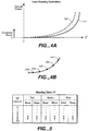
- FIG. 4A An example lens shading correction function 141 is illustrated in Figure 4A .
- the invention is generally applicable to the correction of a wide variety of shading non-uniformities from numerous causes. Shading non-uniformity can be attributed to non-uniform sensor sensitivity and internal camera reflections, to name just two. If variations caused by these sources were to be corrected for in combination with variations caused by lens characteristics, the actual correction function would be different, but the general approach would be the same.
- the correction is a relative zero.
- the center is preferably the point of an image of an object scene having uniform intensity thereacross where the detected image intensity is maximum.
- the intensity of the detected image then decreases as a function of radial distance r i away from that center.
- the amount of intensity correction applied to the detected image signal increases as a function of the radius r i 2 , as indicated by the curve 141.
- the amount that the image intensity is increased goes up rapidly at the edge of the image.
- This lens shading effect has been found to be circularly symmetrical; that is, the desired correction indicated by the curve 141 is substantially the same along any radial line extending across the detected image from its optical center.
- the curve 141 has been found in the general case to approximate an exponential function of the square of the radius; that is, the intensity correction for any image pixel is a function of a square of its radial distance from the optical center, f (r i 2 ).
- An equation can thus be written for each camera or other optical system that is solved by the DSP 55 or dedicated circuits for each pixel to determine the amount of correction for that pixel but it has been found to be more efficient to maintain a table of values of the curve 141 that are looked-up during the image processing.
- Figure 4B shows an expanded view of a portion of the curve 141, wherein the values of successive points 143-147 are taken to represent the curve.
- FIG. 5 An example of the shading table 77 ( Figure 2 ) is illustrated in Figure 5 .
- data of three separate correction curves are maintained, one for each of the primary colors red, green and blue.
- a second such curve 142 is shown in Figure 4A , for example.
- a base value of r i 2 is stored as well as a value of the slope of a straight line from that base value to the next base value.
- these circuits provide values of correction factors for the red, green and blue components of the detected image in time sequence, which are then used to correct the incoming video data as previously described with respect to Figure 3B .
- the table of Figure 5 needs to maintain only one set of base and slope numbers. In either case, the amount of data stored in the table 77 is small, so the size of the memory required to be included on the chip 43 to store it can be kept small.
- FIG. 6 An example technique implemented by circuits 73 ( Figure 2 ) for calculating r i 2 values to input to the calculation circuits 75 is illustrated in Figure 6 .
- the calculation is made from knowing the positions of the individual sensor photo-detectors in an x-y coordinate system, and then converting the measure of those positions to values of their radii from the optical center in a circular coordinate system.
- the calculation is simplified by using the fact that the photo-detectors are scanned in straight lines across the sensor 35, one row at a time, from one end to the other, in a raster pattern, until the outputs of all photo-detectors have been received to obtain a full frame of video data.
- a pixel 151 is the extreme upper-left pixel of the array, with a position designated as X 0 Y 0 since it is in the first row and first column of the array of pixels.
- the pixel 151 is the first pixel scanned when a frame of video data is being acquired.
- a pixel 153 is selected to be at the center of the shading pattern of the lens that images a scene onto the photo-detector array, and its location is noted as X C Y C .
- the address of the shading pattern center pixel 153 is designated as (0, 0). If this pixel is also the center pixel of the array, as is assumed for simplicity in this description, the pixel 151, in the small illustrative array being considered, carries an address of (10, 10).
- the next pixel to the right has an address of (9, 10), the first pixel of the second row (10, 9), and so forth.
- the radius of the first pixel 151 from the center X C Y C is designated as R 0 , and that of a generalized pixel x i y i as r i .
- the quantity r i 2 is calculated by the circuits 73 ( Figure 2 ) for each pixel from its rectangular coordinates (x i , y i ).
- the algorithm executed by the circuits 73 preferably relies upon arithmetic addition without the need for any of multiplication, division, square-root, or other more complicated arithmetic operations.
- the square of the radius of each pixel is calculated by the use of adders. This algorithm can now be described.
- R INIT 2
- Y 0 refers to the y-coordinate of the upper most line
- R 0 is the radius from the center (X C , Y C ) to the upper-left most pixel (X 0 , Y 0 ).
- the algorithm also accommodates scanning patterns that omit a proportion of the pixels or lines of pixels.
- the quantity H Y represents the number of lines in each step.
- the circuits 73 need only read that value from the registers 79 and apply it to the calculating circuits 75. But the radius function for the next pixel (9, 10), and the remaining pixels of a frame, need to be calculated by the circuits 73.
- R INIT 2 is the radius of the first pixel of the line calculated by equation (1) above
- X 0 refers to the x-coordinate of the initial pixel of the line
- H X is the number of pixels in each step
- a value of X 0 is stored in the non-volatile memory 49 during factory calibration and transferred to the registers 79 ( Figure 7 ) during system initialization, and H X 2 is stored by the DSP 55 for the type of scan that is to take place.
- the registers 79 also store at least one bit that is set by the DSP 55 to indicate when the shading correction is to be omitted.
- the R INIT 2 of each row after the first is calculated by adding the following to the the R INIT 2 of the immediately preceding line: 1 + 2 m Y H Y 2 where m y is the number of Hy steps passed from top row.
- the calculations of equations (3) and (4) are much simpler to make than those of equations (1) and (2), so the circuits 73 ( Figure 2 ) can be made simple and the radius function may be calculated for each new pixel.
- the simplified equation (3) is derived by taking differences of the radius function of equation (2) for successive pixels in a row.
- the simplified equation (4) is derived by taking differences of the radius function of equation (1) for successive lines of pixels.
- each unit is preferably calibrated as part of the manufacturing process and parameters resulting from that calibration stored in the non-volatile memory 49 ( Figure 2 ) for transfer during system initialization to the registers 79 ( Figures 2 and 7 ).
- a uniformly white two-dimensional scene 31 ( Figure 1 ) is imaged onto the sensor 35.
- the sensor 35 is then scanned and the image data stored directly in the memory 47 through the memory management unit 57, without lens shading correction or any other such modification. Because of the lens shading effect, however, the stored video data will not have a uniform intensity across the frame.
- This stored image frame data is then processed by the DSP 55 to determine the coordinates (X C , Y C ) of the center pixel 153 ( Figure 6 ) of the optical system, which is usually the point of maximum intensity of an image 29 ( Figure 1 ) of a scene 31 with a uniform intensity across it.
- the coordinates (X 0 , Y 0 ) of the upper-left corner pixel are determined by defining edges of the image frame on the photo-detector array of the sensor 35. After the center and corner coordinates have been determined, the maximum radius value R 0 2 is then calculated.
- This process corrects for any intensity shading introduced by the optical system 13, the sensor 29 ( Figure 1 ), or other internal camera variations, such as reflections off of internal camera surfaces. However, if the sensor 29 needs no correction, then the correction that is made is for the lens system 13 alone. Similarly, if the lens system 13 is made to form the image 29 without imparting intensity variations across it, then the correction that is made is for the sensor 29 alone.
Landscapes
- Engineering & Computer Science (AREA)
- Multimedia (AREA)
- Signal Processing (AREA)
- Studio Devices (AREA)
- Facsimile Image Signal Circuits (AREA)
- Transforming Light Signals Into Electric Signals (AREA)
- Color Television Image Signal Generators (AREA)
Claims (12)
- Verfahren zum Modifizieren eines digitalen Videosignals (37), das von einem Bildsensor (35) ausgegeben wird, der ein zweidimensionales Array aus einzelnen Pixeln mit einem darauf abgebildeten optischen Feld aufweist, wobei eine Sequenz von Ausgaben der einzelnen Pixel, die aus einer linearen Abtastung der Pixel über das optische Feld resultiert, das Videosignal bildet, aufweisend:Aufrechterhalten von Bildmodifikationsdaten in Abhängigkeit von den radialen Distanzen der Pixel von einer Mitte des auf den Bildsensor abgebildeten optischen Felds, wobei das Aufrechterhalten von Bildmodifikationsdaten das Speichern, in einem Speicher (47), von Intensitätskorrekturdatenpunkten auf einer kontinuierlichen Kurve entlang eines Radius über das abgebildete optische Feld von einer Mitte desselben und von Werten von Steigungen zwischen den Punkten aufweist,Berechnen der radialen Distanzen der einzelnen Pixel, die von ihrer linearen Position innerhalb des zweidimensionalen Arrays abgetastet werden,Generieren von Bildmodifikationen für die einzelnen abgetasteten Pixel durch das Nachschlagen der Bildmodifikationsdaten in dem Speicher (47) in Entsprechung zu den berechneten radialen Distanzen derselben, wobei für radiale Distanzen zwischen zwei gespeicherten Datenpunkten die Bildmodifikationsdaten unter Verwendung der gespeicherten Steigung zwischen diesen Datenpunkten interpoliert werden, undKombinieren der generierten Bildmodifikationsdaten mit den Ausgaben von entsprechenden einzelnen abgetasteten Pixeln, um dadurch die Sequenz von Ausgaben der einzelnen Pixel in Entsprechung zu den Bildmodifikationsdaten zu modifizieren.
- Verfahren nach Anspruch 1, wobei die Schritte zum Berechnen, Generieren und Kombinieren für die einzelnen abgetasteten Pixel wenigstens so schnell durchgeführt werden, wie die Sequenz von Ausgaben der abgetasteten Pixel in dem von dem Bildsensor (35) ausgegebenen Videosignal (37) erscheinen.
- Verfahren nach Anspruch 1, wobei die aufrechterhaltenen Bildmodifikationsdaten eine Korrektur der einzelnen Pixel für Intensitätsvariationen über das optische Feld enthalten, die durch ein das optische Feld an dem Bildsensor (35) abbildendes optisches System (13), durch den Bildsensor selbst oder durch Lichtreflexionen von internen Flächen einer das optische System und den Bildsensor (35) enthaltenden Umhausung eingeführt werden.
- Verfahren nach Anspruch 1, wobei das Aufrechterhalten der Bildmodifikationsdaten das Aufrechterhalten einer Vielzahl von Sätzen von Bildmodifikationsdaten für die einzelnen abgetasteten Pixel aufweist, wobei jeweils ein Satz von Daten für jeden aus einer Vielzahl von Farbkomponenten des optischen Felds vorgesehen ist.
- Verfahren nach Anspruch 1, wobei die Funktionen zum Aufrechterhalten, Berechnen und Generieren alle auf einem einzelnen IC-Chip (43) durchgeführt werden.
- Verfahren nach Anspruch 1, wobei die Funktionen zum Aufrechterhalten, Berechnen und Generieren durch elektronische Schaltkreise, die eigens für das Durchführen dieser Funktionen vorgesehen sind, durchgeführt werden.
- Verfahren nach Anspruch 1, wobei die kontinuierliche Kurve, auf der die Intensitätskorrekturdatenpunkte liegen, durch eine Exponentialfunktion des Radius definiert werden.
- Verfahren nach Anspruch 1, wobei die Werte der gespeicherten Punkte über den Bildsensor (35) durch ein optisches System (13) für das Betrachten eines Bildfelds mit einer gleichmäßigen Intensität und einer Entsprechung zu der kontinuierlichen Kurve gemessen werden.
- Eine Videoaufnahmevorrichtung, aufweisend:einen optischen Sensor (35), der ein zweidimensionales Array von Detektoren aufweist, die in einem Rastermuster abgetastet werden, um einen seriellen Strom von Daten auszugeben, die eine Intensität einer optischen Strahlung auf diesem wiedergeben,ein optisches System (13), das in Bezug auf den Sensor (35) fixiert ist, um ein optisches Strahlungsfeld auf den Sensor (35) abzubilden,einen Speicher (47), der Sphärische-Intensität-Korrekturdaten für den optischen Sensor (35) und das optische System (13) speichert, wobei die Korrekturdaten als Datenpunkte auf einer kontinuierlichen Kurve (141), die sich entlang eines Radius über das abgebildete optische Feld von einer Mitte desselben erstreckt, und als Werte von Steigungen zwischen diesen Datenpunkten gespeichert werden,dedizierte Berechnungsschaltungen (73), die Positionen des Rasterabtastungsmusters zu Radialdistanzen über das optische Feld wandeln,dedizierte Korrekturbestimmungsschaltungen (75), die Werte aus dem Speicher (47) für die berechneten radialen Distanzen lesen und aus diesen eine Größe der auf dem seriellen Strom von Daten vorzunehmenden Intensitätskorrektur berechnen, wobei für radiale Distanzen zwischen zwei gespeicherten Datenpunkten die Bildmodifikationsdaten unter Verwendung der gespeicherten Steigung zwischen diesen Datenpunkten interpoliert werden, undKombinationsschaltungen (63), die den aus dem optischen Sensor (35) ausgegebenen seriellen Strom von Daten mit der berechneten Größe der Intensitätskorrektur modifizieren, um dadurch den seriellen Strom von Daten für Intensitätsvariationen über das abgebildete optische Feld zu korrigieren.
- Bildaufnahmevorrichtung nach Anspruch 9, wobei Werte der gespeicherten Punkte über den optischen Sensor (35) durch das optische System zum Betrachten eines Bildfelds mit einer gleichförmigen Intensität gemessen wurden.
- Bildaufnahmevorrichtung nach Anspruch 9 oder 10, wobei die kontinuierliche Kurve (141), auf der die Sphärische-Intensität-Korrekturdatenpunkte liegen, durch eine Exponentialfunktion des Radius definiert wird.
- Bildaufnahmevorrichtung nach Anspruch 9 oder 10, wobei der Sensor (35) einen seriellen Strom von Daten ausgibt, die die Intensität einer Vielzahl von einzelnen Farbkomponenten der auf den Sensor (35) einfallenden optischen Strahlung wiedergeben, und der Speicher (47) Korrekturdaten für jede aus der Vielzahl von Farbkomponenten speichert.
Applications Claiming Priority (3)
| Application Number | Priority Date | Filing Date | Title |
|---|---|---|---|
| US222412 | 1988-07-21 | ||
| US10/222,412 US7408576B2 (en) | 2002-08-16 | 2002-08-16 | Techniques for modifying image field data as a function of radius across the image field |
| PCT/US2003/024189 WO2004017627A1 (en) | 2002-08-16 | 2003-08-01 | Shading correction method for image reading means |
Publications (2)
| Publication Number | Publication Date |
|---|---|
| EP1529395A1 EP1529395A1 (de) | 2005-05-11 |
| EP1529395B1 true EP1529395B1 (de) | 2018-05-02 |
Family
ID=31714954
Family Applications (1)
| Application Number | Title | Priority Date | Filing Date |
|---|---|---|---|
| EP03788314.7A Expired - Lifetime EP1529395B1 (de) | 2002-08-16 | 2003-08-01 | Schattierungskorrekturverfahren für eine bildlesevorrichtung |
Country Status (5)
| Country | Link |
|---|---|
| US (2) | US7408576B2 (de) |
| EP (1) | EP1529395B1 (de) |
| JP (1) | JP4309345B2 (de) |
| AU (1) | AU2003258009A1 (de) |
| WO (1) | WO2004017627A1 (de) |
Families Citing this family (38)
| Publication number | Priority date | Publication date | Assignee | Title |
|---|---|---|---|---|
| US7388610B2 (en) | 2002-08-16 | 2008-06-17 | Zoran Corporation | Techniques of modifying image field data by extrapolation |
| US7408576B2 (en) * | 2002-08-16 | 2008-08-05 | Zoran Corporation | Techniques for modifying image field data as a function of radius across the image field |
| US7391450B2 (en) * | 2002-08-16 | 2008-06-24 | Zoran Corporation | Techniques for modifying image field data |
| JP2004165958A (ja) * | 2002-11-13 | 2004-06-10 | Renesas Technology Corp | カメラモジュール |
| WO2005043891A1 (ja) * | 2003-10-31 | 2005-05-12 | Mitsubishi Denki Kabushiki Kaisha | 画像補正方法および撮像装置 |
| US7609305B2 (en) * | 2004-04-06 | 2009-10-27 | Samsung Electronics Co., Ltd. | Methods and systems for anti shading correction in image sensors |
| WO2005122549A1 (en) | 2004-06-07 | 2005-12-22 | Nokia Corporation | Method, apparatus, imaging module and program for improving image quality in a digital imaging device |
| TWI375112B (en) * | 2004-06-24 | 2012-10-21 | Pentax Ricoh Imaging Co Ltd | Digital camera |
| KR100615277B1 (ko) * | 2004-08-18 | 2006-08-25 | 엠텍비젼 주식회사 | 이미지 센서에서의 렌즈 셰이딩 현상 보정 방법 및 장치 |
| US7961973B2 (en) | 2004-09-02 | 2011-06-14 | Qualcomm Incorporated | Lens roll-off correction method and apparatus |
| US7215493B2 (en) * | 2005-01-27 | 2007-05-08 | Psc Scanning, Inc. | Imaging system with a lens having increased light collection efficiency and a deblurring equalizer |
| US8259179B2 (en) * | 2006-05-15 | 2012-09-04 | Csr Technology Inc. | Compensating for non-uniform illumination of object fields captured by a camera |
| KR100696162B1 (ko) * | 2006-08-11 | 2007-03-20 | 엠텍비젼 주식회사 | 이미지의 노이즈 감소 장치 및 노이즈 감소 방법, 이를수행하는 프로그램이 기록된 기록 매체 |
| GB2442050A (en) * | 2006-08-29 | 2008-03-26 | Micron Technology Inc | Image pixel value correction |
| US7782380B2 (en) * | 2006-09-01 | 2010-08-24 | Aptina Imaging Corporation | Positional gain adjustment and surface generation for image processing |
| JP2008160730A (ja) * | 2006-12-26 | 2008-07-10 | Nikon Corp | 信号ムラを修正する画像処理装置、較正方法、撮像装置、画像処理プログラム、および画像処理方法 |
| JP4653123B2 (ja) * | 2007-01-09 | 2011-03-16 | 富士フイルム株式会社 | 画像取得装置および画像取得方法 |
| US7755671B2 (en) * | 2007-04-23 | 2010-07-13 | Hewlett-Packard Development Company, L.P. | Correcting a captured image in digital imaging devices |
| US20080278613A1 (en) * | 2007-05-11 | 2008-11-13 | Micron Technology, Inc. | Methods, apparatuses and systems providing pixel value adjustment for images produced with varying focal length lenses |
| US8078001B2 (en) | 2007-05-11 | 2011-12-13 | Micron Technology, Inc. | Methods, apparatuses and systems for piecewise generation of pixel correction values for image processing |
| US7920171B2 (en) * | 2007-05-18 | 2011-04-05 | Aptina Imaging Corporation | Methods and apparatuses for vignetting correction in image signals |
| US8463068B2 (en) * | 2007-08-09 | 2013-06-11 | Micron Technology, Inc. | Methods, systems and apparatuses for pixel value correction using multiple vertical and/or horizontal correction curves |
| US8331722B2 (en) * | 2008-01-08 | 2012-12-11 | Aptina Imaging Corporation | Methods, apparatuses and systems providing pixel value adjustment for images produced by a camera having multiple optical states |
| GB0801443D0 (en) * | 2008-01-25 | 2008-03-05 | Micron Technology Inc | Methods, systems and apparatuses for pixel signal correction using elliptical hyperbolic cosines |
| KR101672944B1 (ko) * | 2009-12-14 | 2016-11-04 | 엘지이노텍 주식회사 | 오토 포커스 카메라 모듈에서의 렌즈 셰이딩 보상방법 |
| US8542919B2 (en) | 2010-06-22 | 2013-09-24 | SK Hynix Inc. | Method and system for correcting lens shading |
| TWI458347B (zh) | 2010-12-20 | 2014-10-21 | 財團法人工業技術研究院 | 影像擷取裝置及其方法 |
| JP5454622B2 (ja) * | 2012-06-06 | 2014-03-26 | カシオ計算機株式会社 | 撮像装置、合成画像生成方法、及び、プログラム |
| WO2015038810A2 (en) | 2013-09-11 | 2015-03-19 | Firima Inc. | User interface based on optical sensing and tracking of user's eye movement and position |
| WO2015070182A2 (en) * | 2013-11-09 | 2015-05-14 | Firima Inc. | Optical eye tracking |
| WO2015081325A1 (en) | 2013-11-27 | 2015-06-04 | Shenzhen Huiding Technology Co., Ltd. | Eye tracking and user reaction detection |
| CN105488869A (zh) * | 2014-09-16 | 2016-04-13 | 深圳富泰宏精密工业有限公司 | 密码锁开锁系统及方法 |
| US10368067B2 (en) | 2016-06-15 | 2019-07-30 | Mediatek Inc. | Method and apparatus for selective filtering of cubic-face frames |
| US10148939B2 (en) | 2016-07-19 | 2018-12-04 | Gopro, Inc. | Mapping of spherical image data into rectangular faces for transport and decoding across networks |
| US10356346B1 (en) * | 2018-02-26 | 2019-07-16 | Fotonation Limited | Method for compensating for off-axis tilting of a lens |
| DE102018115991B4 (de) | 2018-07-02 | 2023-12-07 | Basler Ag | Digitale schaltung zur korrektur eines vignettierungseffekts in werten von pixeln eines bildes einer elektronischen kamera |
| KR20220142135A (ko) | 2021-04-14 | 2022-10-21 | 삼성전자주식회사 | 반사체 및 렌즈 어셈블리를 포함하는 전자 장치 |
| KR20240119609A (ko) * | 2023-01-30 | 2024-08-06 | 삼성전자주식회사 | 렌즈 쉐이딩 정정 회로 및 렌즈 쉐이딩 정정 방법을 포함하는 이미지 처리 시스템 |
Citations (1)
| Publication number | Priority date | Publication date | Assignee | Title |
|---|---|---|---|---|
| US3743772A (en) * | 1969-11-12 | 1973-07-03 | Meldreth Electronics Ltd | Image analysing |
Family Cites Families (34)
| Publication number | Priority date | Publication date | Assignee | Title |
|---|---|---|---|---|
| US4482975A (en) | 1982-03-29 | 1984-11-13 | Motorola, Inc. | Function generator |
| JPS60182870A (ja) | 1984-03-01 | 1985-09-18 | Canon Inc | 画像処理装置 |
| US5267055A (en) | 1988-05-11 | 1993-11-30 | Canon Kabushiki Kaisha | Image signal processing apparatus |
| FR2657208B1 (fr) | 1990-01-16 | 1992-04-10 | Thomson Consumer Electronics | Procede et dispositif de correction automatique de geometrie, de superposition de couleurs et d'uniformite d'image pour camera de television. |
| US5047861A (en) | 1990-07-31 | 1991-09-10 | Eastman Kodak Company | Method and apparatus for pixel non-uniformity correction |
| JP2893078B2 (ja) * | 1990-12-06 | 1999-05-17 | オムロン株式会社 | シェーディング補正方法およびその装置 |
| JP3191354B2 (ja) | 1991-11-15 | 2001-07-23 | ソニー株式会社 | シェーディング補正回路 |
| JPH0865546A (ja) | 1994-08-18 | 1996-03-08 | Fuji Photo Film Co Ltd | シェーディング補正係数生成回路およびシェーディング補正係数生成方法 |
| DE69526635T2 (de) | 1994-12-29 | 2002-12-05 | Koninklijke Philips Electronics N.V., Eindhoven | Bilderzeugungsgerät und Verfahren zur Verbesserung geometrischer optischer Bildverzerrungen |
| DE69707223T2 (de) * | 1996-03-18 | 2002-06-13 | Koninklijke Philips Electronics N.V., Eindhoven | Streulichtkompensation |
| JPH09307789A (ja) | 1996-05-17 | 1997-11-28 | Olympus Optical Co Ltd | 画像処理装置 |
| JP3675066B2 (ja) | 1996-11-06 | 2005-07-27 | 三菱電機株式会社 | 赤外線撮像装置および画像補正方法 |
| JPH10160566A (ja) | 1996-12-03 | 1998-06-19 | Mitsubishi Electric Corp | 赤外線撮像装置 |
| JP3822723B2 (ja) | 1997-08-29 | 2006-09-20 | 富士写真フイルム株式会社 | 画像処理装置 |
| DE19855885A1 (de) | 1997-12-04 | 1999-08-05 | Fuji Photo Film Co Ltd | Bildverarbeitungsverfahren und -vorrichtung |
| JP4327928B2 (ja) * | 1999-02-26 | 2009-09-09 | メディア・テック・ユーエスエイ・インコーポレーテッド | 電子カメラ装置 |
| US6727521B2 (en) | 2000-09-25 | 2004-04-27 | Foveon, Inc. | Vertical color filter detector group and array |
| US6833862B1 (en) * | 1999-06-30 | 2004-12-21 | Logitech, Inc. | Image sensor based vignetting correction |
| JP2001274973A (ja) | 2000-03-24 | 2001-10-05 | Sanyo Electric Co Ltd | 顕微鏡画像合成装置、顕微鏡画像合成方法、顕微鏡画像合成処理プログラムを記録したコンピュータ読み取り可能な記録媒体 |
| JP2002125156A (ja) * | 2000-08-11 | 2002-04-26 | Nikon Corp | 固体撮像素子及び電子カメラ |
| JP4574022B2 (ja) * | 2001-01-17 | 2010-11-04 | キヤノン株式会社 | 撮像装置及びシェーディング補正方法 |
| JP2002216136A (ja) | 2001-01-23 | 2002-08-02 | Sony Corp | 距離算出方法及び撮像装置 |
| US6853402B2 (en) * | 2001-01-30 | 2005-02-08 | Xerox Corporation | Combined multiplexing and offset correction for an image sensor array |
| JP2002237998A (ja) | 2001-02-07 | 2002-08-23 | Sony Corp | 画面補正方法及び撮像装置 |
| JP3539394B2 (ja) | 2001-03-26 | 2004-07-07 | ミノルタ株式会社 | 画像処理装置、プログラムおよび記録媒体 |
| US6983298B2 (en) | 2001-03-28 | 2006-01-03 | Texas Instruments Incorporated | Method and apparatus for linear interpolation using gradient tables |
| US6940546B2 (en) | 2001-04-04 | 2005-09-06 | Eastman Kodak Company | Method for compensating a digital image for light falloff while minimizing light balance change |
| US6975775B2 (en) * | 2002-03-06 | 2005-12-13 | Radiant Imaging, Inc. | Stray light correction method for imaging light and color measurement system |
| JP2004038728A (ja) | 2002-07-05 | 2004-02-05 | Noritsu Koki Co Ltd | 画像処理方法、画像処理プログラム、および、画像処理プログラムを記録した記録媒体 |
| US7391450B2 (en) | 2002-08-16 | 2008-06-24 | Zoran Corporation | Techniques for modifying image field data |
| US7388610B2 (en) | 2002-08-16 | 2008-06-17 | Zoran Corporation | Techniques of modifying image field data by extrapolation |
| US7408576B2 (en) * | 2002-08-16 | 2008-08-05 | Zoran Corporation | Techniques for modifying image field data as a function of radius across the image field |
| US20050025164A1 (en) * | 2003-07-16 | 2005-02-03 | Telefonaktiebolaget L M Ericsson (Publ) | Seamless hand-off of mobile node to a wireless local area network (WLAN) |
| WO2005043891A1 (ja) | 2003-10-31 | 2005-05-12 | Mitsubishi Denki Kabushiki Kaisha | 画像補正方法および撮像装置 |
-
2002
- 2002-08-16 US US10/222,412 patent/US7408576B2/en not_active Expired - Lifetime
-
2003
- 2003-08-01 EP EP03788314.7A patent/EP1529395B1/de not_active Expired - Lifetime
- 2003-08-01 JP JP2004529235A patent/JP4309345B2/ja not_active Expired - Fee Related
- 2003-08-01 WO PCT/US2003/024189 patent/WO2004017627A1/en not_active Ceased
- 2003-08-01 AU AU2003258009A patent/AU2003258009A1/en not_active Abandoned
-
2008
- 2008-07-18 US US12/176,283 patent/US7907195B2/en not_active Expired - Lifetime
Patent Citations (1)
| Publication number | Priority date | Publication date | Assignee | Title |
|---|---|---|---|---|
| US3743772A (en) * | 1969-11-12 | 1973-07-03 | Meldreth Electronics Ltd | Image analysing |
Also Published As
| Publication number | Publication date |
|---|---|
| US7907195B2 (en) | 2011-03-15 |
| US7408576B2 (en) | 2008-08-05 |
| AU2003258009A1 (en) | 2004-03-03 |
| JP2005536148A (ja) | 2005-11-24 |
| JP4309345B2 (ja) | 2009-08-05 |
| WO2004017627A1 (en) | 2004-02-26 |
| US20080273103A1 (en) | 2008-11-06 |
| US20040032952A1 (en) | 2004-02-19 |
| EP1529395A1 (de) | 2005-05-11 |
Similar Documents
| Publication | Publication Date | Title |
|---|---|---|
| EP1529395B1 (de) | Schattierungskorrekturverfahren für eine bildlesevorrichtung | |
| EP1700268B1 (de) | Techniken zum modifizieren von bildfelddaten | |
| EP1711880B1 (de) | Techniken zum modifizieren von bildfelddaten durch extrapolation | |
| JP4161295B2 (ja) | 画像センサのダイナミックレンジを拡大するカラー画像撮像システム | |
| US8934035B2 (en) | Correction of non-uniform sensitivity in an image array | |
| CN101816171B (zh) | 用于增强图像动态范围的多重曝光模式 | |
| US6873442B1 (en) | Method and system for generating a low resolution image from a sparsely sampled extended dynamic range image sensing device | |
| WO2007133898A1 (en) | Compensating for non-uniform illumination of object fields captured by a camera | |
| US20110150357A1 (en) | Method for creating high dynamic range image | |
| US20100231765A1 (en) | Method and arrangement for generating a color video signal | |
| US7755672B2 (en) | Techniques for modifying image field data obtained using illumination sources | |
| EP1067777B1 (de) | Bildaufnahmegerät, Gerät und Verfahren zur Bildverarbeitung, und Speichermedium | |
| CN113747066A (zh) | 图像校正方法、装置、电子设备及计算机可读存储介质 | |
| JP2002525722A (ja) | 画像処理方法とシステム | |
| US20090190006A1 (en) | Methods, systems and apparatuses for pixel signal correction using elliptical hyperbolic cosines |
Legal Events
| Date | Code | Title | Description |
|---|---|---|---|
| PUAI | Public reference made under article 153(3) epc to a published international application that has entered the european phase |
Free format text: ORIGINAL CODE: 0009012 |
|
| 17P | Request for examination filed |
Effective date: 20050214 |
|
| AK | Designated contracting states |
Kind code of ref document: A1 Designated state(s): AT BE BG CH CY CZ DE DK EE ES FI FR GB GR HU IE IT LI LU MC NL PT RO SE SI SK TR |
|
| AX | Request for extension of the european patent |
Extension state: AL LT LV MK |
|
| DAX | Request for extension of the european patent (deleted) | ||
| RIN1 | Information on inventor provided before grant (corrected) |
Inventor name: GALIL, EREZ Inventor name: PINTO, VICTOR |
|
| 17Q | First examination report despatched |
Effective date: 20131014 |
|
| RAP1 | Party data changed (applicant data changed or rights of an application transferred) |
Owner name: QUALCOMM TECHNOLOGIES, INC. |
|
| STAA | Information on the status of an ep patent application or granted ep patent |
Free format text: STATUS: EXAMINATION IS IN PROGRESS |
|
| GRAP | Despatch of communication of intention to grant a patent |
Free format text: ORIGINAL CODE: EPIDOSNIGR1 |
|
| STAA | Information on the status of an ep patent application or granted ep patent |
Free format text: STATUS: GRANT OF PATENT IS INTENDED |
|
| RAP1 | Party data changed (applicant data changed or rights of an application transferred) |
Owner name: QUALCOMM INCORPORATED |
|
| INTG | Intention to grant announced |
Effective date: 20171122 |
|
| GRAS | Grant fee paid |
Free format text: ORIGINAL CODE: EPIDOSNIGR3 |
|
| GRAA | (expected) grant |
Free format text: ORIGINAL CODE: 0009210 |
|
| STAA | Information on the status of an ep patent application or granted ep patent |
Free format text: STATUS: THE PATENT HAS BEEN GRANTED |
|
| AK | Designated contracting states |
Kind code of ref document: B1 Designated state(s): AT BE BG CH CY CZ DE DK EE ES FI FR GB GR HU IE IT LI LU MC NL PT RO SE SI SK TR |
|
| REG | Reference to a national code |
Ref country code: GB Ref legal event code: FG4D |
|
| REG | Reference to a national code |
Ref country code: CH Ref legal event code: EP Ref country code: AT Ref legal event code: REF Ref document number: 996451 Country of ref document: AT Kind code of ref document: T Effective date: 20180515 |
|
| REG | Reference to a national code |
Ref country code: DE Ref legal event code: R096 Ref document number: 60351170 Country of ref document: DE |
|
| REG | Reference to a national code |
Ref country code: IE Ref legal event code: FG4D |
|
| REG | Reference to a national code |
Ref country code: FR Ref legal event code: PLFP Year of fee payment: 16 |
|
| REG | Reference to a national code |
Ref country code: NL Ref legal event code: MP Effective date: 20180502 |
|
| PG25 | Lapsed in a contracting state [announced via postgrant information from national office to epo] |
Ref country code: ES Free format text: LAPSE BECAUSE OF FAILURE TO SUBMIT A TRANSLATION OF THE DESCRIPTION OR TO PAY THE FEE WITHIN THE PRESCRIBED TIME-LIMIT Effective date: 20180502 Ref country code: SE Free format text: LAPSE BECAUSE OF FAILURE TO SUBMIT A TRANSLATION OF THE DESCRIPTION OR TO PAY THE FEE WITHIN THE PRESCRIBED TIME-LIMIT Effective date: 20180502 Ref country code: BG Free format text: LAPSE BECAUSE OF FAILURE TO SUBMIT A TRANSLATION OF THE DESCRIPTION OR TO PAY THE FEE WITHIN THE PRESCRIBED TIME-LIMIT Effective date: 20180802 Ref country code: FI Free format text: LAPSE BECAUSE OF FAILURE TO SUBMIT A TRANSLATION OF THE DESCRIPTION OR TO PAY THE FEE WITHIN THE PRESCRIBED TIME-LIMIT Effective date: 20180502 |
|
| PG25 | Lapsed in a contracting state [announced via postgrant information from national office to epo] |
Ref country code: GR Free format text: LAPSE BECAUSE OF FAILURE TO SUBMIT A TRANSLATION OF THE DESCRIPTION OR TO PAY THE FEE WITHIN THE PRESCRIBED TIME-LIMIT Effective date: 20180803 Ref country code: NL Free format text: LAPSE BECAUSE OF FAILURE TO SUBMIT A TRANSLATION OF THE DESCRIPTION OR TO PAY THE FEE WITHIN THE PRESCRIBED TIME-LIMIT Effective date: 20180502 |
|
| REG | Reference to a national code |
Ref country code: AT Ref legal event code: MK05 Ref document number: 996451 Country of ref document: AT Kind code of ref document: T Effective date: 20180502 |
|
| PG25 | Lapsed in a contracting state [announced via postgrant information from national office to epo] |
Ref country code: PT Free format text: LAPSE BECAUSE OF FAILURE TO SUBMIT A TRANSLATION OF THE DESCRIPTION OR TO PAY THE FEE WITHIN THE PRESCRIBED TIME-LIMIT Effective date: 20180903 |
|
| PG25 | Lapsed in a contracting state [announced via postgrant information from national office to epo] |
Ref country code: CZ Free format text: LAPSE BECAUSE OF FAILURE TO SUBMIT A TRANSLATION OF THE DESCRIPTION OR TO PAY THE FEE WITHIN THE PRESCRIBED TIME-LIMIT Effective date: 20180502 Ref country code: RO Free format text: LAPSE BECAUSE OF FAILURE TO SUBMIT A TRANSLATION OF THE DESCRIPTION OR TO PAY THE FEE WITHIN THE PRESCRIBED TIME-LIMIT Effective date: 20180502 Ref country code: SK Free format text: LAPSE BECAUSE OF FAILURE TO SUBMIT A TRANSLATION OF THE DESCRIPTION OR TO PAY THE FEE WITHIN THE PRESCRIBED TIME-LIMIT Effective date: 20180502 Ref country code: DK Free format text: LAPSE BECAUSE OF FAILURE TO SUBMIT A TRANSLATION OF THE DESCRIPTION OR TO PAY THE FEE WITHIN THE PRESCRIBED TIME-LIMIT Effective date: 20180502 Ref country code: EE Free format text: LAPSE BECAUSE OF FAILURE TO SUBMIT A TRANSLATION OF THE DESCRIPTION OR TO PAY THE FEE WITHIN THE PRESCRIBED TIME-LIMIT Effective date: 20180502 Ref country code: AT Free format text: LAPSE BECAUSE OF FAILURE TO SUBMIT A TRANSLATION OF THE DESCRIPTION OR TO PAY THE FEE WITHIN THE PRESCRIBED TIME-LIMIT Effective date: 20180502 |
|
| REG | Reference to a national code |
Ref country code: DE Ref legal event code: R097 Ref document number: 60351170 Country of ref document: DE |
|
| PG25 | Lapsed in a contracting state [announced via postgrant information from national office to epo] |
Ref country code: IT Free format text: LAPSE BECAUSE OF FAILURE TO SUBMIT A TRANSLATION OF THE DESCRIPTION OR TO PAY THE FEE WITHIN THE PRESCRIBED TIME-LIMIT Effective date: 20180502 |
|
| PLBE | No opposition filed within time limit |
Free format text: ORIGINAL CODE: 0009261 |
|
| STAA | Information on the status of an ep patent application or granted ep patent |
Free format text: STATUS: NO OPPOSITION FILED WITHIN TIME LIMIT |
|
| PG25 | Lapsed in a contracting state [announced via postgrant information from national office to epo] |
Ref country code: MC Free format text: LAPSE BECAUSE OF FAILURE TO SUBMIT A TRANSLATION OF THE DESCRIPTION OR TO PAY THE FEE WITHIN THE PRESCRIBED TIME-LIMIT Effective date: 20180502 |
|
| REG | Reference to a national code |
Ref country code: CH Ref legal event code: PL |
|
| 26N | No opposition filed |
Effective date: 20190205 |
|
| PG25 | Lapsed in a contracting state [announced via postgrant information from national office to epo] |
Ref country code: LU Free format text: LAPSE BECAUSE OF NON-PAYMENT OF DUE FEES Effective date: 20180801 Ref country code: CH Free format text: LAPSE BECAUSE OF NON-PAYMENT OF DUE FEES Effective date: 20180831 Ref country code: LI Free format text: LAPSE BECAUSE OF NON-PAYMENT OF DUE FEES Effective date: 20180831 |
|
| REG | Reference to a national code |
Ref country code: BE Ref legal event code: MM Effective date: 20180831 |
|
| REG | Reference to a national code |
Ref country code: IE Ref legal event code: MM4A |
|
| PG25 | Lapsed in a contracting state [announced via postgrant information from national office to epo] |
Ref country code: SI Free format text: LAPSE BECAUSE OF FAILURE TO SUBMIT A TRANSLATION OF THE DESCRIPTION OR TO PAY THE FEE WITHIN THE PRESCRIBED TIME-LIMIT Effective date: 20180502 |
|
| PG25 | Lapsed in a contracting state [announced via postgrant information from national office to epo] |
Ref country code: IE Free format text: LAPSE BECAUSE OF NON-PAYMENT OF DUE FEES Effective date: 20180801 |
|
| PG25 | Lapsed in a contracting state [announced via postgrant information from national office to epo] |
Ref country code: BE Free format text: LAPSE BECAUSE OF NON-PAYMENT OF DUE FEES Effective date: 20180831 |
|
| PG25 | Lapsed in a contracting state [announced via postgrant information from national office to epo] |
Ref country code: TR Free format text: LAPSE BECAUSE OF FAILURE TO SUBMIT A TRANSLATION OF THE DESCRIPTION OR TO PAY THE FEE WITHIN THE PRESCRIBED TIME-LIMIT Effective date: 20180502 |
|
| PG25 | Lapsed in a contracting state [announced via postgrant information from national office to epo] |
Ref country code: HU Free format text: LAPSE BECAUSE OF FAILURE TO SUBMIT A TRANSLATION OF THE DESCRIPTION OR TO PAY THE FEE WITHIN THE PRESCRIBED TIME-LIMIT; INVALID AB INITIO Effective date: 20030801 |
|
| PG25 | Lapsed in a contracting state [announced via postgrant information from national office to epo] |
Ref country code: CY Free format text: LAPSE BECAUSE OF FAILURE TO SUBMIT A TRANSLATION OF THE DESCRIPTION OR TO PAY THE FEE WITHIN THE PRESCRIBED TIME-LIMIT Effective date: 20180502 |
|
| PGFP | Annual fee paid to national office [announced via postgrant information from national office to epo] |
Ref country code: GB Payment date: 20220726 Year of fee payment: 20 Ref country code: DE Payment date: 20220615 Year of fee payment: 20 |
|
| REG | Reference to a national code |
Ref country code: DE Ref legal event code: R079 Ref document number: 60351170 Country of ref document: DE Free format text: PREVIOUS MAIN CLASS: H04N0005217000 Ipc: H04N0023800000 |
|
| PGFP | Annual fee paid to national office [announced via postgrant information from national office to epo] |
Ref country code: FR Payment date: 20220713 Year of fee payment: 20 |
|
| REG | Reference to a national code |
Ref country code: DE Ref legal event code: R071 Ref document number: 60351170 Country of ref document: DE |
|
| REG | Reference to a national code |
Ref country code: GB Ref legal event code: PE20 Expiry date: 20230731 |
|
| PG25 | Lapsed in a contracting state [announced via postgrant information from national office to epo] |
Ref country code: GB Free format text: LAPSE BECAUSE OF EXPIRATION OF PROTECTION Effective date: 20230731 |