EP1528846B1 - Source EUV - Google Patents
Source EUV Download PDFInfo
- Publication number
- EP1528846B1 EP1528846B1 EP04292256A EP04292256A EP1528846B1 EP 1528846 B1 EP1528846 B1 EP 1528846B1 EP 04292256 A EP04292256 A EP 04292256A EP 04292256 A EP04292256 A EP 04292256A EP 1528846 B1 EP1528846 B1 EP 1528846B1
- Authority
- EP
- European Patent Office
- Prior art keywords
- radiation
- pressure
- irradiation
- chamber
- euv
- Prior art date
- Legal status (The legal status is an assumption and is not a legal conclusion. Google has not performed a legal analysis and makes no representation as to the accuracy of the status listed.)
- Expired - Lifetime
Links
- 230000005855 radiation Effects 0.000 claims abstract description 122
- 230000005540 biological transmission Effects 0.000 claims abstract description 44
- 239000000463 material Substances 0.000 claims abstract description 32
- 230000003287 optical effect Effects 0.000 claims abstract description 23
- 238000000206 photolithography Methods 0.000 claims abstract description 19
- 230000003750 conditioning effect Effects 0.000 claims abstract description 6
- 239000004065 semiconductor Substances 0.000 claims description 23
- 238000000034 method Methods 0.000 claims description 13
- 229910052724 xenon Inorganic materials 0.000 claims description 12
- FHNFHKCVQCLJFQ-UHFFFAOYSA-N xenon atom Chemical compound [Xe] FHNFHKCVQCLJFQ-UHFFFAOYSA-N 0.000 claims description 12
- XKRFYHLGVUSROY-UHFFFAOYSA-N Argon Chemical compound [Ar] XKRFYHLGVUSROY-UHFFFAOYSA-N 0.000 claims description 10
- 239000007788 liquid Substances 0.000 claims description 6
- 229910052786 argon Inorganic materials 0.000 claims description 5
- 229910052734 helium Inorganic materials 0.000 claims description 5
- 239000001307 helium Substances 0.000 claims description 5
- SWQJXJOGLNCZEY-UHFFFAOYSA-N helium atom Chemical compound [He] SWQJXJOGLNCZEY-UHFFFAOYSA-N 0.000 claims description 5
- 239000002245 particle Substances 0.000 claims description 5
- ATJFFYVFTNAWJD-UHFFFAOYSA-N Tin Chemical compound [Sn] ATJFFYVFTNAWJD-UHFFFAOYSA-N 0.000 claims description 4
- 229910052743 krypton Inorganic materials 0.000 claims description 4
- DNNSSWSSYDEUBZ-UHFFFAOYSA-N krypton atom Chemical compound [Kr] DNNSSWSSYDEUBZ-UHFFFAOYSA-N 0.000 claims description 4
- 150000002500 ions Chemical class 0.000 claims description 3
- 235000012431 wafers Nutrition 0.000 description 13
- 239000007789 gas Substances 0.000 description 11
- 230000004907 flux Effects 0.000 description 7
- 239000010410 layer Substances 0.000 description 7
- 238000004519 manufacturing process Methods 0.000 description 7
- 238000004377 microelectronic Methods 0.000 description 5
- 238000005086 pumping Methods 0.000 description 5
- 238000010521 absorption reaction Methods 0.000 description 3
- 239000003638 chemical reducing agent Substances 0.000 description 3
- 239000000203 mixture Substances 0.000 description 3
- 238000004064 recycling Methods 0.000 description 3
- 229910001128 Sn alloy Inorganic materials 0.000 description 2
- 238000009434 installation Methods 0.000 description 2
- 239000007787 solid Substances 0.000 description 2
- 238000011144 upstream manufacturing Methods 0.000 description 2
- 229910000846 In alloy Inorganic materials 0.000 description 1
- 229910000978 Pb alloy Inorganic materials 0.000 description 1
- 229920000297 Rayon Polymers 0.000 description 1
- 230000015572 biosynthetic process Effects 0.000 description 1
- 238000006243 chemical reaction Methods 0.000 description 1
- 238000010586 diagram Methods 0.000 description 1
- 235000021183 entrée Nutrition 0.000 description 1
- 238000005530 etching Methods 0.000 description 1
- 230000005284 excitation Effects 0.000 description 1
- 238000001914 filtration Methods 0.000 description 1
- APFVFJFRJDLVQX-UHFFFAOYSA-N indium atom Chemical compound [In] APFVFJFRJDLVQX-UHFFFAOYSA-N 0.000 description 1
- 238000002347 injection Methods 0.000 description 1
- 239000007924 injection Substances 0.000 description 1
- 230000001678 irradiating effect Effects 0.000 description 1
- 238000012423 maintenance Methods 0.000 description 1
- 229910052756 noble gas Inorganic materials 0.000 description 1
- 230000000750 progressive effect Effects 0.000 description 1
- 239000002964 rayon Substances 0.000 description 1
- 238000004544 sputter deposition Methods 0.000 description 1
- 239000002344 surface layer Substances 0.000 description 1
- 230000005469 synchrotron radiation Effects 0.000 description 1
Images

Classifications
-
- H—ELECTRICITY
- H05—ELECTRIC TECHNIQUES NOT OTHERWISE PROVIDED FOR
- H05G—X-RAY TECHNIQUE
- H05G2/00—Apparatus or processes specially adapted for producing X-rays, not involving X-ray tubes, e.g. involving generation of a plasma
- H05G2/001—Production of X-ray radiation generated from plasma
- H05G2/003—Production of X-ray radiation generated from plasma the plasma being generated from a material in a liquid or gas state
-
- B—PERFORMING OPERATIONS; TRANSPORTING
- B82—NANOTECHNOLOGY
- B82Y—SPECIFIC USES OR APPLICATIONS OF NANOSTRUCTURES; MEASUREMENT OR ANALYSIS OF NANOSTRUCTURES; MANUFACTURE OR TREATMENT OF NANOSTRUCTURES
- B82Y10/00—Nanotechnology for information processing, storage or transmission, e.g. quantum computing or single electron logic
-
- G—PHYSICS
- G03—PHOTOGRAPHY; CINEMATOGRAPHY; ANALOGOUS TECHNIQUES USING WAVES OTHER THAN OPTICAL WAVES; ELECTROGRAPHY; HOLOGRAPHY
- G03F—PHOTOMECHANICAL PRODUCTION OF TEXTURED OR PATTERNED SURFACES, e.g. FOR PRINTING, FOR PROCESSING OF SEMICONDUCTOR DEVICES; MATERIALS THEREFOR; ORIGINALS THEREFOR; APPARATUS SPECIALLY ADAPTED THEREFOR
- G03F7/00—Photomechanical, e.g. photolithographic, production of textured or patterned surfaces, e.g. printing surfaces; Materials therefor, e.g. comprising photoresists; Apparatus specially adapted therefor
- G03F7/70—Microphotolithographic exposure; Apparatus therefor
- G03F7/70008—Production of exposure light, i.e. light sources
- G03F7/70033—Production of exposure light, i.e. light sources by plasma extreme ultraviolet [EUV] sources
-
- H—ELECTRICITY
- H05—ELECTRIC TECHNIQUES NOT OTHERWISE PROVIDED FOR
- H05G—X-RAY TECHNIQUE
- H05G1/00—X-ray apparatus involving X-ray tubes; Circuits therefor
-
- H—ELECTRICITY
- H05—ELECTRIC TECHNIQUES NOT OTHERWISE PROVIDED FOR
- H05G—X-RAY TECHNIQUE
- H05G2/00—Apparatus or processes specially adapted for producing X-rays, not involving X-ray tubes, e.g. involving generation of a plasma
- H05G2/001—Production of X-ray radiation generated from plasma
- H05G2/008—Production of X-ray radiation generated from plasma involving an energy-carrying beam in the process of plasma generation
- H05G2/0082—Production of X-ray radiation generated from plasma involving an energy-carrying beam in the process of plasma generation the energy-carrying beam being a laser beam
- H05G2/0086—Optical arrangements for conveying the laser beam to the plasma generation location
Definitions
- the present invention relates to the photolithography techniques used for the manufacture of semiconductor components, and more particularly to the means for producing an EUV (Extreme UltraViolet) radiation used in the production of semiconductor microelectronic components having geometries less than or equal to 70 nm.
- EUV Extra UltraViolet
- semiconductor wafers are processed in process chambers containing a gaseous atmosphere at low pressure.
- Some process steps involve the use of a photolithography technique in which light radiation is used to treat or cure a surface layer of photosensitive material overlying the semiconductor wafer, which layer then prevents the etching of certain areas of the wafers. of semiconductor.
- unitary elements are realized such as transistors and diodes having smaller and smaller dimensions, which can therefore be integrated in greater numbers on a given surface of the semiconductor wafer.
- the size of the unitary elements and the details that can be achieved by photolithography on a semiconductor wafer depend on the wavelength of the radiation used. It is thus necessary to emit a radiation whose wavelength is becoming smaller.
- EUV radiation there is a tendency to use a radiation of about 13.5 nm, which is called EUV radiation.
- the EUV radiation band is generally 5 to 20 nm.
- the photolithography treatment time, for treating or curing a photosensitive layer is directly proportional to the intensity of the radiation received by the layer during the photolithography process.
- a source of high power EUV radiation comprising means for injecting, at the entrance to an irradiation zone, a flow of radiation-generating material, namely a noble gas such as argon, helium or xenon, at supersonic speed.
- Diffuser means make it possible to collect the flow of radiation generating material at the outlet of the irradiation zone.
- Means are provided to generate and focus one or more beams of energy on the radiation generating material in the irradiation zone, thereby producing EUV radiation emitted by the radiation generating material in the irradiation zone. This EUV radiation is collected by focusing it by optical means.
- All elements, such as the means for injecting the flow of radiation generating gas, the means for collecting the flow of radiation generating gas, and the means for collecting and focusing the emitted EUV radiation, are contained in a single chamber maintained at a pressure of about 1.3 millibars (130 Pascals).
- the document gives an example of a discharge plasma from xenon which emits radiation especially in the range of about 13.5 nm.
- the plasma is generated in a chamber where a typical pressure of 0.1 millibar prevails. At such a pressure, the EUV radiation is rapidly absorbed: only 0.3% of the radiation remains after a 1 meter path.
- the document recommends limiting the path of the radiation in the high pressure zone, confining the light emission zone in a first vacuum chamber separated from a second chamber empty by a wall provided with a radiation transmission device which is transparent to the EUV radiation while opposing the passage of gases, the second chamber being maintained at a pressure 100 times lower by a turbomolecular pump having a speed effective pumping of 6,000 liters / second.
- the radiation transmitting device in the intermediate wall consists of a multiplicity structure of adjacent narrow channels separated by walls which are substantially parallel to the direction of propagation of the radiation.
- the channels have a diameter of 0.2 to 0.7 mm and a length of 5 to 50 mm.
- a first difficulty lies in the fact that the EUV radiation sources mentioned in this document deliver EUV power which is not sufficient for the current needs of the semiconductor industry.
- a second difficulty lies in the relative complexity of the adjacent narrow channel radiation transmission device, and in the fact that these small channels have significant risks of progressive closure over time.
- the document also discourages using, in the intermediate wall between the two chambers at different pressures, a transparent opening type EUV radiation because this opening would not prevent the passage of gas to the downstream transmission chamber, or a thin window that could be damaged by the high temperature present in the irradiation area.
- the document EP-0 858 249 discloses a semiconductor photolithography device for minimizing debris formation using a plasma-derived X-ray source that is obtained by irradiating a mixture of gases and particles with a laser.
- the device comprises a nozzle for injecting a mixture of gases and particles into a chamber maintained at low pressure (10 -2 to 10 -3 Torr) by a vacuum pump, and an outlet for evacuating it.
- the device also includes a generator that produces a laser beam that converges by means of a lens on the mixture to produce a plasma emitting high intensity X radiation.
- the device finally comprises a convergent mirror for directing the X radiation to a photomask.
- the problem proposed by the present invention is to design a new source of EUV radiation, and a photolithography device using such a radiation source, to substantially increase the intensity of the EUV radiation reaching the layers to be treated during the processes of photolithography, so that this energy is sufficient for industrial application in the manufacture of microelectronic components.
- the invention also aims at avoiding the use of multi-channel radiation transmission devices, which have the aforementioned drawbacks and which would oppose the passage of an incident laser radiation in the event that this radiation comes from the chamber downstream transmission.
- the invention aims to solve these problems while using vacuum pumps having reasonable pumping speeds, allowing the use of small pumps that are compatible with the allowable size of semiconductor photolithography devices.
- the second pressure is less than or equal to one-tenth of the first pressure.
- the radiation generating material may be xenon gas, or may advantageously be liquid xenon.
- the radiation generating material may be tin.
- the power laser radiation reaches the irradiation zone on its face which is opposite the diaphragm. To this end, power laser beams are penetrated into the irradiation chamber from the transmission chamber, passing through the diaphragm.
- the means for retaining and conditioning the EUV radiation may advantageously comprise, downstream of the diaphragm, one or more elliptical mirrors, oriented along the optical axis, and a focus of which is located in the irradiation zone.
- the subject of the invention is also a method of implementing a radiation source in the Extreme Ultra Violet (EUV) as described above, in which the pressure P2 in the transmission chamber is lower than the pressure P1 in the irradiation chamber.
- the second pressure P2 is less than or equal to one-tenth of the first pressure P1.
- the first pressure P1 is less than or equal to 5.10 -3 millibars, while the second pressure P2 is less than or equal to 5.10 -4 millibars.
- the anti-debris device placed in the transmission chamber, opposite and in the vicinity of the diaphragm, for transmitting the EUV radiation to the means for collecting and conditioning the EUV radiation emitted, while opposing the passage of ions and other particles from the irradiation chamber.
- the anti-debris device may comprise a transverse stream of helium, argon or krypton, downstream of the diaphragm, associated with means for collecting the transverse flow of helium, argon or krypton, and the debris it entails.
- the invention also provides a photolithography device comprising a radiation source as defined above for generating an EUV radiation, a mask support device adapted to support a mask, a semiconductor wafer support adapted to support a wafer semiconductor device to be treated, and an optical system adapted to project onto the semiconductor wafer an image of a portion of the mask irradiated by the EUV radiation.
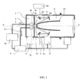
- the figure 1 schematically illustrates the general structure of an EUV source according to the invention.
- an irradiation chamber 1 a transmission chamber 2, an irradiation zone 3 located in the irradiation chamber 1, a diaphragm 4 provided in an intermediate wall 4a located between the irradiation chamber 1 and the chamber 2.
- the diaphragm 4 is oriented along an optical axis II which is the general axis according to which the EUV radiation emitted is recovered.
- Injection means 7, such as an inlet duct, make it possible to inject into the irradiation zone 3 a flow of radiation-generating material, which propagates in a direction II-II which is transverse to the optical axis II.
- the flow of radiation-generating material is recovered at the outlet of the irradiation zone 3 by a recycling pipe 8 which returns it by a primary pump 9 to a recycler 10 then re-injecting it into the irradiation zone 3 via the inlet pipe 7.
- a power laser radiation is produced which is preferably constituted by a plurality of power laser beams 5, 6, which converge towards the irradiation zone 3, and which strike the flow of material radiation generator for producing EUV radiation.
- the laser beams strike the flux of radiation-generating material on the face of the flow which is directed towards the diaphragm 4, and it is ensured that the diaphragm 4 is in the immediate vicinity of the irradiation zone 3.
- the EUV radiation emitted propagates preferentially through the diaphragm 4 to the transmission chamber 2, around the optical axis II.
- means such as a collector device 13 collect and condition the EUV radiation emitted by the radiation-generating material in the irradiation zone 3.
- the collecting device 13, located in the transmission chamber 2, may advantageously comprise one or more elliptical mirrors oriented along the optical axis II and having a first focus located in the irradiation zone 3.
- the elliptical mirrors reflect for the most part, the EUV radiation rays to direct them towards the second focus of the elliptical mirrors, the second focus that is placed in their area of use.
- An anti-debris device 14 may advantageously be provided in the transmission chamber 2 facing and near the diaphragm 4, to transmit the EUV radiation to the collector device 13 while preventing the passage of ions and other particles from the diaphragm 4 to the collecting device 13.
- An anti-debris device 14 may for example comprise a transverse flow of helium, argon or krypton downstream of the diaphragm 4.
- the radiation-generating material may for example be a xenon gas stream, a liquid sputtering xenon microdroplet stream, or a liquid xenon spaghetto.
- a tin target which has a better conversion ratio than xenon, can be envisioned, and thus can generate a higher intensity EUV radiation.
- the target may be a solid tin disc, or a flow of room temperature liquid tin alloy, such as an alloy of tin, indium and lead.
- the irradiation chamber 1 is a sealed chamber, surrounded by a sealed wall, and communicating with the transmission chamber 2 by the single diaphragm 4 which is of reduced size, for example of the order of 10 mm.
- the transmission chamber 2 is also a sealed chamber, surrounded by a sealed wall and communicating with the irradiation chamber 1 by the single diaphragm 4 of reduced size.
- the irradiation chamber 1 is connected to first vacuum generator means 11 which maintain a first pressure P1.
- first vacuum generator means 11 may comprise one or more turbomolecular secondary pumps 11 whose suction is connected to the irradiation chamber 1 and whose discharge is connected to the suction of the primary pump 9.
- the transmission chamber 2 is connected to second vacuum generation means 12 which maintain a second pressure P2.
- the second vacuum generating means 12 comprise one or more second turbomolecular secondary pumps 12 whose suction is connected to the transmission chamber 2 and whose discharge is connected to the suction of the primary pump 9.
- the second pressure P2, present in the transmission chamber 2 is smaller than the first pressure P1 present in the irradiation chamber 1, for the reason explained below.
- a vacuum is maintained at a first relatively high pressure P1, and it is arranged that the path length followed by the EUV radiation in the irradiation chamber 1 is very short. This is achieved by the fact that the diaphragm 4 is in the immediate vicinity of the irradiation zone 3, and thanks to the fact that the power laser radiation strikes the flow of radiation-generating material on the face which is opposite the diaphragm 4 .
- the transmission chamber 2 is maintained at a pressure P2 less than the first pressure P1 of the irradiation chamber 1. In this way, the absorption of the useful EUV radiation is reduced in its path through the transmission chamber 2.
- the second pressure P2 in the transmission chamber 2 is less than or equal to one-tenth of the first pressure P1 in the irradiation chamber 1.
- first pressure P1 of less than or equal to approximately 5 10 -3 millibars
- second pressure P2 less than or equal to 5 10 -4 millibars.
- the vacuum of 10 -3 millibars can be achieved in the irradiation chamber 1 by one or two first turbomolecular pumps 11 providing a total xenon pumping rate of about 3000 liters per second.
- the size of the first turbomolecular pump (s) 11 is thus compatible with the space requirement in photolithography installations for manufacturing semiconductor components.
- a simple diaphragm 4 of reduced size greatly reduces the flow of radiation-generating material which propagates towards the transmission chamber 2, according to a factor of about 10.
- the higher vacuum can be achieved and maintained in the transmission chamber 2 by one or two second turbomolecular pumps 12 whose total pumping rate of xenon is also about 3000 liters per second .
- the size of the second turbomolecular pump (s) 12 is thus reduced, and the assembly remains compatible with the space required in photolithography installations for semiconductor fabrication.
- the simple diaphragm 4 has the advantage of being multidirectional, that is to say to admit the passage of radiation that can be strongly oblique with respect to the optical axis I-I.
- the incident laser beams 5 and 6 can penetrate into the transmission chamber 2 by windows 5a and 6a, coming from laser sources such as the source 5b, they can be reflected by mirrors such as the mirrors 5c and 5d, to then propagate towards the diaphragm 4 outside the collecting device 13, to strike the surface of the flux of radiation-generating material which is, in the irradiation zone 3, in the immediate vicinity of the diaphragm 4.
- incident laser beams can be provided which penetrate directly into the irradiation chamber 1 upstream of the diaphragm 4, and which propagate towards the irradiation zone 3. along the intermediate wall 4a, upstream of the diaphragm 4.
- the diaphragm 4 is formed in the intermediate wall 4a which may advantageously have a conical top-shaped shape directed towards the irradiation zone 3.
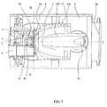
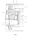
- FIGS. 2 and 3 illustrate in longitudinal section a first practical embodiment of an EUV source according to the present invention.
- a first secondary pump 11 is arranged laterally, and its suction orifice communicating directly with the irradiation chamber 1.
- a second secondary pump 12 is disposed laterally, and its suction port communicating directly with the transmission chamber 2 is distinguished.
- the irradiation zone 3 is located between an injector 15 connected to the inlet pipe 7 and a debarker 16 connected to the recycling pipe 8.
- the inlet pipe 7 and the pipe of recycling 8 are bent to connect respectively to the injector 15 and to the debarker 16, and they penetrate axially into the irradiation chamber 1.
- the irradiation zone is of short length, for example about 3 mm.
- the collector device 13 comprises for example two coaxial elliptical mirrors, namely an outer elliptical mirror 13a and an inner elliptical mirror 13b.
- the inner elliptical mirror 13b is set back from the diaphragm 4, as illustrated in the figures, while the outer elliptical mirror 13a is connected to a conical portion of the intermediate wall 4a separating the irradiation chamber 1 from the transmission chamber 2.
- the outer elliptical mirror 13a may advantageously be connected to a hyperbolic mirror surrounding the diaphragm 4, so as to optimize the amount of EUV radiation collected.
- the collector device 13 retrieves the EUV radiation emitted at a solid angle centered on the optical axis I-I and defined substantially by a cone of about 120 °.
- the transmission chamber 2 is closed downstream by a wall 2a transparent to the emitted EUV radiation, and possibly filtering to remove radiation wavelength greater than the desired radiation.
- the wall 2a isolates the atmosphere in the transmission chamber 2 from the atmosphere downstream of the wall 2a.
- the mirrors of the collecting device 13 have an elliptical shape, a first focus being located in the radiation zone 3, the second focus being located at the entrance 25 ( figure 5 ) of the optical system of an optical reducer mask repeater 26, which uses the radiation to process the semiconductor wafer.
- the EUV radiation is thus focused at the input 25 of the optical system 25, 26.
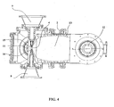
- FIG 4 there is shown a variant of the EUV radiation source of the figure 2 , variant in which the pipes 7 and 8 penetrate radially into the irradiation chamber 1, in line with the injector 15 and the debarker 16, respectively.
- the figure 5 illustrates the use of an EUV source according to the invention for the treatment of a semiconductor wafer.
- the radiation source is illustrated globally and identified by the reference A.
- the EUV B radiation is directed, through the entrance of the mask repeater, to a mask 20 supported by a mask support device 21.
- the mask 20 is reflective , and redirects the radiation, through the optical reducer 26 of the mask repeater, to a semiconductor wafer 22 itself supported by a wafer carrier 23.
- the semiconductor wafer 22 comprises for example a surface covered with a layer 24 that we want to treat by the EUV radiation, according to the pattern of the mask 20, with a reduction factor determined by the optical reducer 26.
Landscapes
- Physics & Mathematics (AREA)
- Engineering & Computer Science (AREA)
- Optics & Photonics (AREA)
- Plasma & Fusion (AREA)
- Chemical & Material Sciences (AREA)
- Nanotechnology (AREA)
- Theoretical Computer Science (AREA)
- Mathematical Physics (AREA)
- Crystallography & Structural Chemistry (AREA)
- General Physics & Mathematics (AREA)
- Exposure And Positioning Against Photoresist Photosensitive Materials (AREA)
- Exposure Of Semiconductors, Excluding Electron Or Ion Beam Exposure (AREA)
- X-Ray Techniques (AREA)
- Transition And Organic Metals Composition Catalysts For Addition Polymerization (AREA)
Applications Claiming Priority (2)
| Application Number | Priority Date | Filing Date | Title |
|---|---|---|---|
| FR0311280A FR2860385B1 (fr) | 2003-09-26 | 2003-09-26 | Source euv |
| FR0311280 | 2003-09-26 |
Publications (3)
| Publication Number | Publication Date |
|---|---|
| EP1528846A2 EP1528846A2 (fr) | 2005-05-04 |
| EP1528846A3 EP1528846A3 (fr) | 2005-06-08 |
| EP1528846B1 true EP1528846B1 (fr) | 2009-12-23 |
Family
ID=34307180
Family Applications (1)
| Application Number | Title | Priority Date | Filing Date |
|---|---|---|---|
| EP04292256A Expired - Lifetime EP1528846B1 (fr) | 2003-09-26 | 2004-09-20 | Source EUV |
Country Status (6)
| Country | Link |
|---|---|
| US (1) | US7095038B2 (enExample) |
| EP (1) | EP1528846B1 (enExample) |
| JP (1) | JP4690686B2 (enExample) |
| AT (1) | ATE453309T1 (enExample) |
| DE (1) | DE602004024754D1 (enExample) |
| FR (1) | FR2860385B1 (enExample) |
Cited By (1)
| Publication number | Priority date | Publication date | Assignee | Title |
|---|---|---|---|---|
| US9136794B2 (en) | 2011-06-22 | 2015-09-15 | Research Triangle Institute, International | Bipolar microelectronic device |
Families Citing this family (16)
| Publication number | Priority date | Publication date | Assignee | Title |
|---|---|---|---|---|
| US7439530B2 (en) | 2005-06-29 | 2008-10-21 | Cymer, Inc. | LPP EUV light source drive laser system |
| US7034320B2 (en) * | 2003-03-20 | 2006-04-25 | Intel Corporation | Dual hemispherical collectors |
| JP2005190904A (ja) * | 2003-12-26 | 2005-07-14 | Ushio Inc | 極端紫外光源 |
| US7482609B2 (en) | 2005-02-28 | 2009-01-27 | Cymer, Inc. | LPP EUV light source drive laser system |
| KR101396158B1 (ko) | 2006-05-16 | 2014-05-19 | 코닌클리케 필립스 엔.브이. | Euv 램프 및 연질 x-선 램프의 전환 효율을 증가시키는 방법, 및 euv 방사선 및 연질 x-선을 생성하는 장치 |
| US7655925B2 (en) | 2007-08-31 | 2010-02-02 | Cymer, Inc. | Gas management system for a laser-produced-plasma EUV light source |
| JP2011503869A (ja) * | 2007-11-08 | 2011-01-27 | エーエスエムエル ネザーランズ ビー.ブイ. | 放射システムおよび方法、ならびにスペクトル純度フィルタ |
| EP2083328B1 (en) * | 2008-01-28 | 2013-06-19 | Media Lario s.r.l. | Grazing incidence collector for laser produced plasma sources |
| EP2182412A1 (en) * | 2008-11-04 | 2010-05-05 | ASML Netherlands B.V. | Radiation source and lithographic apparatus |
| US8330131B2 (en) * | 2010-01-11 | 2012-12-11 | Media Lario, S.R.L. | Source-collector module with GIC mirror and LPP EUV light source |
| WO2013141578A1 (ko) * | 2012-03-20 | 2013-09-26 | 주식회사 에프에스티 | 플라즈마를 이용한 극자외선 발생장치 |
| NL2010965A (en) | 2012-06-22 | 2013-12-24 | Asml Netherlands Bv | Radiation source and lithographic apparatus. |
| US10880979B2 (en) | 2015-11-10 | 2020-12-29 | Kla Corporation | Droplet generation for a laser produced plasma light source |
| US9918375B2 (en) * | 2015-11-16 | 2018-03-13 | Kla-Tencor Corporation | Plasma based light source having a target material coated on a cylindrically-symmetric element |
| US10021773B2 (en) | 2015-11-16 | 2018-07-10 | Kla-Tencor Corporation | Laser produced plasma light source having a target material coated on a cylindrically-symmetric element |
| KR102024760B1 (ko) * | 2018-01-18 | 2019-09-25 | 한국원자력연구원 | 빔집속장치 |
Family Cites Families (9)
| Publication number | Priority date | Publication date | Assignee | Title |
|---|---|---|---|---|
| JPH01137543A (ja) * | 1987-11-24 | 1989-05-30 | Fujitsu Ltd | レーザ励起x線発生装置 |
| JPH0837096A (ja) * | 1994-07-26 | 1996-02-06 | Nikon Corp | X線発生装置 |
| JPH10221499A (ja) * | 1997-02-07 | 1998-08-21 | Hitachi Ltd | レーザプラズマx線源およびそれを用いた半導体露光装置並びに半導体露光方法 |
| US6541786B1 (en) * | 1997-05-12 | 2003-04-01 | Cymer, Inc. | Plasma pinch high energy with debris collector |
| JP2000089000A (ja) * | 1998-09-14 | 2000-03-31 | Nikon Corp | X線発生装置 |
| DE19962160C2 (de) * | 1999-06-29 | 2003-11-13 | Fraunhofer Ges Forschung | Vorrichtungen zur Erzeugung von Extrem-Ultraviolett- und weicher Röntgenstrahlung aus einer Gasentladung |
| US6304630B1 (en) * | 1999-12-24 | 2001-10-16 | U.S. Philips Corporation | Method of generating EUV radiation, method of manufacturing a device by means of said radiation, EUV radiation source unit, and lithographic projection apparatus provided with such a radiation source unit |
| JP4351413B2 (ja) * | 2002-03-05 | 2009-10-28 | 望月 孝晏 | レーザプラズマx線発生装置 |
| DE10251435B3 (de) * | 2002-10-30 | 2004-05-27 | Xtreme Technologies Gmbh | Strahlungsquelle zur Erzeugung von extrem ultravioletter Strahlung |
-
2003
- 2003-09-26 FR FR0311280A patent/FR2860385B1/fr not_active Expired - Fee Related
-
2004
- 2004-09-20 DE DE602004024754T patent/DE602004024754D1/de not_active Expired - Lifetime
- 2004-09-20 AT AT04292256T patent/ATE453309T1/de not_active IP Right Cessation
- 2004-09-20 EP EP04292256A patent/EP1528846B1/fr not_active Expired - Lifetime
- 2004-09-21 JP JP2004272681A patent/JP4690686B2/ja not_active Expired - Fee Related
- 2004-09-22 US US10/946,109 patent/US7095038B2/en not_active Expired - Fee Related
Non-Patent Citations (2)
| Title |
|---|
| FIEDOROWICZ H. ET AL.: "Strong extreme ultraviolet emission from a double-stream xenon/helium gas puff target irradiated with a Nd:YAG laser", OPTICS COMMUNICATIONS, vol. 184, 2000, pages 161 - 167, XP000421841 * |
| OESTREICH S. ET AL.: "Multilayer reflectance during exposure to EUV radiation", PROCEEDINGS OF THE SPIE, vol. 4646, pages 61 - 71, XP001059823 * |
Cited By (1)
| Publication number | Priority date | Publication date | Assignee | Title |
|---|---|---|---|---|
| US9136794B2 (en) | 2011-06-22 | 2015-09-15 | Research Triangle Institute, International | Bipolar microelectronic device |
Also Published As
| Publication number | Publication date |
|---|---|
| DE602004024754D1 (de) | 2010-02-04 |
| FR2860385B1 (fr) | 2007-06-01 |
| JP2005108834A (ja) | 2005-04-21 |
| ATE453309T1 (de) | 2010-01-15 |
| US7095038B2 (en) | 2006-08-22 |
| EP1528846A2 (fr) | 2005-05-04 |
| US20050072942A1 (en) | 2005-04-07 |
| JP4690686B2 (ja) | 2011-06-01 |
| EP1528846A3 (fr) | 2005-06-08 |
| FR2860385A1 (fr) | 2005-04-01 |
Similar Documents
| Publication | Publication Date | Title |
|---|---|---|
| EP1528846B1 (fr) | Source EUV | |
| EP1800188B1 (fr) | Dispositif de generation de lumiere dans l' extreme ultraviolet et application a une source de lithographie par rayonnement dans l'extreme ultraviolet | |
| EP2473315B1 (fr) | Tete de focalisation laser avec des lentilles en zns ayant une epaisseur aux bords d'au moins 5 mm ; installation et procede de coupage laser employant une telle tete de focalisation | |
| US4801352A (en) | Flowing gas seal enclosure for processing workpiece surface with controlled gas environment and intense laser irradiation | |
| EP1382230A1 (fr) | Procede et dispositif de generation de lumiere dans l'extreme ultraviolet notamment pour la lithographie | |
| JP2005108834A5 (enExample) | ||
| JP7544848B2 (ja) | ガス渦流を有するレーザ強化プラズマ光源 | |
| EP0520847B1 (fr) | Procédé de travail au laser dans une zone contaminée d'une installation nucléaire, et équipement pour sa mise en oeuvre | |
| WO2009027156A1 (fr) | Systeme d'analyse de gaz a basse pression par spectroscopie d'emission optique | |
| FR2604050A1 (fr) | Appareil et procede de creation d'un faisceau monoenergetique de particules et produits obtenus par leur mise en oeuvre | |
| EP1896197B1 (en) | Method of cleaning and after treatment of optical surfaces in an irradiation unit | |
| JP2010080409A (ja) | ガスフロー式spfを備えた極端紫外光源装置 | |
| WO2022226135A1 (en) | Laser-sustained plasma light source with reverse vortex flow | |
| TW202442034A (zh) | 高功率緊湊型真空紫外線(vuv)雷射維持電漿光源 | |
| EP1827511B1 (fr) | Decontamination laser de la surface d'une piece profilee | |
| FR2623820A1 (fr) | Depot en phase gazeuse par procede chimique a laser avec utilisation d'un faisceau a fibre optique | |
| EP2472305B1 (fr) | Système optique de focalisation pour installation de coupage avec laser solide | |
| EP1869695A2 (fr) | Dispositif micro-onde pour le traitement d'un flux par un rayonnement lumineux | |
| FR2548218A1 (fr) | Procede de depot de couches minces par reaction chimique en phase gazeuse utilisant deux rayonnements differents | |
| FR3083223A1 (fr) | Systeme de desinfection et de traitement d'eau par irradiation ultraviolette | |
| WO2025016632A1 (en) | Euv source vessel heated gas delivery apparatus and method | |
| EP4003635A1 (fr) | Systeme et procede de traitement par laser | |
| JPS61440A (ja) | 光反応装置における光源の汚染防止機構 | |
| FR2884350A1 (fr) | Source de photons comprenant une source rce equipee de miroirs | |
| FR2702852A1 (fr) | Procédé de traitement d'un faisceau laser par un milieu fluide non linéaire et cellule optique adaptée à sa mise en Óoeuvre. |
Legal Events
| Date | Code | Title | Description |
|---|---|---|---|
| PUAI | Public reference made under article 153(3) epc to a published international application that has entered the european phase |
Free format text: ORIGINAL CODE: 0009012 |
|
| PUAL | Search report despatched |
Free format text: ORIGINAL CODE: 0009013 |
|
| AK | Designated contracting states |
Kind code of ref document: A2 Designated state(s): AT BE BG CH CY CZ DE DK EE ES FI FR GB GR HU IE IT LI LU MC NL PL PT RO SE SI SK TR |
|
| AX | Request for extension of the european patent |
Extension state: AL HR LT LV MK |
|
| AK | Designated contracting states |
Kind code of ref document: A3 Designated state(s): AT BE BG CH CY CZ DE DK EE ES FI FR GB GR HU IE IT LI LU MC NL PL PT RO SE SI SK TR |
|
| AX | Request for extension of the european patent |
Extension state: AL HR LT LV MK |
|
| 17P | Request for examination filed |
Effective date: 20051208 |
|
| AKX | Designation fees paid |
Designated state(s): AT BE BG CH CY CZ DE DK EE ES FI FR GB GR HU IE IT LI LU MC NL PL PT RO SE SI SK TR |
|
| 17Q | First examination report despatched |
Effective date: 20060201 |
|
| RAP1 | Party data changed (applicant data changed or rights of an application transferred) |
Owner name: ALCATEL LUCENT |
|
| GRAP | Despatch of communication of intention to grant a patent |
Free format text: ORIGINAL CODE: EPIDOSNIGR1 |
|
| GRAS | Grant fee paid |
Free format text: ORIGINAL CODE: EPIDOSNIGR3 |
|
| GRAA | (expected) grant |
Free format text: ORIGINAL CODE: 0009210 |
|
| AK | Designated contracting states |
Kind code of ref document: B1 Designated state(s): AT BE BG CH CY CZ DE DK EE ES FI FR GB GR HU IE IT LI LU MC NL PL PT RO SE SI SK TR |
|
| REG | Reference to a national code |
Ref country code: GB Ref legal event code: FG4D Free format text: NOT ENGLISH |
|
| REG | Reference to a national code |
Ref country code: CH Ref legal event code: EP |
|
| REG | Reference to a national code |
Ref country code: IE Ref legal event code: FG4D |
|
| REF | Corresponds to: |
Ref document number: 602004024754 Country of ref document: DE Date of ref document: 20100204 Kind code of ref document: P |
|
| REG | Reference to a national code |
Ref country code: NL Ref legal event code: VDEP Effective date: 20091223 |
|
| PG25 | Lapsed in a contracting state [announced via postgrant information from national office to epo] |
Ref country code: SE Free format text: LAPSE BECAUSE OF FAILURE TO SUBMIT A TRANSLATION OF THE DESCRIPTION OR TO PAY THE FEE WITHIN THE PRESCRIBED TIME-LIMIT Effective date: 20091223 Ref country code: FI Free format text: LAPSE BECAUSE OF FAILURE TO SUBMIT A TRANSLATION OF THE DESCRIPTION OR TO PAY THE FEE WITHIN THE PRESCRIBED TIME-LIMIT Effective date: 20091223 |
|
| PG25 | Lapsed in a contracting state [announced via postgrant information from national office to epo] |
Ref country code: PL Free format text: LAPSE BECAUSE OF FAILURE TO SUBMIT A TRANSLATION OF THE DESCRIPTION OR TO PAY THE FEE WITHIN THE PRESCRIBED TIME-LIMIT Effective date: 20091223 Ref country code: SI Free format text: LAPSE BECAUSE OF FAILURE TO SUBMIT A TRANSLATION OF THE DESCRIPTION OR TO PAY THE FEE WITHIN THE PRESCRIBED TIME-LIMIT Effective date: 20091223 |
|
| PG25 | Lapsed in a contracting state [announced via postgrant information from national office to epo] |
Ref country code: AT Free format text: LAPSE BECAUSE OF FAILURE TO SUBMIT A TRANSLATION OF THE DESCRIPTION OR TO PAY THE FEE WITHIN THE PRESCRIBED TIME-LIMIT Effective date: 20091223 |
|
| REG | Reference to a national code |
Ref country code: IE Ref legal event code: FD4D |
|
| PG25 | Lapsed in a contracting state [announced via postgrant information from national office to epo] |
Ref country code: NL Free format text: LAPSE BECAUSE OF FAILURE TO SUBMIT A TRANSLATION OF THE DESCRIPTION OR TO PAY THE FEE WITHIN THE PRESCRIBED TIME-LIMIT Effective date: 20091223 Ref country code: BG Free format text: LAPSE BECAUSE OF FAILURE TO SUBMIT A TRANSLATION OF THE DESCRIPTION OR TO PAY THE FEE WITHIN THE PRESCRIBED TIME-LIMIT Effective date: 20100323 Ref country code: ES Free format text: LAPSE BECAUSE OF FAILURE TO SUBMIT A TRANSLATION OF THE DESCRIPTION OR TO PAY THE FEE WITHIN THE PRESCRIBED TIME-LIMIT Effective date: 20100403 Ref country code: EE Free format text: LAPSE BECAUSE OF FAILURE TO SUBMIT A TRANSLATION OF THE DESCRIPTION OR TO PAY THE FEE WITHIN THE PRESCRIBED TIME-LIMIT Effective date: 20091223 Ref country code: RO Free format text: LAPSE BECAUSE OF FAILURE TO SUBMIT A TRANSLATION OF THE DESCRIPTION OR TO PAY THE FEE WITHIN THE PRESCRIBED TIME-LIMIT Effective date: 20091223 Ref country code: PT Free format text: LAPSE BECAUSE OF FAILURE TO SUBMIT A TRANSLATION OF THE DESCRIPTION OR TO PAY THE FEE WITHIN THE PRESCRIBED TIME-LIMIT Effective date: 20100423 |
|
| PG25 | Lapsed in a contracting state [announced via postgrant information from national office to epo] |
Ref country code: SK Free format text: LAPSE BECAUSE OF FAILURE TO SUBMIT A TRANSLATION OF THE DESCRIPTION OR TO PAY THE FEE WITHIN THE PRESCRIBED TIME-LIMIT Effective date: 20091223 Ref country code: CZ Free format text: LAPSE BECAUSE OF FAILURE TO SUBMIT A TRANSLATION OF THE DESCRIPTION OR TO PAY THE FEE WITHIN THE PRESCRIBED TIME-LIMIT Effective date: 20091223 |
|
| PG25 | Lapsed in a contracting state [announced via postgrant information from national office to epo] |
Ref country code: CY Free format text: LAPSE BECAUSE OF FAILURE TO SUBMIT A TRANSLATION OF THE DESCRIPTION OR TO PAY THE FEE WITHIN THE PRESCRIBED TIME-LIMIT Effective date: 20091223 Ref country code: GR Free format text: LAPSE BECAUSE OF FAILURE TO SUBMIT A TRANSLATION OF THE DESCRIPTION OR TO PAY THE FEE WITHIN THE PRESCRIBED TIME-LIMIT Effective date: 20100324 Ref country code: IE Free format text: LAPSE BECAUSE OF FAILURE TO SUBMIT A TRANSLATION OF THE DESCRIPTION OR TO PAY THE FEE WITHIN THE PRESCRIBED TIME-LIMIT Effective date: 20091223 |
|
| PLBE | No opposition filed within time limit |
Free format text: ORIGINAL CODE: 0009261 |
|
| STAA | Information on the status of an ep patent application or granted ep patent |
Free format text: STATUS: NO OPPOSITION FILED WITHIN TIME LIMIT |
|
| PGFP | Annual fee paid to national office [announced via postgrant information from national office to epo] |
Ref country code: FR Payment date: 20101005 Year of fee payment: 7 |
|
| 26N | No opposition filed |
Effective date: 20100924 |
|
| PG25 | Lapsed in a contracting state [announced via postgrant information from national office to epo] |
Ref country code: DK Free format text: LAPSE BECAUSE OF FAILURE TO SUBMIT A TRANSLATION OF THE DESCRIPTION OR TO PAY THE FEE WITHIN THE PRESCRIBED TIME-LIMIT Effective date: 20091223 |
|
| PGFP | Annual fee paid to national office [announced via postgrant information from national office to epo] |
Ref country code: DE Payment date: 20100922 Year of fee payment: 7 |
|
| BERE | Be: lapsed |
Owner name: ALCATEL LUCENT Effective date: 20100930 |
|
| PG25 | Lapsed in a contracting state [announced via postgrant information from national office to epo] |
Ref country code: IT Free format text: LAPSE BECAUSE OF FAILURE TO SUBMIT A TRANSLATION OF THE DESCRIPTION OR TO PAY THE FEE WITHIN THE PRESCRIBED TIME-LIMIT Effective date: 20091223 |
|
| PG25 | Lapsed in a contracting state [announced via postgrant information from national office to epo] |
Ref country code: MC Free format text: LAPSE BECAUSE OF NON-PAYMENT OF DUE FEES Effective date: 20100930 |
|
| REG | Reference to a national code |
Ref country code: CH Ref legal event code: PL |
|
| GBPC | Gb: european patent ceased through non-payment of renewal fee |
Effective date: 20100920 |
|
| PG25 | Lapsed in a contracting state [announced via postgrant information from national office to epo] |
Ref country code: LI Free format text: LAPSE BECAUSE OF NON-PAYMENT OF DUE FEES Effective date: 20100930 Ref country code: BE Free format text: LAPSE BECAUSE OF NON-PAYMENT OF DUE FEES Effective date: 20100930 Ref country code: CH Free format text: LAPSE BECAUSE OF NON-PAYMENT OF DUE FEES Effective date: 20100930 |
|
| PG25 | Lapsed in a contracting state [announced via postgrant information from national office to epo] |
Ref country code: GB Free format text: LAPSE BECAUSE OF NON-PAYMENT OF DUE FEES Effective date: 20100920 |
|
| REG | Reference to a national code |
Ref country code: FR Ref legal event code: ST Effective date: 20120531 |
|
| PG25 | Lapsed in a contracting state [announced via postgrant information from national office to epo] |
Ref country code: DE Free format text: LAPSE BECAUSE OF NON-PAYMENT OF DUE FEES Effective date: 20120403 |
|
| REG | Reference to a national code |
Ref country code: DE Ref legal event code: R119 Ref document number: 602004024754 Country of ref document: DE Effective date: 20120403 |
|
| PG25 | Lapsed in a contracting state [announced via postgrant information from national office to epo] |
Ref country code: FR Free format text: LAPSE BECAUSE OF NON-PAYMENT OF DUE FEES Effective date: 20110930 |
|
| PG25 | Lapsed in a contracting state [announced via postgrant information from national office to epo] |
Ref country code: HU Free format text: LAPSE BECAUSE OF FAILURE TO SUBMIT A TRANSLATION OF THE DESCRIPTION OR TO PAY THE FEE WITHIN THE PRESCRIBED TIME-LIMIT Effective date: 20100624 Ref country code: LU Free format text: LAPSE BECAUSE OF NON-PAYMENT OF DUE FEES Effective date: 20100920 |
|
| PG25 | Lapsed in a contracting state [announced via postgrant information from national office to epo] |
Ref country code: TR Free format text: LAPSE BECAUSE OF FAILURE TO SUBMIT A TRANSLATION OF THE DESCRIPTION OR TO PAY THE FEE WITHIN THE PRESCRIBED TIME-LIMIT Effective date: 20091223 |
|
| REG | Reference to a national code |
Ref country code: FR Ref legal event code: CA Effective date: 20150521 |
|
| REG | Reference to a national code |
Ref country code: FR Ref legal event code: CA Effective date: 20150521 |