EP1528684B1 - Programmable phase-locked loop circuitry for programmable logic device - Google Patents
Programmable phase-locked loop circuitry for programmable logic device Download PDFInfo
- Publication number
- EP1528684B1 EP1528684B1 EP04256457A EP04256457A EP1528684B1 EP 1528684 B1 EP1528684 B1 EP 1528684B1 EP 04256457 A EP04256457 A EP 04256457A EP 04256457 A EP04256457 A EP 04256457A EP 1528684 B1 EP1528684 B1 EP 1528684B1
- Authority
- EP
- European Patent Office
- Prior art keywords
- programmable logic
- logic device
- digital
- input
- phase
- Prior art date
- Legal status (The legal status is an assumption and is not a legal conclusion. Google has not performed a legal analysis and makes no representation as to the accuracy of the status listed.)
- Not-in-force
Links
- 238000011144 upstream manufacturing Methods 0.000 claims 1
- 229920000729 poly(L-lysine) polymer Polymers 0.000 description 61
- 230000011664 signaling Effects 0.000 description 14
- 238000013461 design Methods 0.000 description 12
- 238000001914 filtration Methods 0.000 description 11
- 238000012545 processing Methods 0.000 description 10
- 239000000872 buffer Substances 0.000 description 8
- 238000004549 pulsed laser deposition Methods 0.000 description 6
- 238000010586 diagram Methods 0.000 description 5
- ORQBXQOJMQIAOY-UHFFFAOYSA-N nobelium Chemical compound [No] ORQBXQOJMQIAOY-UHFFFAOYSA-N 0.000 description 5
- 230000008901 benefit Effects 0.000 description 3
- 238000006243 chemical reaction Methods 0.000 description 3
- 230000000694 effects Effects 0.000 description 2
- 230000006870 function Effects 0.000 description 2
- 230000006855 networking Effects 0.000 description 2
- 230000000630 rising effect Effects 0.000 description 2
- 230000008859 change Effects 0.000 description 1
- 238000012937 correction Methods 0.000 description 1
- 238000005516 engineering process Methods 0.000 description 1
- 238000010348 incorporation Methods 0.000 description 1
- 238000012886 linear function Methods 0.000 description 1
- 238000012986 modification Methods 0.000 description 1
- 230000004048 modification Effects 0.000 description 1
- 230000002093 peripheral effect Effects 0.000 description 1
Images
Classifications
-
- H—ELECTRICITY
- H03—ELECTRONIC CIRCUITRY
- H03L—AUTOMATIC CONTROL, STARTING, SYNCHRONISATION OR STABILISATION OF GENERATORS OF ELECTRONIC OSCILLATIONS OR PULSES
- H03L7/00—Automatic control of frequency or phase; Synchronisation
- H03L7/06—Automatic control of frequency or phase; Synchronisation using a reference signal applied to a frequency- or phase-locked loop
- H03L7/08—Details of the phase-locked loop
- H03L7/085—Details of the phase-locked loop concerning mainly the frequency- or phase-detection arrangement including the filtering or amplification of its output signal
-
- H—ELECTRICITY
- H03—ELECTRONIC CIRCUITRY
- H03K—PULSE TECHNIQUE
- H03K19/00—Logic circuits, i.e. having at least two inputs acting on one output; Inverting circuits
- H03K19/02—Logic circuits, i.e. having at least two inputs acting on one output; Inverting circuits using specified components
- H03K19/173—Logic circuits, i.e. having at least two inputs acting on one output; Inverting circuits using specified components using elementary logic circuits as components
- H03K19/177—Logic circuits, i.e. having at least two inputs acting on one output; Inverting circuits using specified components using elementary logic circuits as components arranged in matrix form
- H03K19/17724—Structural details of logic blocks
- H03K19/17732—Macroblocks
-
- H—ELECTRICITY
- H03—ELECTRONIC CIRCUITRY
- H03K—PULSE TECHNIQUE
- H03K19/00—Logic circuits, i.e. having at least two inputs acting on one output; Inverting circuits
- H03K19/02—Logic circuits, i.e. having at least two inputs acting on one output; Inverting circuits using specified components
- H03K19/173—Logic circuits, i.e. having at least two inputs acting on one output; Inverting circuits using specified components using elementary logic circuits as components
- H03K19/177—Logic circuits, i.e. having at least two inputs acting on one output; Inverting circuits using specified components using elementary logic circuits as components arranged in matrix form
- H03K19/17736—Structural details of routing resources
-
- H—ELECTRICITY
- H03—ELECTRONIC CIRCUITRY
- H03L—AUTOMATIC CONTROL, STARTING, SYNCHRONISATION OR STABILISATION OF GENERATORS OF ELECTRONIC OSCILLATIONS OR PULSES
- H03L7/00—Automatic control of frequency or phase; Synchronisation
- H03L7/06—Automatic control of frequency or phase; Synchronisation using a reference signal applied to a frequency- or phase-locked loop
- H03L7/08—Details of the phase-locked loop
- H03L7/085—Details of the phase-locked loop concerning mainly the frequency- or phase-detection arrangement including the filtering or amplification of its output signal
- H03L7/089—Details of the phase-locked loop concerning mainly the frequency- or phase-detection arrangement including the filtering or amplification of its output signal the phase or frequency detector generating up-down pulses
- H03L7/0891—Details of the phase-locked loop concerning mainly the frequency- or phase-detection arrangement including the filtering or amplification of its output signal the phase or frequency detector generating up-down pulses the up-down pulses controlling source and sink current generators, e.g. a charge pump
-
- H—ELECTRICITY
- H03—ELECTRONIC CIRCUITRY
- H03L—AUTOMATIC CONTROL, STARTING, SYNCHRONISATION OR STABILISATION OF GENERATORS OF ELECTRONIC OSCILLATIONS OR PULSES
- H03L7/00—Automatic control of frequency or phase; Synchronisation
- H03L7/06—Automatic control of frequency or phase; Synchronisation using a reference signal applied to a frequency- or phase-locked loop
- H03L7/08—Details of the phase-locked loop
- H03L7/085—Details of the phase-locked loop concerning mainly the frequency- or phase-detection arrangement including the filtering or amplification of its output signal
- H03L7/093—Details of the phase-locked loop concerning mainly the frequency- or phase-detection arrangement including the filtering or amplification of its output signal using special filtering or amplification characteristics in the loop
-
- H—ELECTRICITY
- H03—ELECTRONIC CIRCUITRY
- H03L—AUTOMATIC CONTROL, STARTING, SYNCHRONISATION OR STABILISATION OF GENERATORS OF ELECTRONIC OSCILLATIONS OR PULSES
- H03L7/00—Automatic control of frequency or phase; Synchronisation
- H03L7/06—Automatic control of frequency or phase; Synchronisation using a reference signal applied to a frequency- or phase-locked loop
- H03L7/16—Indirect frequency synthesis, i.e. generating a desired one of a number of predetermined frequencies using a frequency- or phase-locked loop
- H03L7/18—Indirect frequency synthesis, i.e. generating a desired one of a number of predetermined frequencies using a frequency- or phase-locked loop using a frequency divider or counter in the loop
Definitions
- This invention relates to phase-locked loop circuitry including programmable components, and particularly to such circuitry, for use in a programmable logic device, where the programmable components can be used for other purposes.
- PLL phase-locked loop
- PLDs programmable logic devices
- a basic PLL includes a phase-frequency detector (“PFD”), a charge pump, a loop filter and a voltage-controlled oscillator (“VCO”), connected in series.
- the input or reference frequency is one input to the PFD.
- the output of the VCO which is the output of the PLL, is also fed back to another input of the PFD. If the feedback signal is not locked to the input reference signal, then the PFD output will be a signal (voltage) whose sign is indicative of whether the output leads or lags and whose magnitude is indicative of the amount of lead or lag. That signal is filtered by the charge pump and loop filter and is input to the VCO, causing the output frequency to change. Eventually, the output signal will lock to the phase of the input reference signal.
- the output signal also will lock to the frequency of the input reference signal, but in most PLLs, counters on the input and output of the PLL are used to divide the input frequency, while a counter/divider in the feedback loop is used to multiply the input frequency.
- the frequency of the output signal can be any rational multiple of the input frequency, but will be phase-locked to the input frequency.
- PLLs are thus relatively large and complex circuits, and providing PLLs on PLDs therefore either adds significant area to the PLD, or takes away area that could be used for programmable logic circuitry in a PLD of a given size. This is of particular concern because the PLLs that are provided may not be used in a particular user design, so that, as far as that user is concerned, the PLL circuitry is simply wasted. It would be desirable to be able to recapture that circuitry when it is not being used as a PLL.
- PLLs that are provided on a PLD typically are of a fixed design determined by the PLD manufacturer. However, for particular user designs, that fixed PLL design may not be suitable. Heretofore in such cases, the user had to either provide a PLL externally, or consume programmable logic resources on the PLD, which could have been put to other uses, to construct a PLL meeting the particular needs of the user design. It would be desirable to be able to provide more flexible PLL circuitry on a PLD.
- the Patent publication US 6211739-B1 discloses an FPGA comprising a PLL with a loop filter implemented by a microprocessor.
- the present invention consists in a programmable logic device comprising a phase-locked loop circuit and another portion, said phase-locked loop circuit having an input terminal for receiving an input signal having a reference frequency and an output terminal for outputting an output frequency phase-locked to said reference frequency, and comprising: an oscillator for producing said output frequency; and a feedback path feeding said oscillator, said feedback path accepting as inputs said reference frequency and said output frequency, and causing said oscillator to drive said output frequency to a phase-frequency lock with said reference frequency, said feedback path comprising at least one component connected therein; characterized in that: at least one of said at least one component is also provided with programmable connections to said another portion of said programmable logic device for operation of said another portion of said programmable logic device with said at least one of said at least one component; whereby when said phase-locked loop circuit is not in use in said programmable logic device, said at least one of said at least one component can be connected via said connections for use by said another portion of said programmable logic device; and whereby when
- Embodiments of the invention provide phase-locked loop circuitry on a programmable logic device that is both more flexible than previously known PLL circuits on PLDs and able to be, at least in part, recaptured when not being used as a PLL. This may be accomplished by replacing the conventional analog filter components in the control loop of the PLL with a series of components which may be adjustable or programmable, and which may have connections to other portions of the PLD.
- the adjustability of the components makes the PLL more flexible than previously known fixed PLL implementations. Moreover, if the components have connections to other portions of the PLD, then in some circumstances, if the user design calls for more complex filtering than is provided in the PLL circuitry, even with adjustable components, then more complex filter components can be implemented elsewhere in the PLD and substituted for portions of the PLL circuitry.
- those components that are particular to PLLs -- i.e., those components that make it preferable to provide dedicated PLL circuitry on a PLD rather than expect users to create PLLs from programmable logic -- are provided in their conventional fixed analog form. These include, in particular, the phase-frequency detector and the voltage-controlled oscillator.
- one or more components of the analog filtering path -- i.e., the charge pump and loop filter -- may be provided in digital form, and may be adjustable or programmable.
- providing the filtering components in digital form may allow more elaborate filtering schemes to be used, and also may allow for improved noise rejection in the feedback loop.
- these digital components may be provided with some adjustability, allowing them to be programmed by the user to achieve some of these advantages.
- the analog filtering components -- i.e., the charge pump and loop filter -- may be replaced by an analog front end, an analog-to-digital converter ("ADC"), a digital signal processor (“DSP”) and a digital-to-analog converter (“DAC").
- ADC analog-to-digital converter
- DSP digital signal processor
- DAC digital-to-analog converter
- the analog front end may resemble a conventional charge pump, so that effectively only the loop filter is replaced by the ADC, DSP and DAC.
- connections from a first external pin to an input of the ADC from an output of the ADC to the programmable logic components of the PLD (i.e., to one or more of the programmable logic regions of the PLD, or alternatively to the general purpose interconnect of the PLD, allowing the ADC output to be routed to any programmable logic region), from the programmable logic components of the PLD to an input of the DAC, and from an output of the DAC to a second external pin.
- an external signal can be routed from the first external pin to the ADC and thence to the programmable logic components, thereby providing the user with an ADC through which to route an external input signal prior to processing by digital logic.
- an internal signal can be routed out of the PLD and back in through the ADC if an ADC is needed for intermediate conversion of an analog signal to digital format.
- a digital output signal can be routed from the programmable logic components to the DAC and thence to the second external pin as an analog output signal.
- a digital signal can be routed out of the PLD through the DAC and back in through the other pin if a DAC is needed for intermediate conversion of a digital signal to analog format.
- the ADC, DSP and DAC can be used as a unit.
- An analog signal to be processed by the DSP can be input on the first terminal and output on the second terminal.
- the user can use this block of circuitry independently of the remainder of the PLD, or, by connecting the first and second terminals to other terminals, can route signals out of the programmable logic core of the PLD into the ADC/DSP/DAC block and then back into the programmable logic core.
- the user can use the ADC/DSP/DAC block either as a front end for processing an input signal before inputting it to the programmable logic core of the PLD, or as a back end for processing an output signal from the programmable logic core.
- connections from the ADC output to the PLD core and from the PLD core to the DAC input can be used when the PLL is in use to route the PLL feedback signal through an alternate DSP or other filter constructed in the PLD core according to a user design which may require more complex, or simply different, filtering than is provided by the "standard" DSP.
- an input to the DSP from the PLD core, and an output from the DSP to the PLD core can be provided to allow the DSP (without the ADC or DAC) to be used by user logic in the PLD core (e.g., in cases where the user logic is already in digital mode, or where the user constructs a more elaborate, or simply different, ADC and/or DAC).
- VCO voltage-controlled oscillator
- CCO current-controlled oscillator
- analog PFD could be replaced by one or more digital components, eliminating the need for the ADC.
- DSP and DAC could be reusable, separately or as a unit, in the manner described above for the embodiment that includes an ADC.
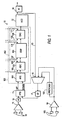
- FIG. 1 is a block diagram of a preferred embodiment of a phase-locked loop circuit according to the present invention
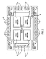
- FIG. 2 is a block diagram of an exemplary programmable logic device incorporating a phase-locked loop circuit according to the present invention
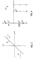
- FIG. 3 is a graph showing preferred input/output characteristics of the analog front end of the phase-locked loop circuit of FIG. 1 ;
- FIG. 4 is a schematic diagram of a preferred embodiment of the analog front end of the phase-locked loop circuit of FIG. 1 ;
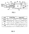
- FIG. 5 is a block diagram of an alternate preferred embodiment of a portion of the phase-locked loop circuit of FIG. 1 ;
- FIG. 6 is a table showing preferred characteristics of the phase-frequency detector in the embodiment of FIG. 5 ;
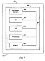
- FIG. 7 is a simplified block diagram of an illustrative system employing a programmable logic device incorporating a phase-locked loop in accordance with the present invention.
- the present invention improves resource utilization in PLDs having PLLs incorporated thereon, by allowing portions of unused PLLs to be used for other functions by the programmable logic core of the PLD, and also by allowing portions of the programmable logic core to be substituted for portions of the PLLs. This is achieved by breaking down the conventional analog filtering elements of a PLL feedback loop into blocks that may include digital circuitry and that may be programmable or adjustable, and by providing connections between individual ones of those blocks and the programmable logic core of the PLD.
- FIGS. 1-6 The invention will now be described with reference to FIGS. 1-6 .
- a phase-locked loop 10 preferably includes a phase-frequency detector (PFD) 11 and voltage-controlled oscillator (VCO) 12, which may (but need not) be conventional.
- the output of VCO 12 is fed back to PFD 11 through feedback loop 13, to which a reference signal is also input.
- a prescale counter 14 may be located between input buffer 15 and PFD 11 to divide the input reference frequency by a preloaded integer value N.
- a postscale counter 16 may be provided to divide the output frequency by a preloaded integer value K.
- a feedback scale counter 17 may be provided in feedback loop 13 to divide the frequency of the feedback signal by a preloaded integer value M, with the effect of multiplying the output frequency by M.
- counters 14, 16 and 17 have the effect of multiplying the input frequency by M/(NK). Without counters 14, 16 and 17 a PLL would also be a "frequency-locked loop," because in addition to the output phase being the same as the input phase, the output frequency'would be the same as the input frequency.
- multiplexer 18 and input buffer 19 are provided.
- Multiplexer 18 is located in feedback loop 13 after VCO 12 and before feedback scale counter 17, thereby allowing a signal other than the output of VCO 12 to be fed back through counter 17 to PFD 11.
- prescale divider 190 is also provided, allowing multiplexer 18 to select from among the output of VCO 12, an input from input buffer 19, or an input from input buffer 19 after frequency division by prescale divider 190.
- Each of input buffers 15, 19 is shown with two input terminals 150. It is contemplated that buffers 15, 19 allow for the use of differential signaling schemes (e.g., Low Voltage Differential Signaling, or "LVDS"). However, such signaling schemes form no part of the present invention, which may be used with either differential or single-ended signaling schemes.
- differential signaling schemes e.g., Low Voltage Differential Signaling, or "LVDS"
- LVDS Low Voltage Differential Signaling
- PLL 10 preferably includes digital filter 100.
- Digital filter 100 preferably includes an analog front end (AFE) 101, which preferably replaces the charge pump, and a digital filter element 102, which preferably replaces the loop filter.
- AFE 101 and filter element 102 preferably are adjustable and/or programmable to allow a user to select different filter characteristics.
- digital filter element 102 includes, in series, an analog-to-digital converter (ADC) 103, a digital signal processor (DSP) 104 and a digital-to-analog converter (DAC) 105.
- ADC analog-to-digital converter
- DSP digital signal processor
- DAC digital-to-analog converter
- each also preferably has respective inputs 106, 107, 108, and respective outputs 109, 110, 111, from or to, respectively, other parts of a device, such as PLD 20 ( FIG. 2 ), of which PLL 10 may be a part.
- the other part of the device may be an input/output pin, or may be other circuitry on the device, while for the other inputs and outputs 107-110, the other part of the device is preferably other circuitry on the device, although it could be an input/output pin as well.
- the resolution and conversion range of ADC 103 preferably are selected so that the desired phase error correction and phase detector pull-in range can be achieved.
- PLD 20 shown schematically in FIG. 2 , is one example of a device of which PLL 10 may be a component.
- PLL 20 preferably includes a plurality of programmable logic regions 21 accessible to programmable interconnect structure 22.
- the layout of regions 21 and interconnect structure 22 as shown in FIG. 2 is intended to be schematic only, as many actual arrangements are known to, or may be created by, those of ordinary skill in the art.
- the locations of PLLs 10 on PLD 20 are shown schematically only, as PLLs 10 actually may be located anywhere on PLD 20, including inside logic regions 21, in accordance with the design of a particular PLD 20.
- PLD 20 also includes a plurality of input/output (I/O) regions 23.
- I/O regions 23 preferably are programmable, allowing the selection of one of a number of possible I/O signaling schemes, which may include differential and/or non-differential signaling schemes.
- I/O regions 23 may be fixed, each allowing only a particular signaling scheme.
- a number of different types of fixed I/O regions 23 may be provided, so that while an individual region 23 does not allow a selection of signaling schemes, nevertheless PLD 20 as a whole does allow such a selection.
- PLL 10 is designed to allow connection to circuitry external to PLL 10, including circuitry on PLD 20, that uses differential signaling schemes as discussed above.
- DSP 104 as part of digital filter 100 gives digital filter 100 a degree of programmability, and therefore flexibility, not heretofore found in PLLs. Not only does the programmability of DSP 104 allow adjustment of the filtering characteristics of PLL 10 itself, but it also provides a programmable DSP capability on PLD 20. If digital signals are present on PLD 20, they can be processed, by way of input 107 and output 110, by DSP 104 of a PLL 10 that is not being used. Analog signals similarly can be processed, by way of input 106 and output 111, by DSP 104 of a PLL 10 that is not being used. By combining input 106 and output 110, analog signals can be processed by DSP 104 and allowed to remain in digital mode after processing. By combining input 107 and output 111, digital signals can be processed by DSP 104 and converted to analog mode after processing.
- ADC 103 and DAC 105 are available for standalone use via input 106 and output 109, or input 108 and output 111, respectively.
- a filter circuit may be constructed according to the user design in one of programmable logic regions 21.
- a more complex DSP may be built-in elsewhere on PLD 20, as disclosed, e.g., in commonlyassigned U.S. Patent 6,538,470 .
- AFE 101 has the output characteristic shown in FIG. 3 .
- the output is a voltage 30 that is a linear function of the phase error indicated by PFD 11.
- the maximum output voltage of AFE 101 may be limited. For example, ordinarily the output voltage cannot exceed the power supply voltage, and therefore the output voltage may saturate at a certain value, as indicated in phantom at 31, no matter how much larger the phase error becomes.
- AFE circuit 40 is substantially identical to a conventional charge pump as used in conventional PLLs.
- PFD 11 generates an UP signal, meaning that the phase must be advanced
- switch 41 will close and current will be sourced from current source 43 to create a positive voltage on resistor 44 that is passed to digital filter 102.
- PFD 11 generates a DOWN signal, meaning that the phase must be retarded
- switch 42 will close and current will be sunk into current source 45 to create a negative voltage on resistor 44 that is passed to digital filter element 102.
- any analog front end having the desired phase-versus-voltage characteristic can be used as AFE 101.
- a digital PFD 50 and an up/down counter 51 could be provided as shown in FIG. 5 .
- digital PFD 50 provides simple UP and DOWN signals 52, 53.
- the magnitude of the required phase advance or retardation is indicated not by the magnitude of signals 52, 53, but by how often signals 52, 53 occur, as counted by up/down counter 51.
- the output of digital PFD 50 is shown in the table in FIG. 6 . As shown, if the feedback signal, FBCLK, is low on a rising edge of the reference signal, REFCLK, the UP signal goes high, signaling that FBCLK must be advanced. If the reference signal, REFCLK, is low on a rising edge of the feedback signal, FBCLK, the DOWN signal goes high, signaling that FBCLK must be retarded.
- digital filter 500 (similar to filter 100) preferably includes counter 51 and digital filter element 502.
- Digital filter element 502 preferably is similar to digital filter element 102, except that it does not include an ADC. However, it does preferably include a DSP 504 for processing counter output signals 54, 55, and a DAC 505 for converting digital DSP output 56 to an analog signal 57.
- DSP 504 and DAC 505 include leads 507, 508, 510 and 511, allowing reuse of DSP 504 and DAC 505 either individually or as a unit, just as leads 107, 108, 110, 111 allow reuse of DSP 104 and DAC 105.
- a programmable logic device (PLD) 20 incorporating a PLL 10 according to the present invention may be used in many kinds of electronic devices.
- Data processing system 900 may include one or more of the following components: a processor 901; memory 902; I/O circuitry 903; and peripheral devices 904. These components are coupled together by a system bus 905 and are populated on a circuit board 906 which is contained in an end-user system 907.
- System 900 can be used in a wide variety of applications, such as computer networking, data networking, instrumentation, video processing, digital signal processing, or any other application where the advantage of using programmable or reprogrammable logic is desirable.
- PLD 20 can be used to perform a variety of different logic functions.
- PLD 20 can be configured as a processor or controller that works in cooperation with processor 901.
- PLD 20 may also be used as an arbiter for arbitrating access to a shared resources in system 900.
- PLD 20 can be configured as an interface between processor 901 and one of the other components in system 900. It should be noted that system 900 is only exemplary, and that the true scope of the invention should be indicated by the following claims.
Landscapes
- Physics & Mathematics (AREA)
- Mathematical Physics (AREA)
- Engineering & Computer Science (AREA)
- Computer Hardware Design (AREA)
- Computing Systems (AREA)
- General Engineering & Computer Science (AREA)
- Computer Networks & Wireless Communication (AREA)
- Stabilization Of Oscillater, Synchronisation, Frequency Synthesizers (AREA)
- Semiconductor Integrated Circuits (AREA)
- Design And Manufacture Of Integrated Circuits (AREA)
Applications Claiming Priority (2)
| Application Number | Priority Date | Filing Date | Title |
|---|---|---|---|
| US691152 | 2003-10-21 | ||
| US10/691,152 US6924678B2 (en) | 2003-10-21 | 2003-10-21 | Programmable phase-locked loop circuitry for programmable logic device |
Publications (3)
| Publication Number | Publication Date |
|---|---|
| EP1528684A2 EP1528684A2 (en) | 2005-05-04 |
| EP1528684A3 EP1528684A3 (en) | 2005-11-09 |
| EP1528684B1 true EP1528684B1 (en) | 2011-07-27 |
Family
ID=34423318
Family Applications (1)
| Application Number | Title | Priority Date | Filing Date |
|---|---|---|---|
| EP04256457A Not-in-force EP1528684B1 (en) | 2003-10-21 | 2004-10-20 | Programmable phase-locked loop circuitry for programmable logic device |
Country Status (4)
| Country | Link |
|---|---|
| US (3) | US6924678B2 (zh) |
| EP (1) | EP1528684B1 (zh) |
| JP (1) | JP2005209159A (zh) |
| CN (1) | CN1610261B (zh) |
Families Citing this family (27)
| Publication number | Priority date | Publication date | Assignee | Title |
|---|---|---|---|---|
| US7075365B1 (en) | 2004-04-22 | 2006-07-11 | Altera Corporation | Configurable clock network for programmable logic device |
| US7385429B1 (en) * | 2005-05-31 | 2008-06-10 | Altera Corporation | Charge pump with reduced current mismatch |
| JP4982110B2 (ja) * | 2005-06-02 | 2012-07-25 | 株式会社東芝 | 半導体集積回路装置 |
| US7523289B2 (en) | 2005-09-30 | 2009-04-21 | Spectra Logic Corporation | Random access storage system capable of performing storage operations intended for alternative storage devices |
| CN100459433C (zh) * | 2005-10-10 | 2009-02-04 | 华为技术有限公司 | 数字逻辑锁相环的实现装置 |
| US7590207B1 (en) | 2005-10-20 | 2009-09-15 | Altera Corporation | Modular serial interface in programmable logic device |
| US7436228B1 (en) | 2005-12-22 | 2008-10-14 | Altera Corporation | Variable-bandwidth loop filter methods and apparatus |
| US7764207B2 (en) * | 2006-03-31 | 2010-07-27 | Nihon Dempa Kogyo Co., Ltd. | Digital processor |
| US20070230109A1 (en) * | 2006-03-31 | 2007-10-04 | Spectra Logic Corporation | High density array system with active storage blades |
| US7728674B1 (en) | 2006-05-19 | 2010-06-01 | Altera Corporation | Voltage-controlled oscillator methods and apparatus |
| JP4213172B2 (ja) * | 2006-06-19 | 2009-01-21 | 日本電波工業株式会社 | Pll発振回路 |
| US7508609B2 (en) * | 2006-10-25 | 2009-03-24 | Spectra Logic Corporation | Formatted storage media providing space for encrypted text and dedicated space for clear text |
| US7619451B1 (en) * | 2007-02-03 | 2009-11-17 | Altera Corporation | Techniques for compensating delays in clock signals on integrated circuits |
| US7642861B2 (en) * | 2007-09-27 | 2010-01-05 | Infineon Technologies | Locked loop system |
| TWI339951B (en) * | 2007-11-14 | 2011-04-01 | Via Tech Inc | Chip sets and clock generation methods thereof |
| JP2009159038A (ja) * | 2007-12-25 | 2009-07-16 | Hitachi Ltd | Pll回路 |
| KR20090074412A (ko) * | 2008-01-02 | 2009-07-07 | 삼성전자주식회사 | 분주회로 및 이를 이용한 위상 동기 루프 |
| KR101023827B1 (ko) * | 2008-02-05 | 2011-03-22 | 시스레인 주식회사 | 국부 발진기 |
| CN101677236B (zh) * | 2008-09-19 | 2013-02-13 | 阿尔特拉公司 | 用于调整反馈时钟信号的数字环路滤波器和方法 |
| US8984421B2 (en) * | 2009-07-01 | 2015-03-17 | Thales Avionics, Inc. | Aircraft crew user interface for an aircraft entertainment system |
| JP5841993B2 (ja) * | 2011-03-07 | 2016-01-13 | パナソニック株式会社 | Pll回路、キャリブレーション方法及び無線通信端末 |
| US9442478B2 (en) | 2011-11-30 | 2016-09-13 | Infineon Technologies Ag | Systems, circuits and a method for generating a configurable feedback |
| US8659144B1 (en) * | 2011-12-15 | 2014-02-25 | Marvell International Ltd. | Power and ground planes in package substrate |
| KR101462756B1 (ko) * | 2013-01-28 | 2014-11-21 | 강원대학교산학협력단 | 동적 전압 주파수 변환 장치 |
| JP5904148B2 (ja) * | 2013-03-25 | 2016-04-13 | 富士ゼロックス株式会社 | 再構成可能回路、画像形成装置及びプログラム |
| CN106301748A (zh) * | 2015-05-19 | 2017-01-04 | 中兴通讯股份有限公司 | 时钟输出方法及装置 |
| CN110830041B (zh) * | 2019-11-25 | 2023-09-15 | 上海华力微电子有限公司 | 占空比50%的连续整数分频器及包括其的锁相环电路 |
Citations (1)
| Publication number | Priority date | Publication date | Assignee | Title |
|---|---|---|---|---|
| US6211739B1 (en) * | 1997-06-03 | 2001-04-03 | Cypress Semiconductor Corp. | Microprocessor controlled frequency lock loop for use with an external periodic signal |
Family Cites Families (76)
| Publication number | Priority date | Publication date | Assignee | Title |
|---|---|---|---|---|
| US3473160A (en) | 1966-10-10 | 1969-10-14 | Stanford Research Inst | Electronically controlled microelectronic cellular logic array |
| US4494021A (en) | 1982-08-30 | 1985-01-15 | Xerox Corporation | Self-calibrated clock and timing signal generator for MOS/VLSI circuitry |
| US4719593A (en) | 1984-07-09 | 1988-01-12 | Advanced Micro Devices, Inc. | Apparatus for generating digital timing waveforms |
| US4633488A (en) | 1984-11-13 | 1986-12-30 | Digital Equipment Corporation | Phase-locked loop for MFM data recording |
| US4858178A (en) | 1986-09-30 | 1989-08-15 | Texas Instruments Incorporated | Programmable sequence generator |
| US5133064A (en) | 1987-04-27 | 1992-07-21 | Hitachi, Ltd. | Data processing system generating clock signal from an input clock, phase locked to the input clock and used for clocking logic devices |
| JPH0770168B2 (ja) | 1987-08-17 | 1995-07-31 | 日本電気株式会社 | 磁気ディスク装置用pll回路 |
| JPH01137646A (ja) | 1987-11-25 | 1989-05-30 | Hitachi Ltd | 集積回路 |
| US5349544A (en) | 1988-06-15 | 1994-09-20 | Advanced Micro Devices, Inc. | Programmable system synchronizer |
| US4959646A (en) | 1988-06-17 | 1990-09-25 | Dallas Semiconductor Corporation | Dynamic PLA timing circuit |
| US4868522A (en) | 1988-12-13 | 1989-09-19 | Gazelle Microcircuits, Inc. | Clock signal distribution device |
| EP0416930B1 (en) | 1989-09-08 | 1997-11-12 | Fujitsu Limited | Encoding and decoding circuit for run-length-limited coding |
| US5075575A (en) | 1989-12-11 | 1991-12-24 | Fuji Photo Film Co., Ltd. | Externally synchronized programmable device |
| US5204555A (en) | 1990-04-05 | 1993-04-20 | Gazelle Microcircuits, Inc. | Logic array having high frequency internal clocking |
| US5072195A (en) | 1990-04-05 | 1991-12-10 | Gazelle Microcircuits, Inc. | Phase-locked loop with clamped voltage-controlled oscillator |
| US5239213A (en) | 1990-04-30 | 1993-08-24 | Advanced Micro Devices, Inc. | Precision timing control programmable logic device |
| US5079519A (en) | 1991-02-14 | 1992-01-07 | Notorola, Inc. | Digital phase lock loop for a gate array |
| US5121014A (en) | 1991-03-05 | 1992-06-09 | Vlsi Technology, Inc. | CMOS delay circuit with controllable delay |
| US5208557A (en) | 1992-02-18 | 1993-05-04 | Texas Instruments Incorporated | Multiple frequency ring oscillator |
| JP2792801B2 (ja) | 1992-12-28 | 1998-09-03 | 三菱電機株式会社 | 半導体集積回路並びにその設計方法及び製造方法 |
| US5355035A (en) | 1993-01-08 | 1994-10-11 | Vora Madhukar B | High speed BICMOS switches and multiplexers |
| DE69411217T2 (de) | 1993-04-05 | 1999-02-04 | Philips Electronics Nv | Verzögerungsschaltung zum Verzögern von differentiellen Signalen |
| JP3033654B2 (ja) | 1993-08-23 | 2000-04-17 | 日本電気株式会社 | Pll周波数シンセサイザ |
| JPH0774596A (ja) | 1993-08-31 | 1995-03-17 | Mitsubishi Electric Corp | リング発振器 |
| FR2709624B1 (fr) | 1993-08-31 | 1995-11-17 | Sgs Thomson Microelectronics | Synthétiseur de fréquence. |
| US5394116A (en) | 1993-12-29 | 1995-02-28 | At&T Corp. | Fractional phase shift ring oscillator arrangement |
| US5506878A (en) | 1994-07-18 | 1996-04-09 | Xilinx, Inc. | Programmable clock having programmable delay and duty cycle based on a user-supplied reference clock |
| JP2710214B2 (ja) | 1994-08-12 | 1998-02-10 | 日本電気株式会社 | フェーズロックドループ回路 |
| US5815016A (en) | 1994-09-02 | 1998-09-29 | Xilinx, Inc. | Phase-locked delay loop for clock correction |
| US5646564A (en) | 1994-09-02 | 1997-07-08 | Xilinx, Inc. | Phase-locked delay loop for clock correction |
| JPH0879074A (ja) | 1994-09-05 | 1996-03-22 | Mitsubishi Electric Corp | フェーズ・ロックド・ループ回路 |
| US5777360A (en) | 1994-11-02 | 1998-07-07 | Lsi Logic Corporation | Hexagonal field programmable gate array architecture |
| US5742180A (en) | 1995-02-10 | 1998-04-21 | Massachusetts Institute Of Technology | Dynamically programmable gate array with multiple contexts |
| US5744991A (en) * | 1995-10-16 | 1998-04-28 | Altera Corporation | System for distributing clocks using a delay lock loop in a programmable logic circuit |
| US5656959A (en) | 1995-11-24 | 1997-08-12 | International Microcircuits, Inc. | Clock synthesizer dual function pin system and method therefor |
| KR970029314A (ko) | 1995-11-27 | 1997-06-26 | 윌리엄 이. 힐러 | 화상 제어 신호를 화소 클럭 신호로 인코딩하는 시스템 |
| US5691669A (en) | 1996-01-11 | 1997-11-25 | Hewlett-Packard Co. | Dual adjust current controlled phase locked loop |
| JP2919335B2 (ja) * | 1996-02-06 | 1999-07-12 | 埼玉日本電気株式会社 | Afc型発振回路 |
| US5699020A (en) | 1996-04-11 | 1997-12-16 | Altera Corporation | Phase latched differential charge pump circuit and method |
| US5900757A (en) | 1996-05-01 | 1999-05-04 | Sun Microsystems, Inc. | Clock stopping schemes for data buffer |
| FR2750268B1 (fr) | 1996-06-19 | 1998-07-31 | Bull Sa | Procede pour obtenir un signal a frequence variable et cellule a retard variable adaptee a la mise en oeuvre de ce procede |
| US5642082A (en) | 1996-06-20 | 1997-06-24 | Altera Corporation | Loop filter level detection circuit and method |
| US5847617A (en) | 1996-08-12 | 1998-12-08 | Altera Corporation | Variable-path-length voltage-controlled oscillator circuit |
| US5889436A (en) | 1996-11-01 | 1999-03-30 | National Semiconductor Corporation | Phase locked loop fractional pulse swallowing frequency synthesizer |
| JPH10215156A (ja) | 1997-01-29 | 1998-08-11 | Nec Corp | 遅延時間可変装置 |
| US5974105A (en) | 1997-03-13 | 1999-10-26 | Industrial Technology Research Institute | High frequency all digital phase-locked loop |
| US5987543A (en) | 1997-08-29 | 1999-11-16 | Texas Instruments Incorporated | Method for communicating digital information using LVDS and synchronous clock signals |
| US6144242A (en) | 1997-09-04 | 2000-11-07 | Silicon Image, Inc. | Controllable delays in multiple synchronized signals for reduced electromagnetic interference at peak frequencies |
| US6043677A (en) | 1997-10-15 | 2000-03-28 | Lucent Technologies Inc. | Programmable clock manager for a programmable logic device that can implement delay-locked loop functions |
| US6104222A (en) | 1997-12-17 | 2000-08-15 | Sony Corporation | Flexible phase locked loop system |
| US6141394A (en) * | 1997-12-22 | 2000-10-31 | Philips Electronics North America Corporation | Fractional-N frequency synthesizer with jitter compensation |
| US5970110A (en) | 1998-01-09 | 1999-10-19 | Neomagic Corp. | Precise, low-jitter fractional divider using counter of rotating clock phases |
| US6157266A (en) | 1998-02-12 | 2000-12-05 | Hewlett-Packard Company | Delay elements arranged for a signal controlled oscillator |
| US5999025A (en) | 1998-03-27 | 1999-12-07 | Xilinx, Inc. | Phase-locked loop architecture for a programmable logic device |
| US6069506A (en) | 1998-05-20 | 2000-05-30 | Micron Technology, Inc. | Method and apparatus for improving the performance of digital delay locked loop circuits |
| US6069507A (en) | 1998-05-22 | 2000-05-30 | Silicon Magic Corporation | Circuit and method for reducing delay line length in delay-locked loops |
| US6014048A (en) | 1998-05-27 | 2000-01-11 | Advanced Micro Devices, Inc. | Clock generator with multiple feedback paths including a delay locked loop path |
| US6249189B1 (en) | 1998-08-05 | 2001-06-19 | National Science Council Of Republic Of China | Frequency synthesizer accomplished by using multiphase reference signal source |
| JP2990171B1 (ja) | 1998-08-24 | 1999-12-13 | 日本電気アイシーマイコンシステム株式会社 | Pll回路とその制御方法 |
| US6448820B1 (en) * | 1998-11-04 | 2002-09-10 | Altera Corporation | Fast locking phase frequency detector |
| US6114915A (en) | 1998-11-05 | 2000-09-05 | Altera Corporation | Programmable wide-range frequency synthesizer |
| US6483886B1 (en) | 1999-01-08 | 2002-11-19 | Altera Corporation | Phase-locked loop circuitry for programmable logic devices |
| US6252419B1 (en) | 1999-01-08 | 2001-06-26 | Altera Corporation | LVDS interface incorporating phase-locked loop circuitry for use in programmable logic device |
| US6218876B1 (en) * | 1999-01-08 | 2001-04-17 | Altera Corporation | Phase-locked loop circuitry for programmable logic devices |
| JP3512676B2 (ja) | 1999-04-30 | 2004-03-31 | Necエレクトロニクス株式会社 | 電圧制御発振器 |
| US6462623B1 (en) | 1999-05-19 | 2002-10-08 | Parthus Ireland Limited | Method and apparatus for PLL with improved jitter performance |
| US6191613B1 (en) * | 1999-07-29 | 2001-02-20 | Xilinx, Inc. | Programmable logic device with delay-locked loop |
| US6320469B1 (en) | 2000-02-15 | 2001-11-20 | Agere Systems Guardian Corp. | Lock detector for phase-locked loop |
| US6278332B1 (en) | 2000-02-15 | 2001-08-21 | Agere Systems Guardian Corp. | Charge pump for low-voltage, low-jitter phase locked loops |
| US6718477B1 (en) * | 2000-03-06 | 2004-04-06 | William C. Plants | Delay locked loop for an FPGA architecture |
| US7227918B2 (en) | 2000-03-14 | 2007-06-05 | Altera Corporation | Clock data recovery circuitry associated with programmable logic device circuitry |
| JP2002100967A (ja) * | 2000-03-17 | 2002-04-05 | Sony Corp | 電源電圧制御装置、半導体装置およびその駆動方法 |
| US6437713B1 (en) * | 2000-10-06 | 2002-08-20 | Xilinx, Inc. | Programmable logic device having amplitude and phase modulation communication |
| US6411150B1 (en) | 2001-01-30 | 2002-06-25 | Cypress Semiconductor Corp. | Dynamic control of input buffer thresholds |
| US6690224B1 (en) * | 2001-06-27 | 2004-02-10 | Cypress Semiconductor Corp. | Architecture of a PLL with dynamic frequency control on a PLD |
| CN1417949A (zh) * | 2001-11-07 | 2003-05-14 | 旺宏电子股份有限公司 | 数字式锁相回路 |
-
2003
- 2003-10-21 US US10/691,152 patent/US6924678B2/en not_active Expired - Lifetime
-
2004
- 2004-10-20 EP EP04256457A patent/EP1528684B1/en not_active Not-in-force
- 2004-10-21 CN CN200410088200.3A patent/CN1610261B/zh not_active Expired - Fee Related
- 2004-10-21 JP JP2004306618A patent/JP2005209159A/ja active Pending
-
2005
- 2005-05-16 US US11/130,079 patent/US7071743B2/en not_active Expired - Fee Related
-
2006
- 2006-03-16 US US11/378,695 patent/US7307459B2/en not_active Expired - Fee Related
Patent Citations (1)
| Publication number | Priority date | Publication date | Assignee | Title |
|---|---|---|---|---|
| US6211739B1 (en) * | 1997-06-03 | 2001-04-03 | Cypress Semiconductor Corp. | Microprocessor controlled frequency lock loop for use with an external periodic signal |
Also Published As
| Publication number | Publication date |
|---|---|
| US7071743B2 (en) | 2006-07-04 |
| US7307459B2 (en) | 2007-12-11 |
| CN1610261B (zh) | 2013-07-31 |
| EP1528684A2 (en) | 2005-05-04 |
| JP2005209159A (ja) | 2005-08-04 |
| US6924678B2 (en) | 2005-08-02 |
| US20060158233A1 (en) | 2006-07-20 |
| US20050083089A1 (en) | 2005-04-21 |
| US20050206415A1 (en) | 2005-09-22 |
| CN1610261A (zh) | 2005-04-27 |
| EP1528684A3 (en) | 2005-11-09 |
Similar Documents
| Publication | Publication Date | Title |
|---|---|---|
| EP1528684B1 (en) | Programmable phase-locked loop circuitry for programmable logic device | |
| EP1575170B1 (en) | Highly configurable pll architecture for programmable logic device | |
| US6483886B1 (en) | Phase-locked loop circuitry for programmable logic devices | |
| US6924684B1 (en) | Counter-based phase shifter circuits and methods with optional duty cycle correction | |
| US8081023B2 (en) | Phase shift circuit with lower intrinsic delay | |
| US7590207B1 (en) | Modular serial interface in programmable logic device | |
| US7956696B2 (en) | Techniques for generating fractional clock signals | |
| JP4199972B2 (ja) | 電圧制御発振器の遅延セル | |
| US20120319748A1 (en) | Digital phase locked loop system and method | |
| US9705507B1 (en) | Fixed frequency divider circuit | |
| JPH09199943A (ja) | 周波数合成器 | |
| EP1391038A2 (en) | Digital frequency multiplier | |
| Hoppner et al. | A compact clock generator for heterogeneous GALS MPSoCs in 65-nm CMOS technology | |
| CN111092617A (zh) | 分频器电路 | |
| US8004320B2 (en) | Frequency synthesizer, frequency prescaler thereof, and frequency synthesizing method thereof | |
| JP2009201037A (ja) | 分周回路 | |
| van de Beek et al. | A 2.5-10-GHz clock multiplier unit with 0.22-ps RMS jitter in standard 0.18-/spl mu/m CMOS | |
| US7154344B2 (en) | Versatile feedback system for phase locked loop architecture | |
| US6977539B1 (en) | Clock signal generators having programmable full-period clock skew control and methods of generating clock signals having programmable skews | |
| CN217116068U (zh) | 一种改善小步进频率源整数边界杂散的装置 | |
| KR102205037B1 (ko) | 글리치를 제거하기 위한 멀티 모듈러스 분주기 및 이를 포함하는 전자 장치 | |
| US7643580B2 (en) | Signal generator circuit having multiple output frequencies | |
| Chen et al. | A DLL-based variable-phase clock buffer | |
| JP2005005932A (ja) | 低域ろ波回路および位相同期回路 | |
| Bhambore et al. | Dynamically reconfiguration of PLL using FPGA |
Legal Events
| Date | Code | Title | Description |
|---|---|---|---|
| PUAI | Public reference made under article 153(3) epc to a published international application that has entered the european phase |
Free format text: ORIGINAL CODE: 0009012 |
|
| AK | Designated contracting states |
Kind code of ref document: A2 Designated state(s): AT BE BG CH CY CZ DE DK EE ES FI FR GB GR HU IE IT LI LU MC NL PL PT RO SE SI SK TR |
|
| AX | Request for extension of the european patent |
Extension state: AL HR LT LV MK |
|
| PUAL | Search report despatched |
Free format text: ORIGINAL CODE: 0009013 |
|
| AK | Designated contracting states |
Kind code of ref document: A3 Designated state(s): AT BE BG CH CY CZ DE DK EE ES FI FR GB GR HU IE IT LI LU MC NL PL PT RO SE SI SK TR |
|
| AX | Request for extension of the european patent |
Extension state: AL HR LT LV MK |
|
| 17P | Request for examination filed |
Effective date: 20060418 |
|
| AKX | Designation fees paid |
Designated state(s): DE FR GB |
|
| 17Q | First examination report despatched |
Effective date: 20060623 |
|
| RBV | Designated contracting states (corrected) |
Designated state(s): DE FR GB IE NL |
|
| GRAP | Despatch of communication of intention to grant a patent |
Free format text: ORIGINAL CODE: EPIDOSNIGR1 |
|
| GRAS | Grant fee paid |
Free format text: ORIGINAL CODE: EPIDOSNIGR3 |
|
| GRAA | (expected) grant |
Free format text: ORIGINAL CODE: 0009210 |
|
| AK | Designated contracting states |
Kind code of ref document: B1 Designated state(s): DE FR GB IE NL |
|
| REG | Reference to a national code |
Ref country code: GB Ref legal event code: FG4D |
|
| REG | Reference to a national code |
Ref country code: DE Ref legal event code: R096 Ref document number: 602004033613 Country of ref document: DE Effective date: 20110922 |
|
| REG | Reference to a national code |
Ref country code: NL Ref legal event code: VDEP Effective date: 20110727 |
|
| PG25 | Lapsed in a contracting state [announced via postgrant information from national office to epo] |
Ref country code: NL Free format text: LAPSE BECAUSE OF FAILURE TO SUBMIT A TRANSLATION OF THE DESCRIPTION OR TO PAY THE FEE WITHIN THE PRESCRIBED TIME-LIMIT Effective date: 20110727 |
|
| PLBE | No opposition filed within time limit |
Free format text: ORIGINAL CODE: 0009261 |
|
| STAA | Information on the status of an ep patent application or granted ep patent |
Free format text: STATUS: NO OPPOSITION FILED WITHIN TIME LIMIT |
|
| 26N | No opposition filed |
Effective date: 20120502 |
|
| REG | Reference to a national code |
Ref country code: FR Ref legal event code: ST Effective date: 20120629 |
|
| REG | Reference to a national code |
Ref country code: IE Ref legal event code: MM4A |
|
| REG | Reference to a national code |
Ref country code: DE Ref legal event code: R097 Ref document number: 602004033613 Country of ref document: DE Effective date: 20120502 |
|
| PG25 | Lapsed in a contracting state [announced via postgrant information from national office to epo] |
Ref country code: FR Free format text: LAPSE BECAUSE OF NON-PAYMENT OF DUE FEES Effective date: 20111102 |
|
| PG25 | Lapsed in a contracting state [announced via postgrant information from national office to epo] |
Ref country code: IE Free format text: LAPSE BECAUSE OF NON-PAYMENT OF DUE FEES Effective date: 20111020 |
|
| PGFP | Annual fee paid to national office [announced via postgrant information from national office to epo] |
Ref country code: DE Payment date: 20181009 Year of fee payment: 15 |
|
| PGFP | Annual fee paid to national office [announced via postgrant information from national office to epo] |
Ref country code: GB Payment date: 20181017 Year of fee payment: 15 |
|
| REG | Reference to a national code |
Ref country code: DE Ref legal event code: R119 Ref document number: 602004033613 Country of ref document: DE |
|
| PG25 | Lapsed in a contracting state [announced via postgrant information from national office to epo] |
Ref country code: DE Free format text: LAPSE BECAUSE OF NON-PAYMENT OF DUE FEES Effective date: 20200501 |
|
| GBPC | Gb: european patent ceased through non-payment of renewal fee |
Effective date: 20191020 |
|
| PG25 | Lapsed in a contracting state [announced via postgrant information from national office to epo] |
Ref country code: GB Free format text: LAPSE BECAUSE OF NON-PAYMENT OF DUE FEES Effective date: 20191020 |