EP1575170B1 - Highly configurable pll architecture for programmable logic device - Google Patents
Highly configurable pll architecture for programmable logic device Download PDFInfo
- Publication number
- EP1575170B1 EP1575170B1 EP05251420A EP05251420A EP1575170B1 EP 1575170 B1 EP1575170 B1 EP 1575170B1 EP 05251420 A EP05251420 A EP 05251420A EP 05251420 A EP05251420 A EP 05251420A EP 1575170 B1 EP1575170 B1 EP 1575170B1
- Authority
- EP
- European Patent Office
- Prior art keywords
- signals
- circuitry
- output
- frequency
- clock
- Prior art date
- Legal status (The legal status is an assumption and is not a legal conclusion. Google has not performed a legal analysis and makes no representation as to the accuracy of the status listed.)
- Expired - Lifetime
Links
Images


Classifications
-
- H—ELECTRICITY
- H03—ELECTRONIC CIRCUITRY
- H03L—AUTOMATIC CONTROL, STARTING, SYNCHRONISATION OR STABILISATION OF GENERATORS OF ELECTRONIC OSCILLATIONS OR PULSES
- H03L7/00—Automatic control of frequency or phase; Synchronisation
- H03L7/06—Automatic control of frequency or phase; Synchronisation using a reference signal applied to a frequency- or phase-locked loop
- H03L7/16—Indirect frequency synthesis, i.e. generating a desired one of a number of predetermined frequencies using a frequency- or phase-locked loop
- H03L7/18—Indirect frequency synthesis, i.e. generating a desired one of a number of predetermined frequencies using a frequency- or phase-locked loop using a frequency divider or counter in the loop
-
- H—ELECTRICITY
- H03—ELECTRONIC CIRCUITRY
- H03L—AUTOMATIC CONTROL, STARTING, SYNCHRONISATION OR STABILISATION OF GENERATORS OF ELECTRONIC OSCILLATIONS OR PULSES
- H03L7/00—Automatic control of frequency or phase; Synchronisation
- H03L7/06—Automatic control of frequency or phase; Synchronisation using a reference signal applied to a frequency- or phase-locked loop
- H03L7/08—Details of the phase-locked loop
- H03L7/081—Details of the phase-locked loop provided with an additional controlled phase shifter
-
- H—ELECTRICITY
- H03—ELECTRONIC CIRCUITRY
- H03L—AUTOMATIC CONTROL, STARTING, SYNCHRONISATION OR STABILISATION OF GENERATORS OF ELECTRONIC OSCILLATIONS OR PULSES
- H03L7/00—Automatic control of frequency or phase; Synchronisation
- H03L7/06—Automatic control of frequency or phase; Synchronisation using a reference signal applied to a frequency- or phase-locked loop
- H03L7/08—Details of the phase-locked loop
- H03L7/099—Details of the phase-locked loop concerning mainly the controlled oscillator of the loop
- H03L7/0995—Details of the phase-locked loop concerning mainly the controlled oscillator of the loop the oscillator comprising a ring oscillator
- H03L7/0996—Selecting a signal among the plurality of phase-shifted signals produced by the ring oscillator
Definitions
- This invention relates to programmable logic integrated circuit devices, and more particularly to configurable phase-locked loop (PLL) circuitry for programmable logic devices.
- PLL phase-locked loop
- Programmable logic integrated circuit devices are well known and often include large numbers of programmable logic blocks, memory blocks, and programmable interconnection resources.
- Logic blocks are programmable by a user to perform various logic functions desired by the user.
- Memory blocks may be used by the user to store and subsequently output data.
- Interconnection resources are programmable by the user to make any of a wide range of connections between inputs of the programmable logic device and inputs of the logic and memory blocks, between outputs of the logic and memory blocks and outputs of the device, and between outputs and inputs of the logic and memory blocks.
- each logic block is typically able to perform only a relatively small logic task, such interconnections allow the programmable logic device to perform extremely complex logic functions.
- PLL circuitry produces an output signal that is continually adjusted to maintain a constant frequency and phase relationship with an input reference signal (the PLL circuitry thus "locks" onto that frequency and phase relationship).
- PLL circuitry may be used to counteract clock signal propagation delay on the programmable logic device, convert from one clock signal frequency (e.g., an input clock signal frequency) to another different clock signal frequency (e.g., to be output by the device), and more generally to provide one or more external clock signals, internal global clock signals, or internal local/regional clock signals.
- known PLL circuitry is typically limited.
- the frequency range of output signals produced by known PLL circuitry may be too narrow for many applications in which a programmable logic device could be used.
- the number and configurability of PLL outputs may be too limited.
- known PLL circuitry may not have enough outputs available for connection to I/O pins for off-chip clocking applications.
- known PLL circuitry may not have enough outputs available for connection to on-chip global or local clocking networks.
- the configurability of known PLL circuitry on programmable logic devices may limit the number of designs that can be implemented on the device and thus the number of applications in which a programmable logic device could otherwise be used.
- US2001/0030565 A1 discloses a scheme in which a phase-locked loop circuit produces a multiphase clock whose output signals can be routed, by a selector circuit, to a frequency divider circuit.
- PLL circuitry and methods of the invention can be used to implement a wide range of designs including, for example, frequency synthesizers and zero delay buffers. This notably increases the number of designs and applications in which a programmable logic device can be used.
- FIG. 1 shows an illustrative programmable logic integrated circuit device (PLD) 100 in accordance with the invention.
- PLD 100 has one or more clock signal input pins 102 for receiving one or more clock signals from circuitry external to the device.
- PLD 100 also includes a plurality of input/output ("I/O") pins 104 for receiving data and/or control signals from external circuitry.
- I/O input/output
- the data signals from pins 104 may be applied to I/O registers 106 for temporary storage and output by those registers.
- An input clock signal applied to a pin 102 may be applied to I/O registers 106 to control the operation (in particular, the timing) of those registers.
- the data signals output by registers 106 are applied to programmable logic 108 of PLD 100.
- data from pins 104 may be applied more directly to logic 108 (i.e., without first being input to registers 106).
- Programmable logic 108 may also receive an input clock signal from a pin 102 and generally performs at least some operations on the input data from pins 104 and/or registers 106 at a rate determined by the frequency of a received clock signal.
- some or all of the data applied to pins 104 may be synchronized with a clock signal received from a pin 102, and programmable logic 108 may partially process that data in synchronism with that clock signal.
- PLL circuitry 110 may also receive an internal clock signal from programmable logic 108, which may have been generated on PLD 100 and/or derived from another clock signal received from one of clock pins 102. PLL circuitry 110 programmably selects one of the input clock signals for use as an input reference signal and provides multiple modified clock output signals which have desired frequency relationships to the input reference signal. For example, the frequencies of the modified clock output signals produced by PLL circuitry 110 may be higher and/or lower than the input reference signal frequency.
- the modified clock signals produced by PLL circuitry 110 advantageously may be programmably applied to any or all of clock signal output pins 112, programmable logic 108, and I/O registers 114.
- Programmable logic 108 can be configured to perform at least some data processing at one or more rates determined by the one or more modified clock signals produced by PLL circuitry 110. For example, programmable logic 108 may perform some data processing in synchronism with a modified clock signal produced by PLL circuitry 110. Output data signals from programmable logic 108 may be applied to I/O pins 116, possibly via I/O registers 114, which may register those data signals on their way to pins 116 at possibly another modified clock signal rate. Furthermore, PLD 100 may output data via pins 116 at a modified clock signal frequency that may or may not be the same as, and/or in synchronism with, any of the modified clock signals applied to output clock pins 112.
- pins 102 and 112 may be dynamically used as either clock or data I/O pins.
- FIG. 1 may appear to show fixed interconnections among the various circuit elements, note that on a programmable logic device such as PLD 100 there is typically a high degree of programmability and therefore signal routing flexibility in the interconnection resources that are provided. This programmability of interconnection resources, which is well known in the art, is not shown to avoid unnecessarily complicating the FIGS. Thus not all of the interconnections shown in FIG. 1 (or in any of the subsequently described FIGS.) may be present in all uses of PLD 100, and/or other interconnections not shown in FIG. 1 (or other FIGS.) may be present in some uses of PLD 100. Those skilled in the art will also appreciate that the circuit elements and interconnection resources shown in FIG.
- 1 may be only a part of more extensive circuit element and interconnection resources provided on PLD 100.
- Examples of programmable logic devices in which the invention can be implemented are found in Cliff et al. U.S. Patent No. 5,689,195 ; Cliff et al, U.S. Patent No. 5,909,126 ; and Jefferson et al. U.S. Patent No. 6,215,326 .
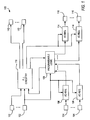
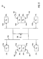
- FIG. 2 shows an embodiment of PLL circuitry.
- PLL circuitry 210 receives an input reference signal via input 218 (unlike PLL circuitry 110, only one input signal is received in this embodiment). That input signal is applied to prescale frequency divider 220.
- Divider 220 divides the frequency of the input reference signal by a factor N, which is preferably a programmable parameter of PLD 100 stored in, for example, a programmable function control element of PLD 100.
- the output of divider 220 is applied as a driving clock signal to one input of phase/frequency detector (PFD) circuitry 222.
- PFD circuitry 222 which can be conventional, also receives the output signal of feedback frequency divider 224.
- PFD circuitry 222 produces an output signal which is indicative of the phase/frequency difference between the two signals applied to it. (A more complete depiction of PFD circuitry 222 is shown in FIG. 3 and described below).
- the output signal of PFD circuitry 222 is applied as a control signal to voltage controlled oscillator (VCO) 226.
- VCO 226 produces k1 output signals (where K1 is an integer), each of which is phase-shifted by preferably an increasing multiple of 360°/k1.
- the output signals of VCO 226 are applied to multiplexer circuitry 228 and feedback multiplexer 230.
- Multiplexer 230 feeds one of the VCO 226 output signals to feedback frequency divider 224.
- the particular VCO 226 output signal fed to divider 224 can be fixed by design, programmed by a user, or rotated or alternated among the VCO 226 output signals by control logic that either is fixed by design or programmed by a user.
- Divider 224 divides the frequency of the signal applied to it by factor M to produce the above-mentioned second (feedback) input to PFD circuitry 222.
- Factor M is preferably a programmable parameter of PLD 100 stored in, for example, a programmable function control element of PLD 100.
- Multiplexer circuitry 228 receives all k1 VCO 226 output signals and programmably selects which of those signals to feed to post-scale frequency-divider circuitry 232.
- Divider circuitry 232 preferably includes multiple counter/frequency-divider circuits, which in the embodiment shown in FIG. 2 is six. Note that the number of individual counter or frequency-divider circuits does not have to equal the number of VCO output signals.
- Multiplexer circuitry 228 is preferably programmable by a user, but may alternatively be fixed to output, for example, each VCO output signal to a respective one of the individual frequency-divider circuits, assuming the number of divider circuits equals the number of VCO output signals.
- Each individual divider circuit divides the frequency of the signal applied to it by its corresponding factor C0 - Cn1 (where n1 is an integer and in FIG. 2 equals five).
- Each of factors C0 - Cn1 is preferably an independently programmable parameter stored in, for example, one or more programmable function control elements of PLD 100.
- each of factors C0 - Cn1 may be different, the same, or combinations thereof.
- the resulting output signals of post-scale frequency-divider circuitry 232 are applied to multiplexers 234, 236, and 238.
- Multiplexers 234, 236, and 238 are each dynamically programmably controlled to output any one of their inputs to any one of their outputs.
- Multiplexer 234 couples selected signals to up to k2 clock I/O pins (CLKOUT; e.g., pins 112 of FIG. 1 ).
- Constant k2 is an integer typically less than or equal to k1. For example, if k1 is equal to eight, k2 may be equal to six.
- Multiplexer 236 couples selected signals to up to k3 global clock (GCLK) networks. Constant k3 is also an integer typically less than or equal to k1.
- k3 may be equal to four.
- multiplexer 238 couples selected signals to up to k4 local clock (LCLK) networks.
- Constant k4 is likewise an integer typically less than or equal to k1.
- k4 may also be equal to eight.
- the eight may be two groups of the same four signals for use in two local regions designed to have the same clocking.
- FIG. 2a shows an embodiment of a dynamically configurable multiplexer that can be used for each of multiplexers 234, 236, and 238.
- Multiplexer 235 includes a group 237 of inputs which are dynamically selectable by a user.
- multiplexer 235 allows any one of a PLL output, clock pin, or core signal, for example, to be selectably driven onto, for example, a global (gclk) or local (lclk) clock network.
- Signals CR_GCLKMUXCTRL and CR_GCLKMUXSEL are programming bits used to either configure multiplexer 235 to be dynamically reconfigurable or fixed (i.e., not dynamically reconfigurable).
- An embodiment of enablement circuitry 239 is shown in FIG. 11 and described further below.
- PLL circuitry 210 provides a high degree of configurability.
- the six modified clock signals produced by circuitry 232 can have different phases and different frequencies, different phases and the same frequencies, the same phase and different frequencies, or combinations thereof.
- each of the six modified clock signals can be programmably routed where needed. None are limited or partitioned to only particular circuits, I/O pins, or uses.
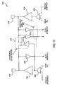
- FIG. 3 shows an embodiment of phase/frequency detector (PFD) circuitry 222.
- PFD circuitry 322 typically includes a phase/frequency detector circuit 323, which receives the input and feedback clock signals.
- Detector circuit 323 produces "up” or “down” output signal pulses depending on whether the phase of the input clock signal leads or lags the phase of the feedback clock signal.
- the width of the "up” or “down” signal pulses is typically controlled by detector circuit 323 to be proportional to the phase difference between the input and feedback clock signals.
- the “up” or “down” signals are fed to charge pump circuit 325, which provides a transfer function of those signals to an output signal voltage at a level between the power supply voltage of PLD 100 and ground.
- the "up” and “down” signals switch an internal current source to deliver a charge to move the charge pump output signal voltage up or down during each clock cycle.
- the output signal of charge pump circuit 325 is applied to low-pass filter circuit 327, which smoothes the signal for application as a control signal to an associated VCO (e.g., VCO 226).
- VCO e.g., VCO 2266.
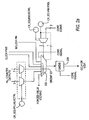
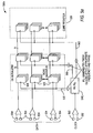
- FIG. 4 shows an embodiment of PLL circuitry in accordance with the invention.
- PLL circuitry 410 includes prescale frequency divider 420, phase/frequency detector (PFD) circuitry 422, voltage controlled oscillator (VCO) 426, multiplexer circuitry 428, feedback multiplexer 430, post-scale frequency-divider circuitry 432, and multiplexers 434, 436, and 438. These elements operate similarly, if not identically, to the corresponding elements of PLL circuitry 210. Note that the number of outputs shown in FIG.
- VCO 426 8 outputs
- these elements may be configured or replaced with other elements to have more or less outputs.
- PLL circuitry 410 advantageously has enhanced input signal selection and synchronization capability.
- PLL circuitry 410 includes multiplexers 440, 442, and 448, synchronizing circuit 446, switchover circuit 450, and AND gate 452.
- Multiplexers 440 and 442 both receive multiple input signals from a number of clock input pins (which in this embodiment is four; note that other numbers of input signals from clock pins may be used). These clock input pins are preferably closely located and available as a matched reference to PLL circuitry 410. Any of these pins may be used for I/O delay compensation and clock network delay compensation. These pins may be used, for example, by memory interfaces, such as for RLDRAM (reduced latency dynamic random access memory).
- RLDRAM reduced latency dynamic random access memory
- Multiplexers 440 and 442 both also receive a core input clock signal, which may be an internal clock signal originating from any clock pin on the chip or it may be generated by another PLL on the chip.
- this input if selected, allows the PLL reference clock signal to come from another PLL on the chip via, e.g., PLL cascading.
- a single reference clock can therefore be used to drive multiple PLLs, rather than having separate clocks (typically requiring respectively separate I/O clock pins) drive respective PLLs. This feature is particularly useful for multiple PCI interfaces, multiple memory interfaces, and those interfaces adhering to known source synchronous protocols where multiple transmit channels using a common reference clock are required.
- FIG. 5 shows an embodiment of a PLD in accordance with the invention in which a core clock signal is used to drive multiple PLL circuitries adhering to a source synchronous protocol.
- PLD 500 includes core clock network S54 and PLL circuitries 510a-h, which are each preferably LVDS PLL circuitries.
- LVDS low voltage differential signaling
- LVDS is a signaling protocol employing very low voltages and differential signaling, which involves the transmission of pairs of signals that propagate in parallel.
- Each signal is usually a logical complement of the other. That is, when one signal is at a high voltage (e.g., a logical 1), the other is at a low voltage (e.g., a logical 0), and vice versa.
- LVDS PLL circuitries 510a-d operate in transmit mode (TX), while LVDS PLL circuitries 510e-h operate in receive mode (RX).
- RX PLL circuitries 510e-h receive external clock signals from clock pins 502 and generate modified clock signals that can be used on-chip, off-chip, or both.
- TX PLL circuitries 510a-d each receive a core clock signal that can enter clock network 554 at node 556. This core clock signal may be driven by any clock pin or by any general purpose or LVDS PLL circuitry output. This core clock signal can advantageously serve as the input reference signal to LVDS PLL circuitries 510a-d, which then generate modified clock signals that can be used on-chip, off-chip or both.
- FIG. 5a further illustrates PLL circuitry operating in receive mode.
- PLL circuitry 510j receives an external clock from clock pins 502. This external clock has its edge in a particular phase relationship with data being received at I/O pins 504.
- PLL circuitry 510j generates several clocks. One is a high speed clock at output 558 used for registers 506, which are closest to the I/O pins.
- a second clock at output 560 is at a lower speed. It is equal to the high speed clock frequency divided by a deserialization factor.
- a common deserialization factor is 8, resulting in a clock frequency 1/8 the frequency of the clock at output 558. This second clock is routed to a second set of registers.
- a third clock at output 562 typically has the same frequency as the second clock and is routed to registers in programmable logic 508. Multiple registers are used for each data channel, and the number of registers preferably equals the deserialization factor.
- PLL circuitry 510j advantageously establishes and maintains the phase relationship and frequency of clocks at outputs 558, 560, and 562 with respect to the external clock. Note that in receive mode, PLL circuitry 510j uses only the reference clock sent with the data. Thus, individual PLL circuitry is used for each interface, because each interface can have a different phase of frequency relationship.
- FIG. 5b further illustrates PLL circuitry operating in transmit mode.
- the source synchronous channel sends out both data (at I/O pins 516) and a TX clock (at clock pins 512).
- PLL circuitry 510k can therefore receive a reference clock from any pin or internally generated core clock because no phase relationship is required between this reference clock and the TX data and clock. If multiple channels are required, a single core clock advantageously can be used to drive multiple TX PLL circuitries, as shown in FIG. 5 .
- multiplexers 440 and 442 are programmable preferably by a user to select two of the multiple input signals to feed to synchronizing circuit 446.
- Synchronizing circuit 446 ensures that the start-up of PLL circuitry 410 occurs in a synchronous manner.
- circuit 446 is intended to prevent glitches on the reference clock signal, which could result in erroneous timing for PLL circuitry 410.
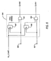
- FIG. 6 shows an embodiment of a synchronizing circuit in accordance with the invention.
- Synchronizing circuit 646 includes latches 647 and 649 and AND gates 651 and 653.
- Latch 647 receives at input 655 the input signal selected by multiplexer 440, while latch 649 receives at input 657 the input signal selected by multiplexer 442.
- a PLL start signal enables the reference clock on the falling edge to ensure that adequate time is allowed before the next rising edge of the clock.
- Corresponding waveforms are shown in FIG. 6a .
- Additional registers could be inserted to delay the enabling of the reference clock to allow portions of the PLL circuitry to be enabled before the two output signals, CLKIN0 and CLKIN1, begin toggling.
- This alternative embodiment is illustrated in FIG. 6b , where the PLL start signal is used to generate a staged start-up sequence that first enables the counters/frequency dividers and then the VCO.
- the two synchronizing circuit outputs are fed to multiplexer 448 and switchover circuit 450.
- Multiplexer 448 is programmable by a user and accordingly outputs one of the two signals selected by the user to serve as the input reference signal.
- the selected input reference signal is fed to AND gate 452, which also receives an input signal from switchover circuit 450.
- switchover circuit 450 allows the selected reference signal to propagate through AND gate 452 to prescale frequency divider 420.
- switchover circuit 450 monitors the two output signals received from synchronizing circuit 446. If the selected clock signal stops running for some reason, switchover circuit 450 will automatically cause the other output signal from synchronizing circuit 446 to be used as the input reference signal. This feature can be used for clock redundancy or for a dual clock domain application.
- switchover circuit 450 can be preferably manually controlled based on a user control signal. This allows a user, for example, to switch between two input reference signals of different frequencies.
- PLL circuitry 410 further has enhanced feedback capability and includes feedback frequency divider 424, spread spectrum counter 458, and multiplexer 460.
- Multiplexer 460 is programmable and receives an output signal from multiplexer 430 and an external feedback signal. By programming multiplexer 460 to output the external feedback signal, an external clock signal can be aligned with the input reference clock signal. This advantageously allows a user to remove clock delay and skew between devices/chips.
- Spread spectrum counter 458 helps prevent corrupted data and intermittent system errors that can be caused by radiated noise from high frequency clock signals.
- PLL circuitries 210 and 410 are both advantageously fully programmable both at power up and during user mode (i.e., dynamically), thus providing a high degree of flexibility.
- Programmable parameters include coarse and fine phase shifting, counter values (i.e., frequency divisors), and duty cycle.
- each counter/frequency divider circuit of frequency-divider circuitries 232 and 432 can be connected to several different output sources including global clock networks, local clock networks, and external clock buffers. By providing these flexible multiplexing regions on the divider circuit outputs, a user can advantageously configure their system in a very flexible manner.
- PLL circuitries 210 and 410 can thus be used to generate multiple internal clock references as well as provide off-chip reference clocks.
- a single frequency divider circuit can be used to generate both an internal reference clock and an external clock reference.
- Other advantages include being able to dynamically switch to any of the multiple input reference signals (in PLL circuitry 410) and to any of the global or local clocks. Allowing a user to dynamically configure PLL circuitry of the invention avoids having to reprogram an entire PLD, which advantageously reduces overall system cost.
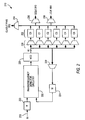
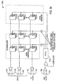
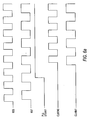
- FIG. 7 shows an example of a clock multiplexer pattern that can be used with PLL circuitries of the invention.
- Pattern 700 includes two general purpose PLL circuitries 710, which may be, for example, either PLL circuitry 210 or 410.
- Each vertical line can be thought of as a single multiplexer with each circle representing a signal that can connect to the multiplexer.
- CLKPIN# represents standard clock pins
- nCLKPIN# represent additional clock pins available when the input clock is not a differential signal.
- the GCKDRV# (global clock driver) and LCKDRV# (local clock driver) signals provide a way for generic logic to drive onto clock networks without having to first drive out via an I/O pin and then back into the clock network via another I/O pin. These multiplexer connections can be used for signals that have a high fanout.
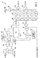
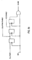
- FIG. 8 shows an example of a multiplexer pattern for external clock outputs that can be used with PLL circuitries of the invention.
- Pattern 800 includes output pins 812 and general purpose PLL circuitry 810, which may be, for example, either PLL circuitry 210 or 410. Any output signal from PLL circuitry 810 can be routed to any output pin 812.
- the extclken# (external clock enable) signals advantageously allow a user to dynamically enable and disable clock pins synchronously. This can be used to implement a system power-down capability to reduce power consumption. Note that the even numbered outputs (i.e., ECK0, ECK2, ...) can be used with their adjacent odd numbered outputs (i.e., ECK1, ECK3, ..) for differential signaling.
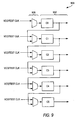
- FIG. 9 shows an alternative arrangement to multiplexer circuitries 228/428 and frequency-divider circuitries 232/432.
- Cascaded PLL output stage 900 advantageously allows PLL circuitries of the invention to programmably divide down signal frequencies by orders of magnitude.
- the output of any of the first n-1 frequency dividers 932 (where n is the total number of frequency dividers) can be programmably selected by the appropriate multiplexer of multiplexer circuitry 928 to be the input of the next frequency divider 932.
- the output of frequency divider C0 can be used as an on-chip local clock and as an input to frequency divider C1.
- the programmable cascading does not need to begin with the output of frequency divider C0, nor does it need to continue to the nth frequency divider (which in this embodiment is divider C5).
- the output of divider C2 can be cascaded to divider C3, whose output can be cascaded to divider C4, while the outputs of dividers C0, C1, and C5 can be used independently.
- the VCO/test clk input to each frequency divider represents the multiple VCO output signals.
- FIG. 10 shows an embodiment of configurable clock buffer circuitry in accordance with the invention.
- clock buffer circuitry 1000 supports generic I/O functionality as well as I/O clock functions and both input and output capability.
- Buffer circuitry 1000 includes multiplexers 1062 and 1064; buffer/drivers 1066, 1068, 1070, 1072, and 1074; and differential buffer 1076.
- Buffer circuitry 1000 is coupled to I/O-clock pins 1078 and can be configured to allow pins 1078 to be driven by PLL circuitry (thus making them clock pins) or to be driven by an I/O interface (thus making them generic I/O pins).
- Buffer circuitry 1000 can further be configured to allow one of pins 1078 to be used as a PLL external feedback pin (thus becoming a delay compensation buffer).
- PLL circuitry can be configured as a zero delay buffer. This is preferable to known methods of using delay cells because only the buffers being compensated out are used in this configuration.
- FIG. 11 shows synchronous PLL enablement circuitry in accordance with the invention.
- Enablement circuitry 1100 includes latch 1182, AND gate 1184, and clock driver 1186.
- Signal ENOUT is a core signal under user control used to dynamically control enabling and disabling of clocks.
- Signal ENOUTCTRL is a programming bit that allows the clock to always be enabled if a user does not use the disable feature.
- NPST is the register preset, which is active low, meaning that a low voltage signal (e.g., a logical 0 signal) at that input causes the output to go high.
- PLCs can be a relatively simple programmable connector such as a switch or a Plurality of switches for connecting any one of several inputs to an output.
- each PLC can be a somewhat more complex element which is capable of performing logic (e.g., by logically combining several of its inputs) as well as making a connection.
- each PLC can be product term logic, implementing functions such as AND, NRND, OR, or NOR. Examples of components suitable for implementing PLCs are EPROMs, EEPROMs, pass transistors, transmission gates, antifuses, laser fuses, metal optional links, etc.
- PLDs having PLL circuitry of the invention are not limited to any one technology, but advantageously can be implemented in various technologies.
- FCEs programmable, function control elements
- FCEs can be implemented in any of several different ways.
- FCEs can be SRAMs, DRAMs, first-in first-out ("FIFO") memories, EPROMs, EEPROMs, function control registers (e.g., as in Wahlstrom U.S. patent 3,473,160 ), ferro-electric memories, fuses, antifuses, or the like.
- the FCEs that control the PLCs and divider circuits of the invention are preferably programmed in the same way and at the same time that programmable logic 108 in FIG. 1 is programmed.
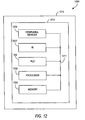
- Data processing system 1200 includes programmable logic device 100, which is an integrated circuit, and may be an integrated circuit chip, that includes PLL circuitry in accordance with the invention.
- PLD 100 may be field programmable, mask programmable, or programmable in any other way. It may be one-time-only programmable, or it may be reprogrammable.
- System 1200 may also include one or more of the following components: a processor 1203; memory 1205; I/O circuitry 1207; and peripheral devices 1209. These components are coupled together by a system bus 1211 and are populated on a circuit board 1213, which is contained in an end-user system 1215. Communication among the various components shown in FIG. 12 , and/or with external circuitry, may be of any known type to any desired extent.
- System 1200 can be used in a wide variety of applications, such as computer networking, data networking, instrumentation, video processing, digital signal processing, or any other application where the advantage of using programmable or reprogrammable logic is desirable.
- PLD 100 can be used to perform a variety of different logic functions.
- PLD 100 can be configured as a processor or controller that works in cooperation with processor 1203.
- PLD 100 may also be used as an arbiter for arbitrating access to a shared resource in system 1200.
- PLD 100 can be configured as an interface between processor 1203 and one of the other components in system 1200. Note that system 1200 is only exemplary and in no way should be construed to limit the true scope of the invention.
Landscapes
- Stabilization Of Oscillater, Synchronisation, Frequency Synthesizers (AREA)
- Logic Circuits (AREA)
Abstract
Description
- This invention relates to programmable logic integrated circuit devices, and more particularly to configurable phase-locked loop (PLL) circuitry for programmable logic devices.
- Programmable logic integrated circuit devices are well known and often include large numbers of programmable logic blocks, memory blocks, and programmable interconnection resources. Logic blocks are programmable by a user to perform various logic functions desired by the user. Memory blocks may be used by the user to store and subsequently output data. Interconnection resources are programmable by the user to make any of a wide range of connections between inputs of the programmable logic device and inputs of the logic and memory blocks, between outputs of the logic and memory blocks and outputs of the device, and between outputs and inputs of the logic and memory blocks. Although each logic block is typically able to perform only a relatively small logic task, such interconnections allow the programmable logic device to perform extremely complex logic functions.
- Providing PLL circuitry on programmable logic devices is also well known. PLL circuitry produces an output signal that is continually adjusted to maintain a constant frequency and phase relationship with an input reference signal (the PLL circuitry thus "locks" onto that frequency and phase relationship). PLL circuitry may be used to counteract clock signal propagation delay on the programmable logic device, convert from one clock signal frequency (e.g., an input clock signal frequency) to another different clock signal frequency (e.g., to be output by the device), and more generally to provide one or more external clock signals, internal global clock signals, or internal local/regional clock signals.
- The configurability of known PLL circuitry, however, is typically limited. For example, the frequency range of output signals produced by known PLL circuitry may be too narrow for many applications in which a programmable logic device could be used. Furthermore, the number and configurability of PLL outputs may be too limited. For example, known PLL circuitry may not have enough outputs available for connection to I/O pins for off-chip clocking applications. Moreover, known PLL circuitry may not have enough outputs available for connection to on-chip global or local clocking networks. Thus, the configurability of known PLL circuitry on programmable logic devices may limit the number of designs that can be implemented on the device and thus the number of applications in which a programmable logic device could otherwise be used.
- In view of the foregoing, it would be desirable to be able to provide highly configurable PLL circuitry in order to increase the number of designs and applications in which programmable logic devices can be used.
-
US2001/0030565 A1 discloses a scheme in which a phase-locked loop circuit produces a multiphase clock whose output signals can be routed, by a selector circuit, to a frequency divider circuit. - The invention is defined in the appended claims, to which reference should now be made.
- Advantageously, PLL circuitry and methods of the invention can be used to implement a wide range of designs including, for example, frequency synthesizers and zero delay buffers. This notably increases the number of designs and applications in which a programmable logic device can be used.
- The above and other advantages of the invention will be apparent upon consideration of the following detailed description, taken in conjunction with the accompanying drawings, in which like reference characters refer to like parts throughout, and in which:
-
FIG. 1 is a simplified block diagram of an illustrative embodiment of representative portions of a programmable logic integrated circuit device according to the invention; -
FIG. 2 is a simplified block diagram of PLL circuitry; -
FIG. 2a is a simplified block diagram of an embodiment of a dynamically configurable multiplexer; -
FIG. 3 is a more detailed, but still simplified block diagram of a typical portion of the PLL circuitry ofFIG. 2 ; -
FIG. 4 is a simplified block diagram of an embodiment of PLL circuitry according to the invention; -
FIGS. 5 ,5a , and5b are simplified block diagrams illustrating programmable logic integrated circuit devices employing PLLs configured in transmit and receive modes according to the invention; -
FIG. 6 is a simplified block diagram of a synchronizing circuit for PLL circuitry according to the invention; -
FIG. 6a is a timing diagram of signals fromFIG. 6 ; -
FIG. 6b is a simplified block diagram of an alternative portion of the synchronizing circuit ofFIG. 6 according to the invention; -
FIG. 7 is a simplified block diagram of a clock multiplexing pattern according to the invention; -
FIG. 8 is a simplified block diagram of an external clock multiplexing pattern according to the invention; -
FIG. 9 is a simplified block diagram of a cascaded portion of PLL circuitry according to the invention; -
FIG. 10 is a simplified block diagram of configurable clock buffer circuitry according to the invention; -
FIG. 11 is a simplified block diagram of PLL enablement circuitry according to the invention; and -
FIG. 12 is a simplified block diagram of an illustrative system employing the invention. -
FIG. 1 shows an illustrative programmable logic integrated circuit device (PLD) 100 in accordance with the invention. PLD 100 has one or more clocksignal input pins 102 for receiving one or more clock signals from circuitry external to the device. PLD 100 also includes a plurality of input/output ("I/O")pins 104 for receiving data and/or control signals from external circuitry. (For convenience herein, all data and control signals other than clock signals will be referred to simply as data signals.) The data signals frompins 104 may be applied to I/O registers 106 for temporary storage and output by those registers. An input clock signal applied to apin 102 may be applied to I/O registers 106 to control the operation (in particular, the timing) of those registers. The data signals output byregisters 106 are applied toprogrammable logic 108 ofPLD 100. (As an alternative to usingregisters 106, data frompins 104 may be applied more directly to logic 108 (i.e., without first being input to registers 106).)Programmable logic 108 may also receive an input clock signal from apin 102 and generally performs at least some operations on the input data frompins 104 and/orregisters 106 at a rate determined by the frequency of a received clock signal. In other words, some or all of the data applied topins 104 may be synchronized with a clock signal received from apin 102, andprogrammable logic 108 may partially process that data in synchronism with that clock signal. - Multiple input clock signals applied to
pins 102 may be applied to phase-locked loop ("PLL")circuitry 110 in accordance with the invention.PLL circuitry 110 may also receive an internal clock signal fromprogrammable logic 108, which may have been generated onPLD 100 and/or derived from another clock signal received from one ofclock pins 102.PLL circuitry 110 programmably selects one of the input clock signals for use as an input reference signal and provides multiple modified clock output signals which have desired frequency relationships to the input reference signal. For example, the frequencies of the modified clock output signals produced byPLL circuitry 110 may be higher and/or lower than the input reference signal frequency. The modified clock signals produced byPLL circuitry 110 advantageously may be programmably applied to any or all of clocksignal output pins 112,programmable logic 108, and I/O registers 114. -
Programmable logic 108 can be configured to perform at least some data processing at one or more rates determined by the one or more modified clock signals produced byPLL circuitry 110. For example,programmable logic 108 may perform some data processing in synchronism with a modified clock signal produced byPLL circuitry 110. Output data signals fromprogrammable logic 108 may be applied to I/O pins 116, possibly via I/O registers 114, which may register those data signals on their way to pins 116 at possibly another modified clock signal rate. Furthermore, PLD 100 may output data viapins 116 at a modified clock signal frequency that may or may not be the same as, and/or in synchronism with, any of the modified clock signals applied tooutput clock pins 112. - Note that in other embodiments of the invention (see, e.g.,
FIG. 10 and its accompanying description below),pins - Although
FIG. 1 may appear to show fixed interconnections among the various circuit elements, note that on a programmable logic device such asPLD 100 there is typically a high degree of programmability and therefore signal routing flexibility in the interconnection resources that are provided. This programmability of interconnection resources, which is well known in the art, is not shown to avoid unnecessarily complicating the FIGS. Thus not all of the interconnections shown inFIG. 1 (or in any of the subsequently described FIGS.) may be present in all uses ofPLD 100, and/or other interconnections not shown inFIG. 1 (or other FIGS.) may be present in some uses ofPLD 100. Those skilled in the art will also appreciate that the circuit elements and interconnection resources shown inFIG. 1 may be only a part of more extensive circuit element and interconnection resources provided onPLD 100. Examples of programmable logic devices in which the invention can be implemented are found in Cliff et al.U.S. Patent No. 5,689,195 ; Cliff et al,U.S. Patent No. 5,909,126 ; and Jefferson et al.U.S. Patent No. 6,215,326 . -
FIG. 2 shows an embodiment of PLL circuitry.PLL circuitry 210 receives an input reference signal via input 218 (unlikePLL circuitry 110, only one input signal is received in this embodiment). That input signal is applied toprescale frequency divider 220.Divider 220 divides the frequency of the input reference signal by a factor N, which is preferably a programmable parameter ofPLD 100 stored in, for example, a programmable function control element ofPLD 100. The output ofdivider 220 is applied as a driving clock signal to one input of phase/frequency detector (PFD)circuitry 222.PFD circuitry 222, which can be conventional, also receives the output signal offeedback frequency divider 224.PFD circuitry 222 produces an output signal which is indicative of the phase/frequency difference between the two signals applied to it. (A more complete depiction ofPFD circuitry 222 is shown inFIG. 3 and described below). The output signal ofPFD circuitry 222 is applied as a control signal to voltage controlled oscillator (VCO) 226.VCO 226 produces k1 output signals (where K1 is an integer), each of which is phase-shifted by preferably an increasing multiple of 360°/k1. In one embodiment, for example,VCO 226 may output six signals (i.e., k1 = 6), wherein the output signals are each preferably phase-shifted with respect to the input reference signal at 60° intervals (e.g., 60°, 120°, 180°, 240°, 300°, and 360°). In another embodiment, for example, eight signals may be output (resulting in 45° phase shift increments). The output signals ofVCO 226 are applied tomultiplexer circuitry 228 andfeedback multiplexer 230. -
Multiplexer 230 feeds one of theVCO 226 output signals tofeedback frequency divider 224. Theparticular VCO 226 output signal fed todivider 224 can be fixed by design, programmed by a user, or rotated or alternated among theVCO 226 output signals by control logic that either is fixed by design or programmed by a user.Divider 224 divides the frequency of the signal applied to it by factor M to produce the above-mentioned second (feedback) input toPFD circuitry 222. Factor M is preferably a programmable parameter ofPLD 100 stored in, for example, a programmable function control element ofPLD 100. -
Multiplexer circuitry 228 receives allk1 VCO 226 output signals and programmably selects which of those signals to feed to post-scale frequency-divider circuitry 232.Divider circuitry 232 preferably includes multiple counter/frequency-divider circuits, which in the embodiment shown inFIG. 2 is six. Note that the number of individual counter or frequency-divider circuits does not have to equal the number of VCO output signals.Multiplexer circuitry 228 is preferably programmable by a user, but may alternatively be fixed to output, for example, each VCO output signal to a respective one of the individual frequency-divider circuits, assuming the number of divider circuits equals the number of VCO output signals. Each individual divider circuit divides the frequency of the signal applied to it by its corresponding factor C0 - Cn1 (where n1 is an integer and inFIG. 2 equals five). Each of factors C0 - Cn1 is preferably an independently programmable parameter stored in, for example, one or more programmable function control elements ofPLD 100. Thus, each of factors C0 - Cn1 may be different, the same, or combinations thereof. - The resulting output signals of post-scale frequency-
divider circuitry 232 are applied tomultiplexers Multiplexers Multiplexer 234 couples selected signals to up to k2 clock I/O pins (CLKOUT; e.g., pins 112 ofFIG. 1 ). Constant k2 is an integer typically less than or equal to k1. For example, if k1 is equal to eight, k2 may be equal to six.Multiplexer 236 couples selected signals to up to k3 global clock (GCLK) networks. Constant k3 is also an integer typically less than or equal to k1. Thus, for example, if k1 is equal to eight, k3 may be equal to four. Lastly, multiplexer 238 couples selected signals to up to k4 local clock (LCLK) networks. Constant k4 is likewise an integer typically less than or equal to k1. For example, if k1 is equal to eight, k4 may also be equal to eight. Moreover, the eight may be two groups of the same four signals for use in two local regions designed to have the same clocking. -
FIG. 2a shows an embodiment of a dynamically configurable multiplexer that can be used for each ofmultiplexers Multiplexer 235 includes agroup 237 of inputs which are dynamically selectable by a user. Advantageously,multiplexer 235 allows any one of a PLL output, clock pin, or core signal, for example, to be selectably driven onto, for example, a global (gclk) or local (lclk) clock network. Signals CR_GCLKMUXCTRL and CR_GCLKMUXSEL are programming bits used to either configuremultiplexer 235 to be dynamically reconfigurable or fixed (i.e., not dynamically reconfigurable). An embodiment ofenablement circuitry 239 is shown inFIG. 11 and described further below. - Advantageously,
PLL circuitry 210 provides a high degree of configurability. For example, by appropriately programmingmultiplexer circuitry 228 anddivider circuitry 232, the six modified clock signals produced bycircuitry 232 can have different phases and different frequencies, different phases and the same frequencies, the same phase and different frequencies, or combinations thereof. Moreover, each of the six modified clock signals can be programmably routed where needed. None are limited or partitioned to only particular circuits, I/O pins, or uses. -
FIG. 3 shows an embodiment of phase/frequency detector (PFD)circuitry 222.PFD circuitry 322 typically includes a phase/frequency detector circuit 323, which receives the input and feedback clock signals.Detector circuit 323 produces "up" or "down" output signal pulses depending on whether the phase of the input clock signal leads or lags the phase of the feedback clock signal. The width of the "up" or "down" signal pulses is typically controlled bydetector circuit 323 to be proportional to the phase difference between the input and feedback clock signals. The "up" or "down" signals are fed to chargepump circuit 325, which provides a transfer function of those signals to an output signal voltage at a level between the power supply voltage ofPLD 100 and ground. The "up" and "down" signals switch an internal current source to deliver a charge to move the charge pump output signal voltage up or down during each clock cycle. The output signal ofcharge pump circuit 325 is applied to low-pass filter circuit 327, which smoothes the signal for application as a control signal to an associated VCO (e.g., VCO 226). In sum, when the phase of the input clock signal leads the phase of the feedback clock signal, an "up" signal is generated bydetector circuit 323. This results in an increase in the frequency of the feedback clock signal. Conversely, when the phase of the input clock signal lags the phase of the feedback clock signal,detector circuit 323 produces a "down" signal, which causes a decrease in the frequency of the feedback clock signal. -
FIG. 4 shows an embodiment of PLL circuitry in accordance with the invention.PLL circuitry 410 includesprescale frequency divider 420, phase/frequency detector (PFD)circuitry 422, voltage controlled oscillator (VCO) 426,multiplexer circuitry 428,feedback multiplexer 430, post-scale frequency-divider circuitry 432, andmultiplexers PLL circuitry 210. Note that the number of outputs shown inFIG. 4 for VCO 426 (8 outputs), multiplexer circuitry 428 (6 outputs), multiplexer 434 (6 outputs), multiplexer 436 (4 outputs), and multiplexer 438 (8 outputs) are merely illustrative and that these elements may be configured or replaced with other elements to have more or less outputs. -
PLL circuitry 410 advantageously has enhanced input signal selection and synchronization capability.PLL circuitry 410 includesmultiplexers circuit 446,switchover circuit 450, and ANDgate 452.Multiplexers PLL circuitry 410. Any of these pins may be used for I/O delay compensation and clock network delay compensation. These pins may be used, for example, by memory interfaces, such as for RLDRAM (reduced latency dynamic random access memory). -
Multiplexers -
FIG. 5 shows an embodiment of a PLD in accordance with the invention in which a core clock signal is used to drive multiple PLL circuitries adhering to a source synchronous protocol.PLD 500 includes core clock network S54 andPLL circuitries 510a-h, which are each preferably LVDS PLL circuitries. LVDS (low voltage differential signaling) is a signaling protocol employing very low voltages and differential signaling, which involves the transmission of pairs of signals that propagate in parallel. Each signal is usually a logical complement of the other. That is, when one signal is at a high voltage (e.g., a logical 1), the other is at a low voltage (e.g., a logical 0), and vice versa.LVDS PLL circuitries 510a-d operate in transmit mode (TX), whileLVDS PLL circuitries 510e-h operate in receive mode (RX). (Note thatPLL circuitries 510a-h can each operate in either or both modes in accordance with the invention).RX PLL circuitries 510e-h receive external clock signals from clock pins 502 and generate modified clock signals that can be used on-chip, off-chip, or both.TX PLL circuitries 510a-d each receive a core clock signal that can enterclock network 554 atnode 556. This core clock signal may be driven by any clock pin or by any general purpose or LVDS PLL circuitry output. This core clock signal can advantageously serve as the input reference signal toLVDS PLL circuitries 510a-d, which then generate modified clock signals that can be used on-chip, off-chip or both. -
FIG. 5a further illustrates PLL circuitry operating in receive mode.PLL circuitry 510j receives an external clock from clock pins 502. This external clock has its edge in a particular phase relationship with data being received at I/O pins 504.PLL circuitry 510j generates several clocks. One is a high speed clock atoutput 558 used forregisters 506, which are closest to the I/O pins. A second clock atoutput 560 is at a lower speed. It is equal to the high speed clock frequency divided by a deserialization factor. A common deserialization factor is 8, resulting in aclock frequency 1/8 the frequency of the clock atoutput 558. This second clock is routed to a second set of registers. A third clock atoutput 562 typically has the same frequency as the second clock and is routed to registers inprogrammable logic 508. Multiple registers are used for each data channel, and the number of registers preferably equals the deserialization factor.PLL circuitry 510j advantageously establishes and maintains the phase relationship and frequency of clocks atoutputs PLL circuitry 510j uses only the reference clock sent with the data. Thus, individual PLL circuitry is used for each interface, because each interface can have a different phase of frequency relationship. -
FIG. 5b further illustrates PLL circuitry operating in transmit mode. In transmit mode, the source synchronous channel sends out both data (at I/O pins 516) and a TX clock (at clock pins 512).PLL circuitry 510k can therefore receive a reference clock from any pin or internally generated core clock because no phase relationship is required between this reference clock and the TX data and clock. If multiple channels are required, a single core clock advantageously can be used to drive multiple TX PLL circuitries, as shown inFIG. 5 . - Returning to
FIG. 4 ,multiplexers circuit 446. Synchronizingcircuit 446 ensures that the start-up ofPLL circuitry 410 occurs in a synchronous manner. In particular,circuit 446 is intended to prevent glitches on the reference clock signal, which could result in erroneous timing forPLL circuitry 410. -
FIG. 6 shows an embodiment of a synchronizing circuit in accordance with the invention. Synchronizingcircuit 646 includeslatches gates Latch 647 receives atinput 655 the input signal selected bymultiplexer 440, whilelatch 649 receives atinput 657 the input signal selected bymultiplexer 442. A PLL start signal enables the reference clock on the falling edge to ensure that adequate time is allowed before the next rising edge of the clock. Corresponding waveforms are shown inFIG. 6a . - Additional registers could be inserted to delay the enabling of the reference clock to allow portions of the PLL circuitry to be enabled before the two output signals, CLKIN0 and CLKIN1, begin toggling. This alternative embodiment is illustrated in
FIG. 6b , where the PLL start signal is used to generate a staged start-up sequence that first enables the counters/frequency dividers and then the VCO. - Returning to
FIG. 4 , the two synchronizing circuit outputs are fed to multiplexer 448 andswitchover circuit 450.Multiplexer 448 is programmable by a user and accordingly outputs one of the two signals selected by the user to serve as the input reference signal. The selected input reference signal is fed to ANDgate 452, which also receives an input signal fromswitchover circuit 450. In normal operating mode,switchover circuit 450 allows the selected reference signal to propagate through ANDgate 452 toprescale frequency divider 420.switchover circuit 450 monitors the two output signals received from synchronizingcircuit 446. If the selected clock signal stops running for some reason,switchover circuit 450 will automatically cause the other output signal from synchronizingcircuit 446 to be used as the input reference signal. This feature can be used for clock redundancy or for a dual clock domain application. Moreover,switchover circuit 450 can be preferably manually controlled based on a user control signal. This allows a user, for example, to switch between two input reference signals of different frequencies. -
PLL circuitry 410 further has enhanced feedback capability and includesfeedback frequency divider 424, spreadspectrum counter 458, andmultiplexer 460.Multiplexer 460 is programmable and receives an output signal frommultiplexer 430 and an external feedback signal. Byprogramming multiplexer 460 to output the external feedback signal, an external clock signal can be aligned with the input reference clock signal. This advantageously allows a user to remove clock delay and skew between devices/chips. Spreadspectrum counter 458 helps prevent corrupted data and intermittent system errors that can be caused by radiated noise from high frequency clock signals. Spreadspectrum counter 458, which is coupled tofrequency dividers -
PLL circuitries divider circuitries PLL circuitries -
FIG. 7 shows an example of a clock multiplexer pattern that can be used with PLL circuitries of the invention.Pattern 700 includes two generalpurpose PLL circuitries 710, which may be, for example, eitherPLL circuitry -
FIG. 8 shows an example of a multiplexer pattern for external clock outputs that can be used with PLL circuitries of the invention.Pattern 800 includes output pins 812 and generalpurpose PLL circuitry 810, which may be, for example, eitherPLL circuitry PLL circuitry 810 can be routed to anyoutput pin 812. The extclken# (external clock enable) signals advantageously allow a user to dynamically enable and disable clock pins synchronously. This can be used to implement a system power-down capability to reduce power consumption. Note that the even numbered outputs (i.e., ECK0, ECK2, ...) can be used with their adjacent odd numbered outputs (i.e., ECK1, ECK3, ..) for differential signaling. -
FIG. 9 shows an alternative arrangement to multiplexercircuitries 228/428 and frequency-divider circuitries 232/432. CascadedPLL output stage 900 advantageously allows PLL circuitries of the invention to programmably divide down signal frequencies by orders of magnitude. The output of any of the first n-1 frequency dividers 932 (where n is the total number of frequency dividers) can be programmably selected by the appropriate multiplexer ofmultiplexer circuitry 928 to be the input of thenext frequency divider 932. Thus, for example, the output of frequency divider C0 can be used as an on-chip local clock and as an input to frequency divider C1. Moreover, the programmable cascading does not need to begin with the output of frequency divider C0, nor does it need to continue to the nth frequency divider (which in this embodiment is divider C5). For example, the output of divider C2 can be cascaded to divider C3, whose output can be cascaded to divider C4, while the outputs of dividers C0, C1, and C5 can be used independently. Note that the VCO/test clk input to each frequency divider represents the multiple VCO output signals. -
FIG. 10 shows an embodiment of configurable clock buffer circuitry in accordance with the invention. Advantageously,clock buffer circuitry 1000 supports generic I/O functionality as well as I/O clock functions and both input and output capability.Buffer circuitry 1000 includesmultiplexers drivers differential buffer 1076.Buffer circuitry 1000 is coupled to I/O-clock pins 1078 and can be configured to allowpins 1078 to be driven by PLL circuitry (thus making them clock pins) or to be driven by an I/O interface (thus making them generic I/O pins).Buffer circuitry 1000 can further be configured to allow one ofpins 1078 to be used as a PLL external feedback pin (thus becoming a delay compensation buffer). Whenbuffer circuitry 1000 is configured bidirectionally (allowing both input and output), PLL circuitry can be configured as a zero delay buffer. This is preferable to known methods of using delay cells because only the buffers being compensated out are used in this configuration. - Preferably, all clock sources (global clock, local clocks, and external clocks) associated with PLDs of the invention can be synchronously enabled and disabled. This allows users to dynamically shut down and turn on various portions of their design for power management.
FIG. 11 shows synchronous PLL enablement circuitry in accordance with the invention.Enablement circuitry 1100 includeslatch 1182, ANDgate 1184, andclock driver 1186. Signal ENOUT is a core signal under user control used to dynamically control enabling and disabling of clocks. Signal ENOUTCTRL is a programming bit that allows the clock to always be enabled if a user does not use the disable feature. NPST is the register preset, which is active low, meaning that a low voltage signal (e.g., a logical 0 signal) at that input causes the output to go high. - Note that while multiplexers have been shown throughout the FIGS., they may be alternatively replaced with other types of programmable logic connectors (PLCs). For example, PLCs can be a relatively simple programmable connector such as a switch or a Plurality of switches for connecting any one of several inputs to an output. Alternatively, each PLC can be a somewhat more complex element which is capable of performing logic (e.g., by logically combining several of its inputs) as well as making a connection. In the latter case, for example, each PLC can be product term logic, implementing functions such as AND, NRND, OR, or NOR. Examples of components suitable for implementing PLCs are EPROMs, EEPROMs, pass transistors, transmission gates, antifuses, laser fuses, metal optional links, etc.
- Further note that PLDs having PLL circuitry of the invention are not limited to any one technology, but advantageously can be implemented in various technologies.
- As mentioned above, PLCs (e.g., multiplexers) and divider circuits of the invention are programmable, and their programmable parameters may be stored in various types of programmable, function control elements ("FCEs") (although with certain implementations (e.g., fuses and metal optional links) separate FCTs devices are not required.) FCEs can be implemented in any of several different ways. For example, FCEs can be SRAMs, DRAMs, first-in first-out ("FIFO") memories, EPROMs, EEPROMs, function control registers (e.g., as in Wahlstrom
U.S. patent 3,473,160 ), ferro-electric memories, fuses, antifuses, or the like. The FCEs that control the PLCs and divider circuits of the invention are preferably programmed in the same way and at the same time thatprogrammable logic 108 inFIG. 1 is programmed. - Although the circuitry of the invention has many possible applications, one illustrative use is shown in
FIG. 12 .Data processing system 1200 includesprogrammable logic device 100, which is an integrated circuit, and may be an integrated circuit chip, that includes PLL circuitry in accordance with the invention.PLD 100 may be field programmable, mask programmable, or programmable in any other way. It may be one-time-only programmable, or it may be reprogrammable.System 1200 may also include one or more of the following components: aprocessor 1203;memory 1205; I/O circuitry 1207; andperipheral devices 1209. These components are coupled together by asystem bus 1211 and are populated on acircuit board 1213, which is contained in an end-user system 1215. Communication among the various components shown inFIG. 12 , and/or with external circuitry, may be of any known type to any desired extent. -
System 1200 can be used in a wide variety of applications, such as computer networking, data networking, instrumentation, video processing, digital signal processing, or any other application where the advantage of using programmable or reprogrammable logic is desirable.PLD 100 can be used to perform a variety of different logic functions. For example,PLD 100 can be configured as a processor or controller that works in cooperation withprocessor 1203.PLD 100 may also be used as an arbiter for arbitrating access to a shared resource insystem 1200. In yet another example,PLD 100 can be configured as an interface betweenprocessor 1203 and one of the other components insystem 1200. Note thatsystem 1200 is only exemplary and in no way should be construed to limit the true scope of the invention. - Thus it is seen that highly configurable PLL circuitry outputting multiple signals having programmable phases and frequencies for programmable use as external or internal clocks is provided. One skilled in the art will appreciate that the invention can be practiced by other than the described embodiments, which are presented for purposes of illustration and not of limitation, and the invention is limited only by the claims which follow.
Claims (20)
- A method for concurrently generating a plurality of clock signals in a programmable logic integrated circuit chip, said plurality of clock signals being derived from a reference signal, said method comprising:receiving a plurality of input signals (446);synchronizing said plurality of input signals with an enable signal (646);selecting one of said plurality of input signals as said reference signal (448);producing from said reference signal a plurality of signals having a common frequency and each having a different phase using a phase-locked loop;dividing said common frequency of each of said produced signals concurrently in accordance with programmable selections of frequency divisors (232) to produce output signals each having a frequency and phase; andmultiplexing (234) said output signals in accordance with programmable selections to generate said plurality of clock signals each usable as an off-chip clock signal, an on-chip clock signal, or both.
- The method of claim 1 wherein said frequency of each of said output signals (232) is different than or the same as one or more of the other of said output signals.
- The method of claim 1 wherein said multiplexing comprises programmably coupling (228) one of said output signals to an output pin (502) of said integrated circuit chip for use as an off-chip clock signal.
- The method of claim 1 wherein said multiplexing comprises programmably coupling (228) one of said output signals to a global clock network (235, 237, 239) for use as an on-chip global clock signal (235, 237, 239), said global clock network being on said integrated circuit chip.
- The method of claim 1 wherein said multiplexing comprises programmably coupling (228) one of said output signals to a clock network for use as an on-chip local clock signal, said clock network being coupled to only a portion of circuits on said integrated circuit chip.
- The method of claim 1 wherein said receiving comprises:generating one of said plurality of input signals on said integrated circuit chip (1200); andreceiving from another integrated circuit chip via an input pin another one of said plurality of input signals.
- A programmable logic integrated circuit chip (100) operative to output a plurality of clock signals having programmable phases and frequencies, said clock signals each usable as an off-chip clock signal, an on-chip clock signal, or both;
said circuit comprising:first frequency-divider circuitry (220) operative to receive an input signal (218);phase/frequency detector circuitry (222) coupled to receive output of said first frequency divider circuitry and wherein said phase/frequency detector circuitry comprises a second input;a voltage-controlled oscillator (VCO) (226) coupled to receive output of said phase/frequency detector circuitry (222) and operative to output a plurality of VCO output signals each having a different phase;feedback frequency-divider circuitry (224) coupled to receive one of said plurality of VCO output signals and operative to output a frequency-divided signal to said second input of said phase/frequency detector circuitry (222);first multiplexing circuitry (228) coupled to receive said plurality of VCO output signals and operative to output a plurality of signals selected from said plurality of VCO output signals;a plurality of frequency dividers (232) each coupled to said first multiplexing circuitry to receive one of said plurality of output signals from said first multiplexing circuitry and operative to output a frequency-divided signal; andsecond multiplexing circuitry (234, 236, 238) coupled to receive each of said frequency-divided signals from said plurality of frequency dividers, said second multiplexing circuitry operative to programmably output each received frequency-divided signal to any one of a plurality of signal conductors coupled to said second multiplexing circuitrywherein the programmable logic integrated circuit chip (100) is characterised by further comprising a third multiplexing circuitry coupled to receive a plurality of input signals, said third multiplexing circuitry comprising a synchronization circuit (646) coupled to receive an enable signal and a selectable two (655, 657) of said plurality of input signals, said synchronization circuit comprising two latches (647, 649) clocked by said enable signal, each latch coupled to receive a respective one of said selectable two signals and operative to output a synchronized signal. - The programmable logic integrated circuit chip of claim 7 wherein said plurality of signal conductors are coupled to clock output pins on an integrated circuit chip, a global clock network on said integrated circuit chip, and at least one local clock network coupled to only a portion of the circuits on said integrated circuit ship.
- The programmable logic integrated circuit chip of claim 7, wherein said third multiplexing circuitry is operative to programmably output one of said plurality of input signals to said first frequency-divider circuitry (220).
- The programmable logic integrated circuit chip of claim 7 further comprising switchover circuitry coupled to receive said two synchronized signals from said two latches and operative to automatically output the other of said two synchronized signals should one of said two synchronized signals not be received.
- The programmable logic integrated circuit chip of claim 7 wherein said feedback frequency-divider circuitry comprises a multiplexer and a programmable frequency-divider circuit, said multiplexer coupled to receive said plurality of VCO output signals and operative to output one of said VCO output signals to said programmable frequency-divider circuit, said programmable frequency-divider circuit operative to output a frequency-divided signal to said second input of said phase/frequency detector circuitry.
- The programmable logic integrated circuit chip of claim 7 wherein said circuit is a low voltage differential signaling (LVDS) phase-locked loop circuit.
- The programmable logic integrated circuit chip of claim 7 wherein said circuit is a general purpose phase-locked loop circuit.
- An integrated circuit chip comprising the programmable logic integrated circuit chip of claim 7.
- A programmable logic device comprising the programmable logic integrated circuit chip of claim 7.
- A printed circuit board comprising the programmable logic integrated circuit chip of claim 7 mounted on said printed circuit board.
- The printed circuit board of claim 16 further comprising a memory mounted on said printed circuit board.
- The printed circuit board of claim 16 further comprising processing circuitry mounted on said printed circuit board.
- A system comprising:a processor;a memory coupled to said processor; andthe programmable logic integrated circuit chip of claim 7 coupled to at least one of said processor and said memory.
- A digital processing system comprising:a processor;a memory;a programmable logic device comprising the programmable logic integrated circuit chip of claim 7;input/output circuitry; anda system bus coupling said processor, said memory, said programmable logic device, and said input/output circuitry.
Applications Claiming Priority (2)
| Application Number | Priority Date | Filing Date | Title |
|---|---|---|---|
| US797836 | 2004-03-09 | ||
| US10/797,836 US7098707B2 (en) | 2004-03-09 | 2004-03-09 | Highly configurable PLL architecture for programmable logic |
Publications (2)
| Publication Number | Publication Date |
|---|---|
| EP1575170A1 EP1575170A1 (en) | 2005-09-14 |
| EP1575170B1 true EP1575170B1 (en) | 2012-04-18 |
Family
ID=34827644
Family Applications (1)
| Application Number | Title | Priority Date | Filing Date |
|---|---|---|---|
| EP05251420A Expired - Lifetime EP1575170B1 (en) | 2004-03-09 | 2005-03-09 | Highly configurable pll architecture for programmable logic device |
Country Status (5)
| Country | Link |
|---|---|
| US (2) | US7098707B2 (en) |
| EP (1) | EP1575170B1 (en) |
| JP (1) | JP2005269635A (en) |
| CN (2) | CN1667957B (en) |
| AT (1) | ATE554530T1 (en) |
Families Citing this family (78)
| Publication number | Priority date | Publication date | Assignee | Title |
|---|---|---|---|---|
| US7242229B1 (en) | 2001-05-06 | 2007-07-10 | Altera Corporation | Phase locked loop (PLL) and delay locked loop (DLL) counter and delay element programming in user mode |
| US7200769B1 (en) | 2001-08-29 | 2007-04-03 | Altera Corporation | Self-compensating delay chain for multiple-date-rate interfaces |
| US7167025B1 (en) | 2004-02-14 | 2007-01-23 | Herman Schmit | Non-sequentially configurable IC |
| US7425841B2 (en) | 2004-02-14 | 2008-09-16 | Tabula Inc. | Configurable circuits, IC's, and systems |
| US20050186920A1 (en) * | 2004-02-19 | 2005-08-25 | Texas Instruments Incorporated | Apparatus for and method of noise suppression and dithering to improve resolution quality in a digital RF processor |
| US7234069B1 (en) | 2004-03-12 | 2007-06-19 | Altera Corporation | Precise phase shifting using a DLL controlled, multi-stage delay chain |
| US7126399B1 (en) | 2004-05-27 | 2006-10-24 | Altera Corporation | Memory interface phase-shift circuitry to support multiple frequency ranges |
| US7276933B1 (en) | 2004-11-08 | 2007-10-02 | Tabula, Inc. | Reconfigurable IC that has sections running at different looperness |
| US7317331B2 (en) | 2004-11-08 | 2008-01-08 | Tabula, Inc. | Reconfigurable IC that has sections running at different reconfiguration rates |
| US7330050B2 (en) | 2004-11-08 | 2008-02-12 | Tabula, Inc. | Storage elements for a configurable IC and method and apparatus for accessing data stored in the storage elements |
| US7224181B1 (en) * | 2004-11-08 | 2007-05-29 | Herman Schmit | Clock distribution in a configurable IC |
| US7268586B1 (en) | 2004-11-08 | 2007-09-11 | Tabula, Inc. | Method and apparatus for accessing stored data in a reconfigurable IC |
| US7342415B2 (en) | 2004-11-08 | 2008-03-11 | Tabula, Inc. | Configurable IC with interconnect circuits that also perform storage operations |
| US20060109940A1 (en) * | 2004-11-22 | 2006-05-25 | Troy Beukema | Timing bias compensation for a data receiver with decision-feedback equalizer |
| US7236009B1 (en) | 2004-12-01 | 2007-06-26 | Andre Rohe | Operational time extension |
| US7199607B2 (en) * | 2004-12-22 | 2007-04-03 | Infineon Technologies Ag | Pin multiplexing |
| US7826579B2 (en) * | 2005-02-11 | 2010-11-02 | International Business Machines Corporation | Method and apparatus for generating synchronization signals for synchronizing multiple chips in a system |
| US7230869B1 (en) | 2005-03-15 | 2007-06-12 | Jason Redgrave | Method and apparatus for accessing contents of memory cells |
| US7826519B1 (en) * | 2005-05-23 | 2010-11-02 | Marvell International, Ltd | Method and apparatus for providing coherent phase noise in transceivers or similar systems |
| TWI300653B (en) * | 2005-06-22 | 2008-09-01 | Ind Tech Res Inst | Clock generator and phase locked loop and clock generation method using the same |
| US7414429B1 (en) | 2005-07-19 | 2008-08-19 | Altera Corporation | Integration of high-speed serial interface circuitry into programmable logic device architectures |
| US7304498B2 (en) * | 2005-07-20 | 2007-12-04 | Altera Corporation | Clock circuitry for programmable logic devices |
| US8189729B2 (en) * | 2005-08-03 | 2012-05-29 | Altera Corporation | Wide range and dynamically reconfigurable clock data recovery architecture |
| US7812659B1 (en) | 2005-08-03 | 2010-10-12 | Altera Corporation | Clock signal circuitry for multi-channel data signaling |
| CN1953332B (en) * | 2005-10-17 | 2011-01-12 | 联芯科技有限公司 | Clock generator and communication terminal using the same |
| US7372297B1 (en) | 2005-11-07 | 2008-05-13 | Tabula Inc. | Hybrid interconnect/logic circuits enabling efficient replication of a function in several sub-cycles to save logic and routing resources |
| US7679401B1 (en) | 2005-12-01 | 2010-03-16 | Tabula, Inc. | User registers implemented with routing circuits in a configurable IC |
| US7489162B1 (en) | 2005-12-01 | 2009-02-10 | Tabula, Inc. | Users registers in a reconfigurable IC |
| US7461362B1 (en) | 2005-12-01 | 2008-12-02 | Tabula, Inc. | Replacing circuit design elements with their equivalents |
| US7539278B2 (en) * | 2005-12-02 | 2009-05-26 | Altera Corporation | Programmable transceivers that are able to operate over wide frequency ranges |
| GB2435725A (en) * | 2006-03-03 | 2007-09-05 | Toumaz Technology Ltd | Frequency generation circuit |
| US7529992B1 (en) | 2006-03-27 | 2009-05-05 | Tabula, Inc. | Configurable integrated circuit with error correcting circuitry |
| US7669097B1 (en) | 2006-03-27 | 2010-02-23 | Tabula, Inc. | Configurable IC with error detection and correction circuitry |
| TW200805373A (en) * | 2006-05-19 | 2008-01-16 | Samsung Electronics Co Ltd | A multi-port semiconductor device and method thereof |
| JP4807222B2 (en) * | 2006-10-27 | 2011-11-02 | パナソニック株式会社 | LVDS receiving method and receiving apparatus |
| JP2008147499A (en) * | 2006-12-12 | 2008-06-26 | Fujitsu Ltd | Printed board |
| US7495517B1 (en) | 2006-12-14 | 2009-02-24 | Altera Corporation | Techniques for dynamically adjusting the frequency range of phase-locked loops |
| US7619451B1 (en) * | 2007-02-03 | 2009-11-17 | Altera Corporation | Techniques for compensating delays in clock signals on integrated circuits |
| EP2597777A3 (en) | 2007-03-20 | 2014-08-20 | Tabula, Inc. | Configurable IC having a routing fabric with storage elements |
| US7610566B1 (en) | 2007-03-22 | 2009-10-27 | Tabula, Inc. | Method and apparatus for function decomposition |
| US7814301B2 (en) * | 2007-04-11 | 2010-10-12 | Hewlett-Packard Development Company, L.P. | Clock architecture for multi-processor systems |
| US7532029B1 (en) | 2007-04-18 | 2009-05-12 | Altera Corporation | Techniques for reconfiguring programmable circuit blocks |
| US7821312B1 (en) | 2007-04-18 | 2010-10-26 | Altera Corporation | Techniques for selecting phases of clock signals |
| US7825685B2 (en) | 2007-09-06 | 2010-11-02 | Tabula, Inc. | Configuration context switcher with a clocked storage element |
| US7940132B2 (en) * | 2007-09-27 | 2011-05-10 | Freescale Semiconductor, Inc. | Clock system and applications thereof |
| US8863067B1 (en) | 2008-02-06 | 2014-10-14 | Tabula, Inc. | Sequential delay analysis by placement engines |
| US8130044B2 (en) * | 2008-06-19 | 2012-03-06 | Altera Corporation | Phase-locked loop circuitry with multiple voltage-controlled oscillators |
| US8166435B2 (en) | 2008-06-26 | 2012-04-24 | Tabula, Inc. | Timing operations in an IC with configurable circuits |
| US7928782B2 (en) * | 2009-01-28 | 2011-04-19 | Micron Technology, Inc. | Digital locked loops and methods with configurable operating parameters |
| US8228102B1 (en) * | 2010-03-03 | 2012-07-24 | Altera Corporation | Phase-locked loop architecture and clock distribution system |
| US8406258B1 (en) * | 2010-04-01 | 2013-03-26 | Altera Corporation | Apparatus and methods for low-jitter transceiver clocking |
| US8996906B1 (en) | 2010-05-13 | 2015-03-31 | Tabula, Inc. | Clock management block |
| US8279761B2 (en) * | 2010-05-28 | 2012-10-02 | Altera Corporation | Input/output interface for periodic signals |
| US8686776B2 (en) * | 2012-07-24 | 2014-04-01 | International Business Machines Corporation | Phase rotator based on voltage referencing |
| US9590638B2 (en) | 2012-09-07 | 2017-03-07 | University Of Virginia Patent Foundation | Low power clock source |
| CN103077694B (en) * | 2012-12-20 | 2014-12-24 | 广州视源电子科技股份有限公司 | System and method for removing spread spectrum of LVDS (Low Voltage differential Signaling) |
| US9000801B1 (en) | 2013-02-27 | 2015-04-07 | Tabula, Inc. | Implementation of related clocks |
| WO2014209365A1 (en) | 2013-06-28 | 2014-12-31 | Intel Corporation | Clock generation system with dynamic distribution bypass mode |
| US9225322B2 (en) | 2013-12-17 | 2015-12-29 | Micron Technology, Inc. | Apparatuses and methods for providing clock signals |
| US9413364B2 (en) * | 2014-07-09 | 2016-08-09 | Intel Corporation | Apparatus and method for clock synchronization for inter-die synchronized data transfer |
| US9819345B2 (en) * | 2014-10-02 | 2017-11-14 | Altera Corporation | Scalable 2.5D interface architecture |
| US20160105274A1 (en) * | 2014-10-14 | 2016-04-14 | Gain Ics Llc | Wireless network throughput system and method |
| CN104518789A (en) * | 2014-12-30 | 2015-04-15 | 西安奇维科技股份有限公司 | Method for high-precision digital frequency pulse output |
| CN106294224B (en) * | 2015-05-13 | 2019-10-25 | 瑞昱半导体股份有限公司 | Storage system and its memory entities interface circuit |
| CN106356021B (en) * | 2015-07-14 | 2020-02-14 | 西安诺瓦星云科技股份有限公司 | Method for reducing electromagnetic interference of LED display screen and LED display control card |
| JP6917168B2 (en) * | 2016-04-01 | 2021-08-11 | 株式会社半導体エネルギー研究所 | Semiconductor device |
| US11255909B2 (en) | 2016-05-30 | 2022-02-22 | Dspace Digital Signal Processing And Control Engineering Gmbh | Method for synchronizing a checking apparatus, and a checking apparatus and a composite system comprising at least two checking apparatuses |
| DE102016006361A1 (en) | 2016-05-30 | 2017-11-30 | Dspace Digital Signal Processing And Control Engineering Gmbh | Checking device |
| US10305495B2 (en) * | 2016-10-06 | 2019-05-28 | Analog Devices, Inc. | Phase control of clock signal based on feedback |
| CN106444964A (en) * | 2016-10-08 | 2017-02-22 | 郑州云海信息技术有限公司 | Clock system for FPGA, and server |
| CN107222207A (en) * | 2017-06-05 | 2017-09-29 | 中国电子科技集团公司第四十研究所 | A kind of 1Hz 1GHz clock generation circuits and method |
| US10832716B2 (en) * | 2018-12-19 | 2020-11-10 | Marvell Asia Pte, Ltd. | Zone self servo writing with synchronized parallel clocks |
| CN111371455B (en) * | 2019-12-31 | 2024-04-12 | 京微齐力(北京)科技有限公司 | System for dynamic switching of PLL output frequency |
| CN112084733B (en) * | 2020-08-14 | 2024-06-21 | 深圳天狼芯半导体有限公司 | Clock tree layout method and device for chip |
| MY204260A (en) * | 2020-12-18 | 2024-08-19 | Skyechip Sdn Bhd | A clocking system and a method of clock synchronization |
| CN112799329B (en) * | 2021-01-15 | 2022-03-04 | 珠海一微半导体股份有限公司 | Control System and Heterogeneous SOC Chip Accessing SRAM by Divided Clock |
| US12353238B2 (en) * | 2021-09-24 | 2025-07-08 | Intel Corporation | Flexible instruction set architecture supporting varying frequencies |
| CN116015279A (en) * | 2023-01-17 | 2023-04-25 | 深圳市紫光同创电子有限公司 | Clock configuration method, device, equipment and medium of programmable logic device |
Family Cites Families (24)
| Publication number | Priority date | Publication date | Assignee | Title |
|---|---|---|---|---|
| US3473160A (en) * | 1966-10-10 | 1969-10-14 | Stanford Research Inst | Electronically controlled microelectronic cellular logic array |
| US4789996A (en) * | 1988-01-28 | 1988-12-06 | Siemens Transmission Systems, Inc. | Center frequency high resolution digital phase-lock loop circuit |
| US5212723A (en) * | 1991-08-08 | 1993-05-18 | Macrovision Corp. | Burst phase correction system for video descrambling |
| US5689195A (en) * | 1995-05-17 | 1997-11-18 | Altera Corporation | Programmable logic array integrated circuit devices |
| US5539351A (en) * | 1994-11-03 | 1996-07-23 | Gilsdorf; Ben | Circuit and method for reducing a gate volage of a transmission gate within a charge pump circuit |
| US5550515A (en) * | 1995-01-27 | 1996-08-27 | Opti, Inc. | Multiphase clock synthesizer having a plurality of phase shifted inputs to a plurality of phase comparators in a phase locked loop |
| US5909126A (en) * | 1995-05-17 | 1999-06-01 | Altera Corporation | Programmable logic array integrated circuit devices with interleaved logic array blocks |
| JPH10124167A (en) * | 1996-10-17 | 1998-05-15 | Miyagi Oki Denki Kk | System clock switching device |
| US6081141A (en) * | 1997-11-26 | 2000-06-27 | Intel Corporation | Hierarchical clock frequency domains for a semiconductor device |
| US5986512A (en) * | 1997-12-12 | 1999-11-16 | Telefonaktiebolaget L M Ericsson (Publ) | Σ-Δ modulator-controlled phase-locked-loop circuit |
| TW406219B (en) * | 1998-08-26 | 2000-09-21 | Via Tech Inc | PLL clock generation circuit that is capable of programming frequency and skew |
| US6114915A (en) * | 1998-11-05 | 2000-09-05 | Altera Corporation | Programmable wide-range frequency synthesizer |
| US6215326B1 (en) * | 1998-11-18 | 2001-04-10 | Altera Corporation | Programmable logic device architecture with super-regions having logic regions and a memory region |
| JP4077979B2 (en) * | 1999-05-27 | 2008-04-23 | 株式会社日立製作所 | Semiconductor integrated circuit device |
| US6580288B1 (en) * | 1999-09-09 | 2003-06-17 | International Business Machines Corporation | Multi-property microprocessor with no additional logic overhead to shared pins |
| US6392462B2 (en) * | 2000-04-04 | 2002-05-21 | Matsushita Electric Industrial Co., Ltd. | Multiphase clock generator and selector circuit |
| US6665762B2 (en) * | 2001-01-03 | 2003-12-16 | Force Computers, Inc. | Computer having a plurality of plug-in cards |
| JP3532861B2 (en) * | 2001-02-06 | 2004-05-31 | 松下電器産業株式会社 | PLL circuit |
| US6856180B1 (en) * | 2001-05-06 | 2005-02-15 | Altera Corporation | Programmable loop bandwidth in phase locked loop (PLL) circuit |
| US6686805B2 (en) | 2001-05-25 | 2004-02-03 | Infineon Technologies Ag | Ultra low jitter clock generation device and method for storage drive and radio frequency systems |
| US6720810B1 (en) * | 2002-06-14 | 2004-04-13 | Xilinx, Inc. | Dual-edge-correcting clock synchronization circuit |
| US6864752B2 (en) * | 2002-11-01 | 2005-03-08 | Broadcom Corporation | Configurable voltage controlled oscillator system and method |
| US7242740B2 (en) * | 2003-04-16 | 2007-07-10 | Zarlink Semiconductor Inc. | Digital phase-locked loop with master-slave modes |
| JP4064338B2 (en) * | 2003-12-10 | 2008-03-19 | 松下電器産業株式会社 | Delta-sigma fractional frequency division PLL synthesizer |
-
2004
- 2004-03-09 US US10/797,836 patent/US7098707B2/en not_active Expired - Lifetime
-
2005
- 2005-03-08 JP JP2005064686A patent/JP2005269635A/en active Pending
- 2005-03-09 CN CN2005100627413A patent/CN1667957B/en not_active Expired - Fee Related
- 2005-03-09 EP EP05251420A patent/EP1575170B1/en not_active Expired - Lifetime
- 2005-03-09 AT AT05251420T patent/ATE554530T1/en active
- 2005-03-09 CN CN201010164031A patent/CN101860366A/en active Pending
-
2006
- 2006-07-13 US US11/486,565 patent/US7276943B2/en not_active Expired - Lifetime
Also Published As
| Publication number | Publication date |
|---|---|
| US20060250168A1 (en) | 2006-11-09 |
| JP2005269635A (en) | 2005-09-29 |
| ATE554530T1 (en) | 2012-05-15 |
| CN1667957A (en) | 2005-09-14 |
| EP1575170A1 (en) | 2005-09-14 |
| US20050200390A1 (en) | 2005-09-15 |
| US7098707B2 (en) | 2006-08-29 |
| CN101860366A (en) | 2010-10-13 |
| CN1667957B (en) | 2010-12-08 |
| US7276943B2 (en) | 2007-10-02 |
Similar Documents
| Publication | Publication Date | Title |
|---|---|---|
| EP1575170B1 (en) | Highly configurable pll architecture for programmable logic device | |
| US6483886B1 (en) | Phase-locked loop circuitry for programmable logic devices | |
| US7499513B1 (en) | Method and apparatus for providing frequency synthesis and phase alignment in an integrated circuit | |
| EP1018805B1 (en) | LVDS interface incorporating phase-locked loop circuitry for use in programmable logic device | |
| US6218876B1 (en) | Phase-locked loop circuitry for programmable logic devices | |
| US7791370B1 (en) | Clock distribution techniques for channels | |
| US6617884B2 (en) | Fast locking phase frequency detector | |
| US20140037033A1 (en) | Techniques for Varying a Periodic Signal Based on Changes in a Data Rate | |
| US7590211B1 (en) | Programmable logic device integrated circuit with communications channels having sharing phase-locked-loop circuitry | |
| US7619451B1 (en) | Techniques for compensating delays in clock signals on integrated circuits | |
| US8228102B1 (en) | Phase-locked loop architecture and clock distribution system | |
| US6084447A (en) | Pulse discriminating clock synchronizer for logic derived clock signals with synchronous clock suspension capability for a programmable device | |
| US7590207B1 (en) | Modular serial interface in programmable logic device | |
| US6040743A (en) | Voltage controlled oscillator for recovering data pulses from a data input stream having digital data with an unknown phase | |
| US6477657B1 (en) | Circuit for I/O clock generation | |
| US5917350A (en) | Asynchronous pulse discriminating synchronizing clock pulse generator with synchronous clock suspension capability for logic derived clock signals for a programmable device | |
| US7151398B2 (en) | Clock signal generators having programmable full-period clock skew control | |
| US7012985B1 (en) | Frequency division of an oscillating signal involving a divisor fraction | |
| US9979403B1 (en) | Reference clock architecture for integrated circuit device | |
| US6977539B1 (en) | Clock signal generators having programmable full-period clock skew control and methods of generating clock signals having programmable skews | |
| US7812659B1 (en) | Clock signal circuitry for multi-channel data signaling | |
| US7460040B1 (en) | High-speed serial interface architecture for a programmable logic device | |
| US7109765B1 (en) | Programmable phase shift circuitry | |
| US6373302B1 (en) | Phase alignment system | |
| US7288972B1 (en) | Circuitry for synthesizing an arbitrary clock signal and methods for the synthesis thereof |
Legal Events
| Date | Code | Title | Description |
|---|---|---|---|
| PUAI | Public reference made under article 153(3) epc to a published international application that has entered the european phase |
Free format text: ORIGINAL CODE: 0009012 |
|
| 17P | Request for examination filed |
Effective date: 20050329 |
|
| AK | Designated contracting states |
Kind code of ref document: A1 Designated state(s): AT BE BG CH CY CZ DE DK EE ES FI FR GB GR HU IE IS IT LI LT LU MC NL PL PT RO SE SI SK TR |
|
| AX | Request for extension of the european patent |
Extension state: AL BA HR LV MK YU |
|
| AKX | Designation fees paid |
Designated state(s): AT BE BG CH CY CZ DE DK EE ES FI FR GB GR HU IE IS IT LI LT LU MC NL PL PT RO SE SI SK TR |
|
| AXX | Extension fees paid |
Extension state: YU Payment date: 20050329 Extension state: BA Payment date: 20050329 Extension state: HR Payment date: 20050329 Extension state: AL Payment date: 20050329 Extension state: MK Payment date: 20050329 Extension state: LV Payment date: 20050329 |
|
| GRAP | Despatch of communication of intention to grant a patent |
Free format text: ORIGINAL CODE: EPIDOSNIGR1 |
|
| GRAS | Grant fee paid |
Free format text: ORIGINAL CODE: EPIDOSNIGR3 |
|
| GRAA | (expected) grant |
Free format text: ORIGINAL CODE: 0009210 |
|
| AK | Designated contracting states |
Kind code of ref document: B1 Designated state(s): AT BE BG CH CY CZ DE DK EE ES FI FR GB GR HU IE IS IT LI LT LU MC NL PL PT RO SE SI SK TR |
|
| AX | Request for extension of the european patent |
Extension state: AL BA HR LV MK YU |
|
| REG | Reference to a national code |
Ref country code: GB Ref legal event code: FG4D |
|
| REG | Reference to a national code |
Ref country code: CH Ref legal event code: EP |
|
| REG | Reference to a national code |
Ref country code: IE Ref legal event code: FG4D |
|
| REG | Reference to a national code |
Ref country code: AT Ref legal event code: REF Ref document number: 554530 Country of ref document: AT Kind code of ref document: T Effective date: 20120515 |
|
| REG | Reference to a national code |
Ref country code: DE Ref legal event code: R096 Ref document number: 602005033717 Country of ref document: DE Effective date: 20120614 |
|
| REG | Reference to a national code |
Ref country code: NL Ref legal event code: T3 |
|
| REG | Reference to a national code |
Ref country code: AT Ref legal event code: MK05 Ref document number: 554530 Country of ref document: AT Kind code of ref document: T Effective date: 20120418 |
|
| LTIE | Lt: invalidation of european patent or patent extension |
Effective date: 20120418 |
|
| PG25 | Lapsed in a contracting state [announced via postgrant information from national office to epo] |
Ref country code: LT Free format text: LAPSE BECAUSE OF FAILURE TO SUBMIT A TRANSLATION OF THE DESCRIPTION OR TO PAY THE FEE WITHIN THE PRESCRIBED TIME-LIMIT Effective date: 20120418 Ref country code: IS Free format text: LAPSE BECAUSE OF FAILURE TO SUBMIT A TRANSLATION OF THE DESCRIPTION OR TO PAY THE FEE WITHIN THE PRESCRIBED TIME-LIMIT Effective date: 20120818 Ref country code: CY Free format text: LAPSE BECAUSE OF FAILURE TO SUBMIT A TRANSLATION OF THE DESCRIPTION OR TO PAY THE FEE WITHIN THE PRESCRIBED TIME-LIMIT Effective date: 20120418 Ref country code: FI Free format text: LAPSE BECAUSE OF FAILURE TO SUBMIT A TRANSLATION OF THE DESCRIPTION OR TO PAY THE FEE WITHIN THE PRESCRIBED TIME-LIMIT Effective date: 20120418 Ref country code: SE Free format text: LAPSE BECAUSE OF FAILURE TO SUBMIT A TRANSLATION OF THE DESCRIPTION OR TO PAY THE FEE WITHIN THE PRESCRIBED TIME-LIMIT Effective date: 20120418 Ref country code: PL Free format text: LAPSE BECAUSE OF FAILURE TO SUBMIT A TRANSLATION OF THE DESCRIPTION OR TO PAY THE FEE WITHIN THE PRESCRIBED TIME-LIMIT Effective date: 20120418 |
|
| PG25 | Lapsed in a contracting state [announced via postgrant information from national office to epo] |
Ref country code: PT Free format text: LAPSE BECAUSE OF FAILURE TO SUBMIT A TRANSLATION OF THE DESCRIPTION OR TO PAY THE FEE WITHIN THE PRESCRIBED TIME-LIMIT Effective date: 20120820 Ref country code: GR Free format text: LAPSE BECAUSE OF FAILURE TO SUBMIT A TRANSLATION OF THE DESCRIPTION OR TO PAY THE FEE WITHIN THE PRESCRIBED TIME-LIMIT Effective date: 20120719 Ref country code: SI Free format text: LAPSE BECAUSE OF FAILURE TO SUBMIT A TRANSLATION OF THE DESCRIPTION OR TO PAY THE FEE WITHIN THE PRESCRIBED TIME-LIMIT Effective date: 20120418 |
|
| PG25 | Lapsed in a contracting state [announced via postgrant information from national office to epo] |
Ref country code: BE Free format text: LAPSE BECAUSE OF FAILURE TO SUBMIT A TRANSLATION OF THE DESCRIPTION OR TO PAY THE FEE WITHIN THE PRESCRIBED TIME-LIMIT Effective date: 20120418 |
|
| PG25 | Lapsed in a contracting state [announced via postgrant information from national office to epo] |
Ref country code: CZ Free format text: LAPSE BECAUSE OF FAILURE TO SUBMIT A TRANSLATION OF THE DESCRIPTION OR TO PAY THE FEE WITHIN THE PRESCRIBED TIME-LIMIT Effective date: 20120418 Ref country code: DK Free format text: LAPSE BECAUSE OF FAILURE TO SUBMIT A TRANSLATION OF THE DESCRIPTION OR TO PAY THE FEE WITHIN THE PRESCRIBED TIME-LIMIT Effective date: 20120418 Ref country code: EE Free format text: LAPSE BECAUSE OF FAILURE TO SUBMIT A TRANSLATION OF THE DESCRIPTION OR TO PAY THE FEE WITHIN THE PRESCRIBED TIME-LIMIT Effective date: 20120418 Ref country code: SK Free format text: LAPSE BECAUSE OF FAILURE TO SUBMIT A TRANSLATION OF THE DESCRIPTION OR TO PAY THE FEE WITHIN THE PRESCRIBED TIME-LIMIT Effective date: 20120418 Ref country code: AT Free format text: LAPSE BECAUSE OF FAILURE TO SUBMIT A TRANSLATION OF THE DESCRIPTION OR TO PAY THE FEE WITHIN THE PRESCRIBED TIME-LIMIT Effective date: 20120418 Ref country code: RO Free format text: LAPSE BECAUSE OF FAILURE TO SUBMIT A TRANSLATION OF THE DESCRIPTION OR TO PAY THE FEE WITHIN THE PRESCRIBED TIME-LIMIT Effective date: 20120418 |
|
| PLBE | No opposition filed within time limit |
Free format text: ORIGINAL CODE: 0009261 |
|
| STAA | Information on the status of an ep patent application or granted ep patent |
Free format text: STATUS: NO OPPOSITION FILED WITHIN TIME LIMIT |
|
| PG25 | Lapsed in a contracting state [announced via postgrant information from national office to epo] |
Ref country code: IT Free format text: LAPSE BECAUSE OF FAILURE TO SUBMIT A TRANSLATION OF THE DESCRIPTION OR TO PAY THE FEE WITHIN THE PRESCRIBED TIME-LIMIT Effective date: 20120418 |
|
| 26N | No opposition filed |
Effective date: 20130121 |
|
| PG25 | Lapsed in a contracting state [announced via postgrant information from national office to epo] |
Ref country code: ES Free format text: LAPSE BECAUSE OF FAILURE TO SUBMIT A TRANSLATION OF THE DESCRIPTION OR TO PAY THE FEE WITHIN THE PRESCRIBED TIME-LIMIT Effective date: 20120729 |
|
| REG | Reference to a national code |
Ref country code: DE Ref legal event code: R097 Ref document number: 602005033717 Country of ref document: DE Effective date: 20130121 |
|
| PG25 | Lapsed in a contracting state [announced via postgrant information from national office to epo] |
Ref country code: BG Free format text: LAPSE BECAUSE OF FAILURE TO SUBMIT A TRANSLATION OF THE DESCRIPTION OR TO PAY THE FEE WITHIN THE PRESCRIBED TIME-LIMIT Effective date: 20120718 |
|
| PG25 | Lapsed in a contracting state [announced via postgrant information from national office to epo] |
Ref country code: MC Free format text: LAPSE BECAUSE OF NON-PAYMENT OF DUE FEES Effective date: 20130331 |
|
| REG | Reference to a national code |
Ref country code: CH Ref legal event code: PL |
|
| GBPC | Gb: european patent ceased through non-payment of renewal fee |
Effective date: 20130309 |
|
| REG | Reference to a national code |
Ref country code: IE Ref legal event code: MM4A |
|
| PG25 | Lapsed in a contracting state [announced via postgrant information from national office to epo] |
Ref country code: IE Free format text: LAPSE BECAUSE OF NON-PAYMENT OF DUE FEES Effective date: 20130309 Ref country code: CH Free format text: LAPSE BECAUSE OF NON-PAYMENT OF DUE FEES Effective date: 20130331 Ref country code: LI Free format text: LAPSE BECAUSE OF NON-PAYMENT OF DUE FEES Effective date: 20130331 Ref country code: GB Free format text: LAPSE BECAUSE OF NON-PAYMENT OF DUE FEES Effective date: 20130309 |
|
| PG25 | Lapsed in a contracting state [announced via postgrant information from national office to epo] |
Ref country code: TR Free format text: LAPSE BECAUSE OF FAILURE TO SUBMIT A TRANSLATION OF THE DESCRIPTION OR TO PAY THE FEE WITHIN THE PRESCRIBED TIME-LIMIT Effective date: 20120418 |
|
| PG25 | Lapsed in a contracting state [announced via postgrant information from national office to epo] |
Ref country code: LU Free format text: LAPSE BECAUSE OF NON-PAYMENT OF DUE FEES Effective date: 20130309 Ref country code: HU Free format text: LAPSE BECAUSE OF FAILURE TO SUBMIT A TRANSLATION OF THE DESCRIPTION OR TO PAY THE FEE WITHIN THE PRESCRIBED TIME-LIMIT; INVALID AB INITIO Effective date: 20050309 |
|
| REG | Reference to a national code |
Ref country code: FR Ref legal event code: PLFP Year of fee payment: 12 |
|
| PGFP | Annual fee paid to national office [announced via postgrant information from national office to epo] |
Ref country code: NL Payment date: 20160307 Year of fee payment: 12 |
|
| PGFP | Annual fee paid to national office [announced via postgrant information from national office to epo] |
Ref country code: FR Payment date: 20160223 Year of fee payment: 12 |
|
| REG | Reference to a national code |
Ref country code: NL Ref legal event code: MM Effective date: 20170401 |
|
| REG | Reference to a national code |
Ref country code: FR Ref legal event code: ST Effective date: 20171130 |
|
| PG25 | Lapsed in a contracting state [announced via postgrant information from national office to epo] |
Ref country code: FR Free format text: LAPSE BECAUSE OF NON-PAYMENT OF DUE FEES Effective date: 20170331 Ref country code: NL Free format text: LAPSE BECAUSE OF NON-PAYMENT OF DUE FEES Effective date: 20170401 |
|
| REG | Reference to a national code |
Ref country code: DE Ref legal event code: R082 Ref document number: 602005033717 Country of ref document: DE Representative=s name: DENNEMEYER & ASSOCIATES S.A., DE Ref country code: DE Ref legal event code: R081 Ref document number: 602005033717 Country of ref document: DE Owner name: TAHOE RESEARCH, LTD., IE Free format text: FORMER OWNER: ALTERA CORPORATION, SAN JOSE, CA, US Ref country code: DE Ref legal event code: R081 Ref document number: 602005033717 Country of ref document: DE Owner name: INTEL CORPORATION, SANTA CLARA, US Free format text: FORMER OWNER: ALTERA CORPORATION, SAN JOSE, CA, US Ref country code: DE Ref legal event code: R082 Ref document number: 602005033717 Country of ref document: DE |
|
| REG | Reference to a national code |
Ref country code: DE Ref legal event code: R081 Ref document number: 602005033717 Country of ref document: DE Owner name: TAHOE RESEARCH, LTD., IE Free format text: FORMER OWNER: INTEL CORPORATION, SANTA CLARA, CA, US Ref country code: DE Ref legal event code: R082 Ref document number: 602005033717 Country of ref document: DE Representative=s name: DENNEMEYER & ASSOCIATES S.A., DE |
|
| PGFP | Annual fee paid to national office [announced via postgrant information from national office to epo] |
Ref country code: DE Payment date: 20240320 Year of fee payment: 20 |
|
| REG | Reference to a national code |
Ref country code: DE Ref legal event code: R071 Ref document number: 602005033717 Country of ref document: DE |