JP4064338B2 - Delta-sigma fractional frequency division PLL synthesizer - Google Patents
Delta-sigma fractional frequency division PLL synthesizer Download PDFInfo
- Publication number
- JP4064338B2 JP4064338B2 JP2003411776A JP2003411776A JP4064338B2 JP 4064338 B2 JP4064338 B2 JP 4064338B2 JP 2003411776 A JP2003411776 A JP 2003411776A JP 2003411776 A JP2003411776 A JP 2003411776A JP 4064338 B2 JP4064338 B2 JP 4064338B2
- Authority
- JP
- Japan
- Prior art keywords
- value
- adder
- frequency division
- output
- signal
- Prior art date
- Legal status (The legal status is an assumption and is not a legal conclusion. Google has not performed a legal analysis and makes no representation as to the accuracy of the status listed.)
- Expired - Fee Related
Links
- 230000000737 periodic effect Effects 0.000 description 7
- 238000010586 diagram Methods 0.000 description 6
- 230000002238 attenuated effect Effects 0.000 description 4
- 230000000694 effects Effects 0.000 description 3
- 238000000034 method Methods 0.000 description 2
- 238000006243 chemical reaction Methods 0.000 description 1
- 238000005516 engineering process Methods 0.000 description 1
- 238000009499 grossing Methods 0.000 description 1
- 238000010295 mobile communication Methods 0.000 description 1
- 238000007493 shaping process Methods 0.000 description 1
Images
Classifications
-
- H—ELECTRICITY
- H03—ELECTRONIC CIRCUITRY
- H03L—AUTOMATIC CONTROL, STARTING, SYNCHRONISATION OR STABILISATION OF GENERATORS OF ELECTRONIC OSCILLATIONS OR PULSES
- H03L7/00—Automatic control of frequency or phase; Synchronisation
- H03L7/06—Automatic control of frequency or phase; Synchronisation using a reference signal applied to a frequency- or phase-locked loop
- H03L7/16—Indirect frequency synthesis, i.e. generating a desired one of a number of predetermined frequencies using a frequency- or phase-locked loop
- H03L7/18—Indirect frequency synthesis, i.e. generating a desired one of a number of predetermined frequencies using a frequency- or phase-locked loop using a frequency divider or counter in the loop
- H03L7/197—Indirect frequency synthesis, i.e. generating a desired one of a number of predetermined frequencies using a frequency- or phase-locked loop using a frequency divider or counter in the loop a time difference being used for locking the loop, the counter counting between numbers which are variable in time or the frequency divider dividing by a factor variable in time, e.g. for obtaining fractional frequency division
- H03L7/1974—Indirect frequency synthesis, i.e. generating a desired one of a number of predetermined frequencies using a frequency- or phase-locked loop using a frequency divider or counter in the loop a time difference being used for locking the loop, the counter counting between numbers which are variable in time or the frequency divider dividing by a factor variable in time, e.g. for obtaining fractional frequency division for fractional frequency division
- H03L7/1976—Indirect frequency synthesis, i.e. generating a desired one of a number of predetermined frequencies using a frequency- or phase-locked loop using a frequency divider or counter in the loop a time difference being used for locking the loop, the counter counting between numbers which are variable in time or the frequency divider dividing by a factor variable in time, e.g. for obtaining fractional frequency division for fractional frequency division using a phase accumulator for controlling the counter or frequency divider
Landscapes
- Stabilization Of Oscillater, Synchronisation, Frequency Synthesizers (AREA)
- Compression, Expansion, Code Conversion, And Decoders (AREA)
Description
本発明は、デルタシグマ型分数分周PLLシンセサイザにおける出力スプリアスを低減するためのものであり、これにより先行技術からの特性改善を図ることを可能とする回路に関するものである。 The present invention relates to a circuit for reducing output spurious in a delta-sigma type fractional frequency division PLL synthesizer, thereby enabling improvement of characteristics from the prior art.
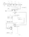
図3にデルタシグマ型分数分周PLLシンセサイザのブロック図を示す。まず、温度制御発振器(TCXO)7からの基準信号frefと、電圧制御発振器(VCO)1の出力信号foを可変分周器2Aにより分周した信号fdivとの位相差を位相比較器(PD)3で検出する。そして、その位相差に応じたパルス幅の電圧パルスが位相比較器3からチャージポンプ回路(CP)4に送られる。
FIG. 3 shows a block diagram of a delta sigma type fractional frequency division PLL synthesizer. First, the phase difference between the reference signal fref from the temperature controlled oscillator (TCXO) 7 and the signal fdiv obtained by dividing the output signal fo of the voltage controlled oscillator (VCO) 1 by the
チャージポンプ回路4は、位相比較器3の出力に応じて、電流の吐き出し、吸い込み、もしくはハイインピーダンス(Hi−Z)の状態のいずれかとなるチャージポンプ出力電流Icpを出力する。このチャージポンプ出力電流Icpはループフィルタ(ローパスフィルタ)5で平滑化および電圧変換されて、電圧制御発振器1の制御電圧となる。
The
電圧制御発振器1の出力信号foは、可変分周器2Aにより分周され、比較信号fdivとして位相比較器3へフィードバックされる。したがって電圧制御発振器1の出力信号foは、可変分周器2Aの分周比をM+(K/L)、基準信号frefの周波数をfrefとすれば以下のように表される。
The output signal fo of the voltage controlled
fo = M+(K/L) × fref ……(1)
M,K,L:正整数値 M:整数部分周比 K/L:小数点部分周比
可変分周器2Aは、整数部分周比Mの値を入力する整数分周比入力端子と、分周比をMからM+1に変化させる信号を入力する分周比切替端子とを有し、分周比がM、(M+1)に切り替え可能な構成となっている。具体的には、可変分周器2Aは、通常は分周比をMとし、分周比切替端子に分周比切替信号が入力されたときにのみ分周比を(M+1)とすることによって、平均的な分周比M+(K/L)を実現するものである。
fo = M + (K / L) × fref (1)
M, K, L: Positive integer value M: Integer partial frequency ratio K / L: Decimal point partial frequency ratio The
このような分周比の変化は、デルタシグマ部を構成するL値アキュムレータ11で実現することができる。すなわち、L値アキュムレータ11のオーバーフロー信号9を分周比切替端子に入力することにより、L値アキュムレータ11にオーバーフロー信号9が発生したときにのみ分周比を(M+1)とすることによって、平均的な分周比M+(K/L)を実現するものである。 Such a change in the frequency division ratio can be realized by the L value accumulator 11 constituting the delta sigma unit. That is, by inputting the overflow signal 9 of the L value accumulator 11 to the frequency division ratio switching terminal, the frequency division ratio is set to (M + 1) only when the overflow signal 9 is generated in the L value accumulator 11, thereby obtaining an average. A high frequency division ratio M + (K / L) is realized.
L値アキュムレータ11は、累算値が値Lとなると、オーバーフロー信号9を発生するもので、K値15を一方の入力とするL値加算器12と、L値加算器12の出力を基準信号frefで保持し、保持値をL値加算器12に他方の入力として与えるデータラッチ13とからなる。このL値アキュムレータ11は、基準信号frefに等しいクロックにより値Kずつ出力値が増加し、L値加算器12がオーバーフローした時に分周比がM+1となる。オーバーフロー信号9が発生しない時、分周比はMを保つ(例えば、非特許文献1参照)。 The L value accumulator 11 generates an overflow signal 9 when the accumulated value reaches the value L. The L value adder 12 having the K value 15 as one input and the output of the L value adder 12 as the reference signal It consists of a data latch 13 that holds it as fref and gives the hold value to the L-value adder 12 as the other input. The output value of the L value accumulator 11 increases by a value K by a clock equal to the reference signal fref, and the frequency division ratio becomes M + 1 when the L value adder 12 overflows. When the overflow signal 9 is not generated, the frequency division ratio is maintained at M (see, for example, Non-Patent Document 1).
ここで、図4を用いて、デルタシグマ部の動作原理を説明する。図4には、分周比=K/L=1/8の場合における、基準信号frefと、加算器12に入力されるK値15と、データラッチ12の出力14と、加算器12の出力10と、オーバーフロー信号9と、可変分周器2Aの分周比とが示されている。
Here, the operation principle of the delta-sigma unit will be described with reference to FIG. FIG. 4 shows the reference signal fref, the K value 15 input to the adder 12, the output 14 of the data latch 12, and the output of the adder 12 when the frequency division ratio = K / L = 1/8. 10, overflow signal 9, and frequency division ratio of
分数分周PLLシンセサイザでは、一般的な可変分周器2Aの分周比を時間的に変化させ、平均値として分数値の分周比を実現する。基準信号frefの1周期=1/frefを1クロック時間とすると、Lクロック時間(期間T)の間に1度だけ分周比がMからM+1に変化する。この時、期間Tにおける分周比の平均値は、M+(1/L)で示される。この分数部分の項の(1/L)は、(K/L)に拡張して考えることができ、K=1,2,3…とすることによって、(1/L)ステップで分周比を設定できる。
In the fractional frequency division PLL synthesizer, the frequency division ratio of the general
また一般的に、デルタシグマ回路を複数個接続した“MASH”を形成する事により、デルタシグマ構成のノイズ特性の改善が図られることが知られている(例えば、非特許文献2参照)。
しかし、上記先行技術の構成では、下に示した(a)、(b)、(c)が主な原因となり、電圧制御発振器1の出力信号foより、Δf=fref×(K/L)離調した周波数にスプリアスが発生していた。
However, in the configuration of the above prior art, the following causes (a), (b), and (c) are the main causes, and Δf = fref × (K / L) away from the output signal fo of the voltage controlled
(a) オーバーフロー信号9の周期性
(b) L値アキュムレータ11の周期的動作ノイズのチャージポンプ回路4等への漏れ込み
(c) 小数点部分周比(K/L)が、1/2nの場合
(a)については、L値アキュムレータ11を多段に接続することで、原理的に対策は可能である。
(A) Periodicity of overflow signal 9 (b) Leakage of periodic operation noise of L-value accumulator 11 into
しかし、(b)が原因で発生するスプリアスのうち、Δfが小さい(電圧制御発振器1の出力信号foに近い周波数)場合のスプリアス、すなわちループフィルタ5で減衰させることのできない低周波スプリアスについては根本的対策が無かった。
However, among the spurious generated due to (b), the spurious when Δf is small (frequency close to the output signal fo of the voltage controlled oscillator 1), that is, the low-frequency spurious that cannot be attenuated by the
また、(c)については、原理的にスプリアスが発生し易いという問題があった。 Further, (c) has a problem that spurious components are likely to occur in principle.
したがって、本発明の目的は、L値アキュムレータの周期的動作ノイズに起因するスプリアス、特に従来ループフィルタで除去することができなかった低周波スプリアスを十分に減衰させることができるデルタシグマ型分数分周PLLシンセサイザを提供することである。 Accordingly, an object of the present invention is to provide a delta-sigma type fractional frequency division that can sufficiently attenuate spurious due to periodic operation noise of an L-value accumulator, in particular, low-frequency spurious that could not be removed by a conventional loop filter. It is to provide a PLL synthesizer.
本発明のデルタシグマ型分数分周PLLシンセサイザは、電圧制御発振器(1)と、分周比がM(Mは正整数)、(M+1)、(M−1)に切り替え可能で電圧制御発振器(1)の出力信号foを分周する可変分周器(2)と、可変分周器(2)の出力信号fdivと基準信号frefの位相比較を行う位相比較器(4)と、位相比較器(4)の出力信号を平滑して電圧制御発振器(1)にフィードバックするループフィルタ(5)と、値L以下(Lは正整数)の値K1(K1は正整数)を累算する第1のL値アキュムレータ(31)と、値L以下の値K2(K2は正整数、K2<K1)を累算する第2のL値アキュムレータ(30)と、第1のL値アキュムレータ(31)のオーバーフロー信号から第2のL値アキュムレータ(30)のオーバーフロー信号を減じる加算器(29)とを備えている。 The delta-sigma fractional frequency division PLL synthesizer of the present invention includes a voltage controlled oscillator (1) and a voltage controlled oscillator (M is a positive integer), (M + 1), and (M-1) that can be switched to a voltage controlled oscillator ( 1) a variable frequency divider (2) that divides the output signal fo, a phase comparator (4) that performs phase comparison between the output signal fdiv of the variable frequency divider (2) and the reference signal fref, and a phase comparator A loop filter (5) for smoothing the output signal of (4) and feeding back to the voltage controlled oscillator (1), and a first value K1 (K1 is a positive integer) less than or equal to a value L (L is a positive integer). L value accumulator (31), a second L value accumulator (30) for accumulating a value K2 or less of value L (K2 is a positive integer, K2 <K1), and a first L value accumulator (31) The second L-value accumulator (30) is turned off from the overflow signal. It includes reducing the bar flow signal adder and (29).
そして、このデルタシグマ型分数分周PLLシンセサイザは、値K1,K2を、K1−K2=Kを満たし、かつ値K(Kは正整数)より大きな値に設定し、加算器(29)の出力信号を可変分周器(2)に分周比切替信号として与えることにより、加算器(29)の出力信号が零値のときに可変分周器(2)の分周比をMに設定し、加算器(29)の出力信号が正値のときに可変分周器(2)の分周比を(M+1)に設定し、加算器(29)の出力信号が負値のときに可変分周器(2)の分周比を(M−1)に設定し、それによって可変分周器(2)の平均的な分周比をM+(K/L)にする。 The delta-sigma fractional frequency division PLL synthesizer sets the values K1 and K2 to values that satisfy K1−K2 = K and is larger than the value K (K is a positive integer), and outputs the adder (29). By supplying the signal to the variable frequency divider (2) as a frequency division ratio switching signal, the frequency division ratio of the variable frequency divider (2) is set to M when the output signal of the adder (29) is zero. When the output signal of the adder (29) is a positive value, the division ratio of the variable frequency divider (2) is set to (M + 1), and when the output signal of the adder (29) is a negative value, The frequency division ratio of the frequency divider (2) is set to (M-1), and thereby the average frequency division ratio of the variable frequency divider (2) is set to M + (K / L).
ここで、第1のL値アキュムレータ(31)は、例えば値K1(K1は正整数)を一方の入力とする第1のL値加算器(22)と、第1のL値加算器(22)の出力を基準信号fref、もしくは可変分周器(2)の出力信号で保持し、保持値を第1のL値加算器(22)に他方の入力として与える第1のデータラッチ(24)とからなり、第2のL値アキュムレータ(30)は、例えば値K2(K2は正整数)を一方の入力とする第2のL値加算器(23)と、第2のL値加算器(23)の出力を基準信号fref、もしくは可変分周器(2)の出力信号で保持し、保持値を第2のL値加算器(23に他方の入力として与える第2のデータラッチ(25)とからなる。 Here, the first L-value accumulator (31) includes, for example, a first L-value adder (22) having a value K1 (K1 is a positive integer) as one input, and a first L-value adder (22 ) Is held by the reference signal fref or the output signal of the variable frequency divider (2), and the held value is supplied to the first L-value adder (22) as the other input, the first data latch (24) The second L-value accumulator (30) includes, for example, a second L-value adder (23) having a value K2 (K2 is a positive integer) as one input, and a second L-value adder ( 23) is held by the reference signal fref or the output signal of the variable frequency divider (2), and the hold value is supplied to the second L value adder (23 as the other input to the second data latch (25) It consists of.
ここで、上記デルタシグマ型分数分周PLLシンセサイザの作用について説明する。上記(b)が原因で発生するスプリアスのうち、ループフィルタ(5)で減衰させることのできない低周波スプリアス対策として、従来1個で構成していたL値アキュムレータ(11)を、図1に示すように、2個で構成し、所望の分数分周比データK値(15)に対して、
K値(15)=K1値(18)−K2値(19) ……(2)
を満たすようなK1値(18)、K2値(19)(共に正整数値)を第1のL値アキュムレータ(31)及び第2のL値アキュムレータ(30)へ入力する。例えば、K値(15)=1を設定したい時、(2)式を満たすようなK1値(18)=5、K値2(19)=4を設定する。
Here, the operation of the delta-sigma type fractional frequency division PLL synthesizer will be described. FIG. 1 shows an L-value accumulator (11) that has conventionally been configured as a single low-frequency spurious countermeasure that cannot be attenuated by the loop filter (5) among the spurious generated due to the above (b). In this way, it is composed of two pieces, and for the desired fractional division ratio data K value (15),
K value (15) = K1 value (18) −K2 value (19) (2)
K1 value (18) and K2 value (19) (both are positive integer values) satisfying the above are input to the first L value accumulator (31) and the second L value accumulator (30). For example, when K value (15) = 1 is desired to be set, K1 value (18) = 5 and K value 2 (19) = 4 are set so as to satisfy equation (2).
これにより、第1のL値アキュムレータ1(31)及び第2のL値アキュムレータ2(30)の動作ノイズは、先行技術におけるΔf=fref×(1/L)といった低周波スプリアスから、Δf1=fref×(5/L)及びΔf2=fref×(4/L)といった高い周波数成分へ移行することになる。そのため、L値アキュムレータ(31,30)の周期的動作ノイズが原因で発生するスプリアスは、ループフィルタ(5)でほぼ完全に減衰させることができる。 As a result, the operation noise of the first L-value accumulator 1 (31) and the second L-value accumulator 2 (30) is reduced from the low-frequency spurious Δf = fref × (1 / L) in the prior art by Δf1 = fref. It shifts to high frequency components such as × (5 / L) and Δf2 = fref × (4 / L). Therefore, the spurious generated due to the periodic operation noise of the L-value accumulator (31, 30) can be attenuated almost completely by the loop filter (5).
また、本発明の高次デルタシグマ型分数分周PLLシンセサイザは、上記構成を有する本発明のデルタシグマ型分数分周PLLシンセサイザを含んで構成される。 The high-order delta-sigma type fractional frequency division PLL synthesizer of the present invention includes the delta-sigma type fractional frequency division PLL synthesizer of the present invention having the above-described configuration.
本発明のデルタシグマ型分数分周PLLシンセサイザによれば、第1および第2のL値アキュムレータを設け、第1および第2のL値アキュムレータのオーバーフロー信号の差を加算器でとり、加算器の出力信号で、分周比をM、M+1、M−1に切替可能な可変分周器の分周比を切り替えるようにしたことにより、第1および第2のL値アキュムレータの動作ノイズによって発生するスプリアスの周波数を先行技術よりも高い周波数成分へ移行させることができ、ループフィルタ(ローパスフィルタ)で除去することが容易となり、低スプリアス化を図ることができる。 According to the delta-sigma fractional frequency division PLL synthesizer of the present invention, the first and second L-value accumulators are provided, the difference between the overflow signals of the first and second L-value accumulators is taken by the adder, This is caused by the operation noise of the first and second L-value accumulators by switching the frequency dividing ratio of the variable frequency divider that can switch the frequency dividing ratio to M, M + 1, and M−1. The spurious frequency can be shifted to a higher frequency component than in the prior art, and can be easily removed by a loop filter (low-pass filter), thereby reducing spurious.
以下、本発明の実施の形態を、図面を参照しながら説明する。 Hereinafter, embodiments of the present invention will be described with reference to the drawings.
(実施の形態1)
本発明の実施の形態1のデルタシグマ型分数分周PLLシンセサイザについて、図1および図2を参照しながら説明する。
(Embodiment 1)
A delta-sigma fractional frequency division PLL synthesizer according to the first embodiment of the present invention will be described with reference to FIG. 1 and FIG.
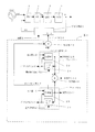
このデルタシグマ型分数分周PLLシンセサイザは、図1に示すように、温度制御発振器(TCXO)7からの基準信号frefと、電圧制御発振器(VCO)1の出力信号foを可変分周器2により分周した信号fdivとの位相差を位相比較器(PD)3で検出する。そして、その位相差に応じたパルス幅の電圧パルスが位相比較器3からチャージポンプ回路(CP)4に送られる。
As shown in FIG. 1, the delta-sigma fractional frequency division PLL synthesizer uses a
チャージポンプ回路4は、位相比較器3の出力に応じて、電流の吐き出し、吸い込み、もしくはハイインピーダンス(Hi−Z)の状態のいずれかとなるチャージポンプ出力電流Icpを出力する。このチャージポンプ出力電流Icpはループフィルタ(ローパスフィルタ)5で平滑化および電圧変換されて、電圧制御発振器1の制御電圧となる。
The
電圧制御発振器1の出力信号foは、可変分周器2により周波数foが分周され、比較信号fdivとして位相比較器3へフィードバックされる。したがって電圧制御発振器1の出力信号foは、可変分周器2の分周比をM+(K/L)、基準信号frefの周波数をfrefとすれば以下のように表される。
The output signal fo of the voltage controlled
fo = M+(K/L) × fref ……(3)
M,K,L:正整数値 M:整数部分周比 K/L:小数点部分周比
可変分周器2は、整数部分周比Mの値を入力する整数分周比入力端子と、分周比をMからM+1もしくはM−1に変化させる信号を入力する分周比切替端子とを有し、分周比がM、(M+1)、(M−1)に切り替え可能な構成となっている。具体的には、可変分周器2は、通常は分周比をMとし、分周比切替端子に分周比切替信号として正値の信号が入力されたときに分周比を(M+1)とし、負値の信号が入力されたときに分周比を(M−1)とし、零値の信号が入力されたときに分周比をMとすることによって、平均的な分周比M+(K/L)を実現するものである。
fo = M + (K / L) × fref (3)
M, K, L: Positive integer value M: Integer partial frequency ratio K / L: Decimal point partial frequency ratio The
このような分周比の変化は、デルタシグマ部X1を構成するL値アキュムレータ31,30および加算器29で実現することができる。すなわち、L値アキュムレータ31は、値L以下(Lは正整数)の値K1(K1は正整数)を累算し、L値アキュムレータ30は、値L以下の値K2(K2は正整数、K2<K1)を累算する。そして、加算器29は、L値アキュムレータ31のオーバーフロー信号16からL値アキュムレータ30のオーバーフロー信号17を減じてオーバーフロー信号9を出力する。
Such a change in the frequency division ratio can be realized by the
そして、値K1,K2を、K1−K2=Kを満たし、かつ値K(Kは正整数)より大きな値に設定する。また、加算器29の出力信号であるオーバーフロー信号9を分周比切替端子に入力することにより、加算器29のオーバーフロー信号9が零値のときに可変分周器2の分周比をMに設定し、加算器29のオーバーフロー信号9が正値のときに可変分周器2の分周比を(M+1)に設定し、加算器29のオーバーフロー信号9が負値のときに可変分周器2の分周比を(M−1)に設定し、それによって可変分周器2の平均的な分周比をM+(K/L)にする。
Then, the values K1 and K2 are set to values that satisfy K1−K2 = K and are larger than the value K (K is a positive integer). Further, by inputting the overflow signal 9 which is an output signal of the adder 29 to the frequency division ratio switching terminal, the frequency division ratio of the
L値アキュムレータ31は、累算値が値Lとなるとオーバーフロー信号16を発生するもので、分数分周比データK1値18を一方の入力とするL値加算器22と、L値加算器22の出力26を基準信号fref、もしくは可変分周器2の出力信号で保持し、保持値(データラッチ出力)20をL値加算器22に他方の入力として与えるデータラッチ24とからなる。このL値アキュムレータ31は、基準信号frefに等しいクロックによりK1値18ずつ出力値26が増加する。
The L value accumulator 31 generates an overflow signal 16 when the accumulated value reaches the value L. The
L値アキュムレータ30は、上記L値アキュムレータ31と同様に累算値が値Lとなるとオーバーフロー信号17を発生するもので、分数分周比データK2値19を一方の入力とするL値加算器23と、L値加算器23の出力27を基準信号fref、もしくは可変分周器2の出力信号で保持し、保持値(データラッチ出力)21をL値加算器23に他方の入力として与えるデータラッチ25とからなる。このL値アキュムレータ30は、基準信号frefに等しいクロックによりK2値19ずつ出力値27が増加する。
The
加算器28は、L値加算器22、23の出力を加算して出力10を発生する。この出力10は、本デルタシグマ型分数分周PLLシンセサイザを用いて高次デルタシグマ型分数分周PLLシンセサイザを構成するときに使用される。図1の構成に限っては、必要なものではない。
The adder 28 adds the outputs of the
以上のようなデルタシグマ部X1の構成によって、L値加算器22のみがオーバーフローしたときに分周比がM+1となり、L値加算器23のみがオーバーフローしたときに分周比がM−1となり、L値加算器22,23の両方がオーバーフローしたとき、あるいは、L値加算器22,23の両方ともオーバーフローしないときに、分周比がMに保たれる。
With the configuration of the delta sigma unit X1 as described above, the frequency division ratio becomes M + 1 when only the
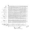
以下、図2を参照しながら、デルタシグマ部X1について、さらに詳しく説明する。図2には、分周比=K/L=1/8、K1=5、K2=4の場合における、基準信号frefと、K1値18と、データラッチ24の出力20と、L値加算器22の出力26と、オーバーフロー信号16と、K2値19と、データラッチ25の出力21と、L値加算器23の出力27と、オーバーフロー信号17と、加算器28の出力10と、オーバーフロー信号9と、可変分周器2の分周比とが示されている。
Hereinafter, the delta-sigma portion X1 will be described in more detail with reference to FIG. FIG. 2 shows the reference signal fref, the K1 value 18, the output 20 of the data latch 24, and the L value adder when the division ratio = K / L = 1/8, K1 = 5, and K2 = 4. 22 output 26, overflow signal 16, K2 value 19, output 21 of data latch 25, output 27 of
L値アキュムレータ31は、分数分周比データK1値18とデータラッチ24の出力20とが入力され、オーバーフロー信号16を出力するL値加算器22と、L値加算器22の出力26と基準信号frefとが入力されるデータラッチ24にて構成される。また、L値アキュムレータ30は、分数分周比データK2値19とデータラッチ25の出力21とが入力され、オーバーフロー信号17を出力するL値加算器23と、L値加算器23の出力27と基準信号frefとが入力されるデータラッチ25にて構成される。
The L value accumulator 31 receives the fractional division ratio data K1 value 18 and the output 20 of the data latch 24, and outputs an
加算器28は、L値加算器22の出力26からL値加算器23の出力27を減算し、加算出力10を出力し、加算器29は、L値加算器22のオーバーフロー信号16からL値加算器23のオーバーフロー信号17を減算し、オーバーフロー信号9を出力する。
The adder 28 subtracts the output 27 of the
先行技術の従来回路では、fref=200kHz、L=8で、K値(15)=1を設定する場合、L値アキュムレータ11の周期的動作ノイズが原因によるスプリアス成分は、
Δf=200kHz×(1/8)=25kHz
つまり、電圧制御発振器1の出力信号foより、25kHz離調した周波数にスプリアスが発生していた。
In the conventional circuit of the prior art, when setting K value (15) = 1 with fref = 200 kHz, L = 8, the spurious component due to the periodic operation noise of the L value accumulator 11 is
Δf = 200 kHz × (1/8) = 25 kHz
That is, spurious was generated at a frequency detuned by 25 kHz from the output signal fo of the voltage controlled
しかし、本発明の実施の形態の構成では、上記と同様の設定をしたい場合、例えば、K1値(18)=5、K2値(19)=4と設定する。ここで、K1値(18)及びK2値(19)は、前述の(2)式を満たし、かつ許容される大きな値(値Kより大きく、値L以下の値)に設定することで、アキュムレータ1(31)及びアキュムレータ2(30)の周期的動作ノイズ動作ノイズが原因によるスプリアス成分の離調周波数Δfは先行技術の場合に比べて大きくなる。そのため、ループフィルタ5で減衰させることが容易である。
However, in the configuration of the embodiment of the present invention, when the same setting as described above is desired, for example, K1 value (18) = 5 and K2 value (19) = 4 are set. Here, the K1 value (18) and the K2 value (19) satisfy the above-described expression (2) and are set to an allowable large value (a value larger than the value K and less than or equal to the value L). 1 (31) and periodic operation noise of accumulator 2 (30) The detuning frequency Δf of the spurious component due to the operation noise is larger than that in the prior art. Therefore, it is easy to attenuate with the
K1値(18)=5、K2値(19)=4でのL値アキュムレータ31及びL値アキュムレータ30の周期的動作ノイズが原因で発生するスプリアスの離調周波数は、
Δf1=200kHz×(5/8)=125kHz
Δf2=200kHz×(4/8)=100kHz
となり、従来と比べて高い周波数成分へ移行することが分かる。このため、L値アキュムレータ31及びL値アキュムレータ30の周期的動作ノイズが原因で発生するスプリアスは、ループフィルタ5でほぼ完全に減衰させることができる。
The spurious detuning frequency generated due to the periodic operation noise of the L value accumulator 31 and the
Δf1 = 200 kHz × (5/8) = 125 kHz
Δf2 = 200 kHz × (4/8) = 100 kHz
Thus, it can be seen that the frequency component shifts to a higher frequency than in the conventional case. For this reason, the spurious generated due to the periodic operation noise of the L value accumulator 31 and the
さらに、先行技術では、K/L=1/2nの分周比において低域のスプリアスが多くなることがあったが、今回の回路ではそれも緩和されるという効果がある。
(実施の形態2)
本発明の実施の形態2の高次デルタシグマ型分数分周PLLシンセサイザについて、図5を参照しながら説明する。
Furthermore, in the prior art, spurious in the low band may increase in the frequency division ratio of K / L = 1/2 n , but this circuit has the effect of alleviating this.
(Embodiment 2)
A high-order delta-sigma fractional frequency division PLL synthesizer according to
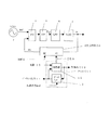
この高次デルタシグマ型分数分周PLLシンセサイザは、図5に示すように、実施の形態1に示したもの(符号X1で示す)と同じ構成の第1のデルタシグマ部X1に加えて、実施の形態1に示したもの(符号X1で示す)と同じ構成の第2のデルタシグマ部X2を設け、第2のデルタシグマX2への入力値Kを、実施の形態1で示したような条件に分配する分配器51を設ける。第2のデルタシグマ部X2への入力値Kは、第1のデルタシグマ部X1の加算出力10である。つまり、加算出力10が分配器51で、以下のように分配されて第2のデルタシグマ部X2へ入力される。
As shown in FIG. 5, the high-order delta-sigma fractional frequency division PLL synthesizer is implemented in addition to the first delta-sigma section X1 having the same configuration as that shown in the first embodiment (indicated by reference numeral X1). The second delta sigma unit X2 having the same configuration as that shown in the first embodiment (indicated by reference numeral X1) is provided, and the input value K to the second delta sigma X2 is set as the condition shown in the first embodiment. A distributor 51 is provided for distributing to each other. The input value K to the second delta sigma part X2 is the
分配器51は、加算出力10をK3値とK4値とに分配する。分配の仕方は、実施の形態1と同様にして、
“K3”−“K4”=“加算出力10”
かつ、“K4”<“K3”を満たし、かつ“K3”,“K4”ともに、“加算出力10”の値よりも大きな値(正整数)に設定される。
The distributor 51 distributes the
“K3” − “K4” = “
Further, “K4” <“K3” is satisfied, and “K3” and “K4” are both set to a value (positive integer) larger than the value of “
第2のデルタシグマ部X2の出力であるオーバーフロー信号54は微分器52で微分された後、加算器53でデルタシグマ部X1の出力であるオーバーフロー信号9と加算され、加算器53の出力信号が可変分周器2Bに分周比切替信号として与えられる。
The overflow signal 54 that is the output of the second delta sigma unit X2 is differentiated by the
ここで、デルタシグマ部X1,X2のオーバーフロー信号9,54は、図2に示したように、例えば…0,+1,−1,+1,0…と変化し、これを微分すると、つまり連続した2つの値の差をとると、…1,−2,+2,−1…となる。オーバーフロー信号9とオーバーフロー信号54の微分値とを加算すると、各値の組み合わせの中で加算結果の最大値は+3となり、最小値は−3となる。したがって、可変分周器2Bは、加算器53から入力される加算結果に応じて、分周比をM+3、M+2、M+1、M、M−1、M−2、M−3のいずれかに切り替えることになる。 Here, as shown in FIG. 2, the overflow signals 9 and 54 of the delta sigma parts X1 and X2 change, for example,..., 0, +1, −1, +1, 0. When the difference between the two values is taken,..., 1, -2, +2, -1. When the overflow signal 9 and the differential value of the overflow signal 54 are added, the maximum value of the addition result is +3 and the minimum value is −3 among the combinations of the values. Therefore, the variable frequency divider 2B switches the division ratio to any of M + 3, M + 2, M + 1, M, M-1, M-2, and M-3 according to the addition result input from the adder 53. It will be.
これにより、本発明の実施の形態でも、デルタシグマ回路を複数個接続した“MASH”を形成することができ、前述の非特許文献2に記載の効果と同様の効果が得られ、低ノイズ化に有利である。
As a result, even in the embodiment of the present invention, a “MASH” in which a plurality of delta-sigma circuits are connected can be formed, and the same effect as that described in
なお、実施の形態2は、2次の構成の例を示したが、3次以上の構成も同様に考えることができる。 Although the second embodiment shows an example of a second-order configuration, a third-order or higher-order configuration can be considered similarly.
本発明にかかるデルタシグマ型分数分周PLLシンセサイザは、低スプリアス化を図ることができるという効果が必要な携帯電話機などの移動体通信機器等の用途に適用できる。 The delta-sigma fractional frequency division PLL synthesizer according to the present invention can be applied to applications such as mobile communication devices such as mobile phones that require the effect of reducing spurious.
1 電圧制御発振器
2 可変分周器
3 位相比較器
4 チャージポンプ回路
5 ループフィルタ
7 温度制御発振器
8 M値
9 オーバーフロー信号
10 加算出力
11 アキュムレータ
12 加算器
13 データラッチ
14 データラッチ出力
15 K値
16 オーバーフロー信号
17 オーバーフロー信号
18 K1値
19 K2値
20 データラッチ出力
21 データラッチ出力
22 L値加算器
23 L値加算器
24 データラッチ
25 データラッチ
26 加算器出力
27 加算器出力
28 加算器
29 加算器
30,31 アキュムレータ
DESCRIPTION OF
Claims (3)
分周比がM(Mは正整数)、(M+1)、(M−1)に切り替え可能で前記電圧制御発振器の出力信号を分周する可変分周器と、
前記可変分周器の出力信号と基準信号の位相比較を行う位相比較器と、
前記位相比較器の出力信号を平滑して前記電圧制御発振器に与えるループフィルタと、
値L以下(Lは正整数)の値K1(K1は正整数)を累算する第1のL値アキュムレータと、
値L以下の値K2(K2は正整数、K2<K1)を累算する第2のL値アキュムレータと、
前記第1のL値アキュムレータのオーバーフロー信号から前記第2のL値アキュムレータのオーバーフロー信号を減じる加算器とを備え、
前記値K1,K2を、K1−K2=Kを満たし、かつ値K(Kは正整数)より大きな値に設定し、
前記加算器の出力信号を前記可変分周器に分周比切替信号として与えることにより、前記加算器の出力信号が零値のときに前記可変分周器の分周比をMに設定し、前記加算器の出力信号が正値のときに前記可変分周器の分周比を(M+1)に設定し、前記加算器の出力信号が負値のときに前記可変分周器の分周比を(M−1)に設定し、それによって前記可変分周器の平均的な分周比をM+(K/L)にすることを特徴とするデルタシグマ型分数分周PLLシンセサイザ。 A voltage controlled oscillator;
A variable frequency divider capable of switching the frequency division ratio to M (M is a positive integer), (M + 1), (M-1) and dividing the output signal of the voltage controlled oscillator;
A phase comparator for performing phase comparison between the output signal of the variable frequency divider and a reference signal;
A loop filter that smoothes the output signal of the phase comparator and supplies the output signal to the voltage controlled oscillator;
A first L value accumulator that accumulates a value K1 (K1 is a positive integer) less than or equal to a value L (L is a positive integer);
A second L-value accumulator that accumulates a value K2 (K2 is a positive integer, K2 <K1) less than or equal to a value L;
An adder for subtracting the overflow signal of the second L value accumulator from the overflow signal of the first L value accumulator;
The values K1 and K2 are set to a value satisfying K1−K2 = K and larger than the value K (K is a positive integer);
By giving the output signal of the adder to the variable divider as a division ratio switching signal, when the output signal of the adder is zero, the division ratio of the variable divider is set to M, The division ratio of the variable frequency divider is set to (M + 1) when the output signal of the adder is a positive value, and the division ratio of the variable frequency divider is set when the output signal of the adder is a negative value. Is set to (M-1), and thereby the average frequency division ratio of the variable frequency divider is set to M + (K / L), a delta-sigma type fractional frequency division PLL synthesizer.
A high-order delta-sigma fractional frequency division PLL synthesizer comprising the delta-sigma fractional frequency division PLL synthesizer according to claim 1.
Priority Applications (5)
| Application Number | Priority Date | Filing Date | Title |
|---|---|---|---|
| JP2003411776A JP4064338B2 (en) | 2003-12-10 | 2003-12-10 | Delta-sigma fractional frequency division PLL synthesizer |
| US10/581,262 US20070103239A1 (en) | 2003-12-10 | 2004-12-09 | Delta-sigma type fraction pll synthesizer |
| CNA2004800368234A CN1890881A (en) | 2003-12-10 | 2004-12-09 | Delta-sigma type fraction division pll synthesizer |
| EP04820278A EP1693967A4 (en) | 2003-12-10 | 2004-12-09 | Delta-sigma type fraction division pll synthesizer |
| PCT/JP2004/018405 WO2005057793A1 (en) | 2003-12-10 | 2004-12-09 | Delta-sigma type fraction division pll synthesizer |
Applications Claiming Priority (1)
| Application Number | Priority Date | Filing Date | Title |
|---|---|---|---|
| JP2003411776A JP4064338B2 (en) | 2003-12-10 | 2003-12-10 | Delta-sigma fractional frequency division PLL synthesizer |
Publications (2)
| Publication Number | Publication Date |
|---|---|
| JP2005175780A JP2005175780A (en) | 2005-06-30 |
| JP4064338B2 true JP4064338B2 (en) | 2008-03-19 |
Family
ID=34675007
Family Applications (1)
| Application Number | Title | Priority Date | Filing Date |
|---|---|---|---|
| JP2003411776A Expired - Fee Related JP4064338B2 (en) | 2003-12-10 | 2003-12-10 | Delta-sigma fractional frequency division PLL synthesizer |
Country Status (5)
| Country | Link |
|---|---|
| US (1) | US20070103239A1 (en) |
| EP (1) | EP1693967A4 (en) |
| JP (1) | JP4064338B2 (en) |
| CN (1) | CN1890881A (en) |
| WO (1) | WO2005057793A1 (en) |
Families Citing this family (53)
| Publication number | Priority date | Publication date | Assignee | Title |
|---|---|---|---|---|
| KR100900864B1 (en) * | 2003-12-11 | 2009-06-04 | 모사이드 테크놀로지스, 인코포레이티드 | High output impedance charge pump for PLL/DLL |
| US7098707B2 (en) * | 2004-03-09 | 2006-08-29 | Altera Corporation | Highly configurable PLL architecture for programmable logic |
| KR100638894B1 (en) | 2006-01-02 | 2006-10-27 | 삼성전기주식회사 | Programable frequency divider using sigma-delta modulator |
| US7579902B2 (en) * | 2006-12-11 | 2009-08-25 | Atmel Corporation | Charge pump for generation of multiple output-voltage levels |
| JP4827764B2 (en) | 2007-02-20 | 2011-11-30 | 富士通セミコンダクター株式会社 | Fractional frequency division PLL device and control method thereof |
| CN101060330B (en) * | 2007-03-22 | 2011-06-22 | 郑尧 | A broken number frequency division synthesizer |
| US7633349B2 (en) * | 2007-04-04 | 2009-12-15 | Altera Corporation | Phase frequency detectors generating minimum pulse widths |
| JP2008275407A (en) * | 2007-04-27 | 2008-11-13 | Nec Electronics Corp | Semiconductor integrated circuit and method of inspecting semiconductor integrated circuit |
| GB2452748A (en) * | 2007-09-13 | 2009-03-18 | Cambridge Silicon Radio Ltd | Digital phase locked loop |
| CN101465645B (en) * | 2007-12-19 | 2010-12-15 | 中国科学院微电子研究所 | Decimal/integer frequency divider |
| US7893788B2 (en) * | 2008-02-19 | 2011-02-22 | Mediatek Inc. | Charge pump-based frequency modulator |
| US8085097B2 (en) * | 2008-05-06 | 2011-12-27 | Hittite Microwave Corporation | Integrated ramp, sweep fractional frequency synthesizer on an integrated circuit chip |
| EP2131499A1 (en) * | 2008-06-02 | 2009-12-09 | Seiko Epson Corporation | Digital accumulator with configurable resolution and Sigma-Delta modulator comprising it |
| JP4562787B2 (en) | 2008-07-30 | 2010-10-13 | ルネサスエレクトロニクス株式会社 | PLL circuit |
| JP4787870B2 (en) * | 2008-10-02 | 2011-10-05 | 日本電波工業株式会社 | Frequency synthesizer |
| US7786773B2 (en) * | 2008-10-06 | 2010-08-31 | Himax Technologies Limited | Phase-locked loop circuit |
| GB0821772D0 (en) * | 2008-11-28 | 2009-01-07 | Zarlink Semiconductor Inc | Soft reference switch for phase locked loop |
| JP5180793B2 (en) * | 2008-11-28 | 2013-04-10 | キヤノン株式会社 | Clock generation circuit, integrated circuit, and imaging sensor |
| US8259890B2 (en) * | 2009-02-18 | 2012-09-04 | Mediatek Inc. | Phase-locked loop circuit and related phase locking method |
| US8031008B2 (en) * | 2009-04-21 | 2011-10-04 | Mediatek Inc. | PLL with loop bandwidth calibration circuit |
| US7973612B2 (en) * | 2009-04-26 | 2011-07-05 | Qualcomm Incorporated | Supply-regulated phase-locked loop (PLL) and method of using |
| US8169265B2 (en) * | 2009-04-29 | 2012-05-01 | Mediatek Inc. | Phase lock loop circuits |
| US8063707B2 (en) * | 2009-05-08 | 2011-11-22 | Mediatek Inc. | Phase locked loop |
| US8368480B2 (en) * | 2009-06-24 | 2013-02-05 | Mediatek Inc. | Phase locked loop circuits and gain calibration methods thereof |
| CN101964658B (en) * | 2009-07-23 | 2012-10-17 | 财团法人工业技术研究院 | Digital phase-locked loop and digital-phase frequency detector thereof |
| CN102045063B (en) * | 2009-10-12 | 2013-10-30 | 晨星软件研发(深圳)有限公司 | Control circuit for voltage controlled oscillator of phase locked loop and control method of control circuit |
| CN102045060B (en) * | 2009-10-13 | 2017-03-01 | 晨星软件研发(深圳)有限公司 | Portable control device and its method |
| CN102045061B (en) * | 2009-10-16 | 2013-04-24 | 晨星软件研发(深圳)有限公司 | Loop bandwidth control device and method of phase locked loop |
| CN102045064B (en) * | 2009-10-20 | 2013-03-13 | 群联电子股份有限公司 | Phase locked loop and voltage controlled oscillator |
| CN101699769B (en) * | 2009-10-27 | 2012-04-04 | 华为技术有限公司 | Phase-locked loop bandwidth calibration method, system and electronic device |
| CN101789785B (en) * | 2010-01-11 | 2011-12-28 | 清华大学 | fully integrated phase-locked loop frequency synthesizer |
| CN101917191A (en) * | 2010-02-11 | 2010-12-15 | 深圳市国微电子股份有限公司 | Phase-locked loop chip |
| JP4933635B2 (en) * | 2010-02-19 | 2012-05-16 | 日本電波工業株式会社 | PLL circuit |
| CN101800542B (en) * | 2010-03-11 | 2012-07-04 | 复旦大学 | CMOS ultra-wideband prescaler |
| CN102255614B (en) * | 2010-05-20 | 2017-04-19 | 晨星软件研发(深圳)有限公司 | Clock generation circuit and clock generation method |
| CN101873133B (en) * | 2010-06-21 | 2012-06-06 | 王珲 | Frequency locking method applied to communication clock recovery and electric device structure thereof |
| CN101931404A (en) * | 2010-06-21 | 2010-12-29 | 胡伟东 | Phase lock technique-based microwave carbon testing frequency synthesizer |
| CN101917187A (en) * | 2010-07-16 | 2010-12-15 | 中国兵器工业第二○六研究所 | Stepped frequency signal generation method based on frequency selective output of initialize switch of phase-locked loop |
| CN101924553B (en) * | 2010-09-15 | 2012-06-13 | 复旦大学 | Complementary metal oxide semiconductor (CMOS) ultra-wide-band divide-by-2 frequency divider structure |
| CN101986568B (en) * | 2010-10-22 | 2012-11-14 | 江苏锦丰电子有限公司 | Steady state phase-locking error-free phase locking system and phase locking method |
| US8400199B2 (en) * | 2010-11-26 | 2013-03-19 | Mediatek Inc. | Charge pump, phase frequency detector and charge pump methods |
| CN102006068A (en) * | 2010-11-30 | 2011-04-06 | 江汉大学 | Improved rubidium atom frequency scale |
| CN102006064B (en) * | 2010-12-16 | 2012-05-30 | 电子科技大学 | Voltage controlled oscillator (VCO) with high tuning linearity |
| CN102185607B (en) * | 2011-01-25 | 2013-11-06 | 上海华为技术有限公司 | Phase difference detection method, device and circuit in phase-locked loop circuit |
| CN102045062B (en) * | 2011-01-27 | 2013-02-06 | 中山大学 | Digital phase-locked loop based on Cordic algorithm |
| CN102130679B (en) * | 2011-04-12 | 2013-01-30 | 广州润芯信息技术有限公司 | Active RC (Resistance-Capacitance) filter bandwidth calibration method |
| KR101179646B1 (en) | 2011-04-18 | 2012-09-04 | 한국과학기술원 | Frequency synthesizer, method for generating output frequency and method for calibrating conversion gain |
| CN102299709A (en) * | 2011-04-27 | 2011-12-28 | 广州润芯信息技术有限公司 | High precision pulse width comparator based on time-to-digit conversion |
| US9632526B2 (en) * | 2012-11-26 | 2017-04-25 | Microchip Technology Incorporated | Microcontroller with digital clock source |
| US9036762B2 (en) | 2013-04-16 | 2015-05-19 | Silicon Laboratories Inc. | Generating compatible clocking signals |
| CN103414469A (en) * | 2013-06-27 | 2013-11-27 | 深圳市创成微电子有限公司 | RFID fractional-N PLL technology |
| JP6247546B2 (en) * | 2014-01-24 | 2017-12-13 | アイコム株式会社 | Fractional N frequency synthesizer and setting method thereof |
| CN108549046A (en) * | 2018-05-23 | 2018-09-18 | 中国电子科技集团公司第四十研究所 | The automatic test approach of module occurs in broadband multiple spot reference signal for labview |
Family Cites Families (5)
| Publication number | Priority date | Publication date | Assignee | Title |
|---|---|---|---|---|
| US5070310A (en) * | 1990-08-31 | 1991-12-03 | Motorola, Inc. | Multiple latched accumulator fractional N synthesis |
| FR2763196B1 (en) * | 1997-05-07 | 1999-07-30 | Thomson Csf | CONSISTENT FREQUENCY SYNTHESIZER WITH PHASE LOOP AND NOT FRACTIONAL |
| FR2765419B1 (en) * | 1997-06-27 | 1999-09-17 | Thomson Csf | DEVICE FOR GENERATING ANALOG SIGNALS FROM ANALOG-TO-DIGITAL CONVERTERS, PARTICULARLY FOR DIRECT DIGITAL SYNTHESIS |
| US5777521A (en) * | 1997-08-12 | 1998-07-07 | Motorola Inc. | Parallel accumulator fractional-n frequency synthesizer |
| JP2001298363A (en) * | 2000-04-17 | 2001-10-26 | Matsushita Electric Ind Co Ltd | Frequency synthesizer device and mobile radio equipment using the same |
-
2003
- 2003-12-10 JP JP2003411776A patent/JP4064338B2/en not_active Expired - Fee Related
-
2004
- 2004-12-09 US US10/581,262 patent/US20070103239A1/en not_active Abandoned
- 2004-12-09 WO PCT/JP2004/018405 patent/WO2005057793A1/en active Application Filing
- 2004-12-09 EP EP04820278A patent/EP1693967A4/en not_active Withdrawn
- 2004-12-09 CN CNA2004800368234A patent/CN1890881A/en active Pending
Also Published As
| Publication number | Publication date |
|---|---|
| US20070103239A1 (en) | 2007-05-10 |
| EP1693967A4 (en) | 2007-10-03 |
| EP1693967A1 (en) | 2006-08-23 |
| CN1890881A (en) | 2007-01-03 |
| JP2005175780A (en) | 2005-06-30 |
| WO2005057793A1 (en) | 2005-06-23 |
Similar Documents
| Publication | Publication Date | Title |
|---|---|---|
| JP4064338B2 (en) | Delta-sigma fractional frequency division PLL synthesizer | |
| JP2844389B2 (en) | Synthesis of multistage latch accumulator fraction N | |
| US8008955B2 (en) | Semiconductor device | |
| JP4493887B2 (en) | Fractional N frequency synthesizer and method of operating the same | |
| JP2750639B2 (en) | Latch accumulator fractional N synthesis with residual error reduction | |
| US7274231B1 (en) | Low jitter frequency synthesizer | |
| WO2017053372A1 (en) | Apparatus and methods for fractional-n phase-locked loops with multi-phase oscillators | |
| EP1609243A1 (en) | Method and system of jitter compensation | |
| CA2233831A1 (en) | Digital-sigma fractional-n synthesizer | |
| US8406364B2 (en) | Fractional frequency divider PLL device and control method thereof | |
| JPH0951268A (en) | Frequency synthesizer | |
| US9019016B2 (en) | Accumulator-type fractional N-PLL synthesizer and control method thereof | |
| KR100880422B1 (en) | Fractional-N Frequency Synthesizer With Fractional Compensation Method | |
| JP3611589B2 (en) | Fractional N divider | |
| CN101399551A (en) | Multi-stage noise regulating type modulator and frequency synthesizer | |
| KR100801034B1 (en) | Method of reducing noise in sigma-delta modulation using delayed clock signals and fractional-n pll using the method | |
| JP2020136824A (en) | Fractional frequency divider and frequency synthesizer | |
| US20120139654A1 (en) | Frequency synthesizer | |
| JP4050298B2 (en) | PLL circuit ΣΔ modulator | |
| JP2015100081A (en) | Spread spectrum clock generator and control method thereof | |
| JP3792706B2 (en) | PLL circuit ΣΔ modulator | |
| JP4037212B2 (en) | Semiconductor device | |
| CN110506394B (en) | Frequency generator | |
| WO2008041216A1 (en) | A sigma-delta modulator | |
| JP2012204883A (en) | Accumulator type fractional n-pll synthesizer and method of controlling the same |
Legal Events
| Date | Code | Title | Description |
|---|---|---|---|
| RD04 | Notification of resignation of power of attorney |
Free format text: JAPANESE INTERMEDIATE CODE: A7424 Effective date: 20060517 |
|
| A621 | Written request for application examination |
Free format text: JAPANESE INTERMEDIATE CODE: A621 Effective date: 20061023 |
|
| TRDD | Decision of grant or rejection written | ||
| A01 | Written decision to grant a patent or to grant a registration (utility model) |
Free format text: JAPANESE INTERMEDIATE CODE: A01 Effective date: 20071204 |
|
| A61 | First payment of annual fees (during grant procedure) |
Free format text: JAPANESE INTERMEDIATE CODE: A61 Effective date: 20071226 |
|
| FPAY | Renewal fee payment (event date is renewal date of database) |
Free format text: PAYMENT UNTIL: 20110111 Year of fee payment: 3 |
|
| FPAY | Renewal fee payment (event date is renewal date of database) |
Free format text: PAYMENT UNTIL: 20110111 Year of fee payment: 3 |
|
| FPAY | Renewal fee payment (event date is renewal date of database) |
Free format text: PAYMENT UNTIL: 20120111 Year of fee payment: 4 |
|
| LAPS | Cancellation because of no payment of annual fees |