EP1524697A2 - Festkörperbildsensor und dessen Verfahren zur Herstellung - Google Patents
Festkörperbildsensor und dessen Verfahren zur Herstellung Download PDFInfo
- Publication number
- EP1524697A2 EP1524697A2 EP04024618A EP04024618A EP1524697A2 EP 1524697 A2 EP1524697 A2 EP 1524697A2 EP 04024618 A EP04024618 A EP 04024618A EP 04024618 A EP04024618 A EP 04024618A EP 1524697 A2 EP1524697 A2 EP 1524697A2
- Authority
- EP
- European Patent Office
- Prior art keywords
- region
- type
- edge
- gate electrode
- positioned adjacent
- Prior art date
- Legal status (The legal status is an assumption and is not a legal conclusion. Google has not performed a legal analysis and makes no representation as to the accuracy of the status listed.)
- Granted
Links
Images


Classifications
-
- H—ELECTRICITY
- H10—SEMICONDUCTOR DEVICES; ELECTRIC SOLID-STATE DEVICES NOT OTHERWISE PROVIDED FOR
- H10F—INORGANIC SEMICONDUCTOR DEVICES SENSITIVE TO INFRARED RADIATION, LIGHT, ELECTROMAGNETIC RADIATION OF SHORTER WAVELENGTH OR CORPUSCULAR RADIATION
- H10F39/00—Integrated devices, or assemblies of multiple devices, comprising at least one element covered by group H10F30/00, e.g. radiation detectors comprising photodiode arrays
- H10F39/10—Integrated devices
- H10F39/12—Image sensors
-
- H—ELECTRICITY
- H10—SEMICONDUCTOR DEVICES; ELECTRIC SOLID-STATE DEVICES NOT OTHERWISE PROVIDED FOR
- H10F—INORGANIC SEMICONDUCTOR DEVICES SENSITIVE TO INFRARED RADIATION, LIGHT, ELECTROMAGNETIC RADIATION OF SHORTER WAVELENGTH OR CORPUSCULAR RADIATION
- H10F39/00—Integrated devices, or assemblies of multiple devices, comprising at least one element covered by group H10F30/00, e.g. radiation detectors comprising photodiode arrays
- H10F39/80—Constructional details of image sensors
- H10F39/803—Pixels having integrated switching, control, storage or amplification elements
-
- H—ELECTRICITY
- H10—SEMICONDUCTOR DEVICES; ELECTRIC SOLID-STATE DEVICES NOT OTHERWISE PROVIDED FOR
- H10F—INORGANIC SEMICONDUCTOR DEVICES SENSITIVE TO INFRARED RADIATION, LIGHT, ELECTROMAGNETIC RADIATION OF SHORTER WAVELENGTH OR CORPUSCULAR RADIATION
- H10F30/00—Individual radiation-sensitive semiconductor devices in which radiation controls the flow of current through the devices, e.g. photodetectors
- H10F30/20—Individual radiation-sensitive semiconductor devices in which radiation controls the flow of current through the devices, e.g. photodetectors the devices having potential barriers, e.g. phototransistors
-
- H—ELECTRICITY
- H10—SEMICONDUCTOR DEVICES; ELECTRIC SOLID-STATE DEVICES NOT OTHERWISE PROVIDED FOR
- H10F—INORGANIC SEMICONDUCTOR DEVICES SENSITIVE TO INFRARED RADIATION, LIGHT, ELECTROMAGNETIC RADIATION OF SHORTER WAVELENGTH OR CORPUSCULAR RADIATION
- H10F39/00—Integrated devices, or assemblies of multiple devices, comprising at least one element covered by group H10F30/00, e.g. radiation detectors comprising photodiode arrays
- H10F39/80—Constructional details of image sensors
- H10F39/807—Pixel isolation structures
Definitions
- the present invention relates to a solid-state imaging device that uses an active MOS sensor.
- the present invention relates to a solid-state imaging device that enables readout at a low voltage and suppresses image defects (especially for example, white flaws and dark current).
- a solid-state imaging device using an active MOS sensor is configured such that a signal detected by a photodiode is amplified at a transistor in each pixel, and the solid-state imaging device is characterized by its high sensitivity.
- a most serious problem for the solid-state imaging device is a reverse-direction leakage current at a pn junction of a silicon semiconductor. This leakage current, which cannot be isolated from a signal current generated by incident light, becomes a noise and degrades the performance of the solid-state imaging device. This leakage current is caused in part by stress applied to the silicon substrate.
- FIG. 4 illustrates a silicon substrate 101 on which a gate insulating film 102 and a gate electrode 103 are formed.
- a gate-edge region 104 extending from an edge of the gate electrode 103 to the periphery was applied with stress that causes leakage current in the vicinity of the surface of the silicon substrate 101.
- a crystal defect 105 caused by stress was observed inside this gate-edge region 104.
- Such a crystal defect was not found in the part under the gate electrode 103.
- the conventional emphasis has been to suppress a leakage current generated at the part of the gate-edge region 104.
- this gate-edge region 104 is also a via point for electric charge at a time of reading signal charge out from a photodiode formed at the left of the gate electrode 103 in FIG. 3, a condition for facilitating the charge readout and a condition for suppressing the leakage current will be traded off in the design.
- an object has been to suppress a leakage current 108 that flows into the photodiode region 107 from the area under the gate electrode 103, and at the same time, to design the trade-off for facilitating readout of signal charge from the photodiode.
- FIG. 6 is a cross-sectional view of a cell of a conventional solid-state imaging device (see, for example, JP 11 (1999)-274450).
- a P-well 2 is formed of a Si substrate 1, and a N-type photodiode region 3 for a photoelectric conversion is formed inside the P-well 2.
- One edge of the gate electrode 4 is positioned adjacent to the N-type photodiode region 3.
- the lower part of the gate electrode 4 has a MOS transistor structure, in which a gate oxide film 5 and a threshold controlling implantation region 6 for a transistor are formed.
- a N-type drain region 7 is formed adjacent to the other edge of the gate electrode 4. Electrons that have been photoelectrically converted are stored in the N-type photodiode region 3, transferred to the N-type drain region 7, and detected as signals.
- a high-concentration P-type diffusion layer 8 is formed adjacent to one edge of the gate electrode 4, and a high-concentration P-type diffusion layer 9 is formed adjacent to the P-type diffusion layer 8.
- the high-concentration P-type diffusion layer 9 is a surface-shield layer for shielding the upper surface of the photodiode, and it is formed to suppress influences of crystal defects and metal pollution on the interface state of the Si-SiO 2 interface. Elements such as the photodiode and a plurality of MOS transistors are isolated from each other by an element-isolating portion 10.
- the concentration of the P-type diffusion layer 8 in the vicinity of the gate is set lower than the concentration of the P-type diffusion layer 9 forming the surface-shield layer, thereby improving the readout characteristic.
- concentration of the P-type diffusion layer 8 in the vicinity of the gate electrode 4 is reduced, the interface state of the Si-SiO 2 interface and the active level in the Si substrate 1 cannot be inactivated sufficiently, which may cause problems such as image defects (e.g., white flaws and dark current).
- a solid-state imaging device of the present invention includes: a plurality of N-type photodiode regions that are formed inside a P-type well of a Si substrate in order to photoelectrically convert incident light; a gate electrode having one edge positioned adjacent to each of the photodiode regions; a N-type drain region positioned adjacent to the other edge of the gate electrode; an element-isolating portion having a shallow trench isolation structure for isolating respectively a plurality of elements composed of groups of the respective photodiode regions and MOS transistors; and a gate oxide film having a thickness of not more than 10 nm.
- the gate electrode has one edge portion overlapping the photodiode region; and a first region, a second region and a third region are formed on a surface portion extending from the upper portion of the photodiode region to the drain region in conditions such that the first region is disposed at a predetermined distance from one edge of the gate electrode and has a P-type first concentration C1, the second region is disposed with one edge positioned adjacent to the first region and the other edge overlapping the gate electrode in a certain region and has a P-type second concentration C2, and the third region is disposed with one edge positioned adjacent to the second region and the other edge positioned adjacent to the drain region and has a P-type third concentration C3, with the respective concentrations are in a relationship of C1 > C2 > C3 or C1 ⁇ C2 > C3.
- a method of manufacturing a solid-state imaging device relates to a method of manufacturing the solid-state imaging device having the above-described configuration, characterized in that the respective concentrations are adjusted by controlling a dose of ion implantation for forming the P-type diffusion layers.
- Another method of manufacturing a solid-state imaging device relates to a method of manufacturing the solid-state imaging device having the above-described configuration, characterized in that the P-type diffusion layer of the first region is formed so as to extend to the part below the gate electrode by a heat treatment in order to form a P-type diffusion layer of the second region, thereby differentiating the concentration C1 from the concentration C2.
- FIG. 1 is a cross-sectional view showing a cell structure of a solid-state imaging device according to a first embodiment of the present invention.
- FIG. 2 is a cross-sectional view showing a cell structure of a solid-state imaging device according to a second embodiment of the present invention.
- FIG. 3 is a cross-sectional view showing a cell structure of a solid-state imaging device according to a third embodiment of the present invention.
- FIG. 4 is a cross-sectional view for explaining the occurrence of image defects in the vicinity of a gate of a solid-state imaging device.
- FIG. 5 is a cross-sectional view for explaining the occurrence of an image defects for a case of thin gate insulating film.
- FIG. 6 is a cross-sectional view showing a cell structure of a conventional solid-state imaging device.
- the concentrations of the P-type diffusion layers of the P-type second and P-type third regions separately by controlling the concentrations of the P-type diffusion layers of the P-type second and P-type third regions separately, a low voltage operation of not higher than 3 V is allowed, and furthermore, image defects can be decreased remarkably.
- a bottom of the P-type diffusion layer of the second region is positioned deeper than bottoms of the P-type diffusion layers of the first region and of the third region. It is also preferable that the bottoms of the P-type diffusion layers of the second region and of the third region are positioned deeper than the bottom of the P-type diffusion layer of the first region.
- an acceleration energy of ion implantation during formation of the second region is increased in comparison to formation of the first region and of the third region, thereby positioning the bottom of the P-type diffusion layer of the second region deeper than the bottoms of the P-type diffusion layers of the first region and of the third region.
- acceleration energies of ion implantation during formation of the second region and the third region are increased in comparison to formation of the first region, thereby positioning the bottoms of the P-type diffusion layers of the second region and of the third region deeper than the bottom of the P-type diffusion layer of the first region.
- the heat treatment can be performed in a step of forming a gate oxide film. It is also preferable that a further step of annealing at 1050°C for at least 30 minutes is carried out in the step of forming the gate oxide film.
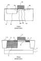
- FIG. 1 is a cross-sectional view showing a cell structure of a solid-state imaging device according to a first embodiment.
- a N-type photodiode region 3 for photoelectrically converting incident light is formed inside a P-well 2 of a Si substrate 1.
- a gate electrode 4 is disposed so that one edge thereof forms an overlapping region with the photodiode region 3. Adjacent to the other edge of the gate electrode 4, an N-type drain region 7 is formed.
- a gate oxide film 5 having a thickness of not more than 10 nm is formed under the gate electrode 4, a gate oxide film 5 having a thickness of not more than 10 nm is formed.
- An element-isolating portion 10 having a STI (Shallow Trench Isolation) structure isolates respective elements composed of a photodiode and a plurality of MOS transistors.
- STI Shallow Trench Isolation
- a P-type first region 11 having a P-type first concentration and a P-type second region 12 having a P-type second concentration are formed.
- a P-type third region 13 having a P-type third concentration is formed in a region adjacent to the P-type second region 12 and extending to the drain region 7.
- the P-type first region 11 is formed in a region extending from the outer periphery of the photodiode region 3 to a position separated by a predetermined distance from a near edge of the gate electrode 4.
- the predetermined distance that is the distance between the gate electrode 4 and the P-type first region 11, is preferably 0.2 ⁇ m or more.
- the P-type second region 12 has an edge positioned adjacent to the P-type first region 11, while the other edge overlaps the gate electrode 4.
- the P-type second region 12 can be positioned adjacent to the gate electrode 4 without overlapping.
- the concentrations of the P-type first region 11 the P-type second region 12 and the P-type third region 13 are denoted as C1, C2 and C3 respectively
- the relationship of the concentrations is expressed as C1 > C2 > C3 or C1 ⁇ C2>C3.
- a dose of a B + ion implantation for forming the P-type second region 12 is 2.0 ⁇ 10 12 ions/cm 2 or more.
- a P-type second region 12 with a concentration lower than that of the P-type first region 11 can be formed by diffusing the high-concentration P-type first region 11 to the lower part of the gate electrode 4 by a heat diffusion.
- a solid-state imaging device capable of being operated at a low voltage can be obtained by controlling a B + dose for the P-type third region 13.
- a length (i.e., the transverse distance in FIG.1) of the overlapping region between the gate electrode 4 and the photodiode region 3 is designed preferably to a range from 0.1 ⁇ m to 0.3 ⁇ m.
- a B + dose for forming the P-type third region 13 is smaller than that for the P-type second region 12.
- FIG. 2 is a cross-sectional view showing a cell structure of a solid-state imaging device of a second embodiment. Identical reference numbers are used for components common to those of the first embodiment described above, and detailed explanation will be omitted for these components.
- a P-type second-A region 14 is formed in place of the P-type second region 12 of the first embodiment.
- the P-type seoond-A region 14 is characterized in that a bottom of the P-type diffusion layer is positioned deeper than bottoms of the P-type diffusion layers of the P-type first region 11 and the P-type third region 13.
- the acceleration energy of ion implantation is increased.
- E1 denotes an acceleration energy of the P-type first region 11
- E2A denotes an acceleration energy of the P-type second-A region 14
- E3 denotes an acceleration energy of the P-type third region 13
- the respective acceleration energies are in a relationship of E1 ⁇ E3 ⁇ E2A.
- FIG. 3 is a cross-sectional view showing a cell structure of a solid-state imaging device according to a third embodiment. Identical reference numbers are used for components common to those of the first embodiment described above, and detailed explanation will be omitted for these components.
- a P-type second-B region 15 and a P-type third-A region 16 are formed in place of the P-type second region 12 and the P-type third region 13 of the first embodiment.
- This embodiment is characterized in that bottoms of the P-type diffusion layers of the P-type second-B region 15 and of the P-type third-A region 16 are positioned deeper than the bottoms of the P-type first region 11.
- the energy of ion implantation during formation of the P-type diffusion layers is increased so as to position the bottoms of the P-type diffusion layers of the P-type second-B region 15 and of the P-type third A region 16 deeper than the bottom of the P-type first region 11.
- the respective acceleration energies are in a relationship of E1 ⁇ E2B ⁇ E3A.
- the heat treatment can be conducted by heat applied in a step of forming a gate oxide film 5.
- the effect can be increased further by adding an annealing step to the gate oxidation step.
- the annealing temperature is preferably 1050°C or higher.
- a solid-state imaging device includes: a plurality of N-type photodiode regions formed inside a P-type well; a gate electrode having one edge being positioned adjacent to each of the photodiode regions; a N-type drain region positioned adjacent to the other edge of the gate electrode; an element-isolating portion having a STI structure, and a gate oxide film having a thickness of not more than 10 nm.
- One edge of the gate electrode overlaps the photodiode region.
- First, second and third regions are formed on a surface portion extending from the photodiode region to the drain region, in conditions such that the first region is disposed with a predetermined distance from one edge of the gate electrode and has a P-type first concentration C1, the second region is disposed with one edge positioned adjacent to the first region and the other edge overlapping the gate electrode and has a P-type second concentration C2, and the third region is disposed with one edge positioned adjacent to the second region and the other edge positioned adjacent to the drain region and has a P-type third concentration C3, wherein C1 > C2 > C3 or C1 ⁇ C2 > C3.
- the readout characteristic at a low voltage is satisfactory, and image defects such as white flaws and dark current are suppressed sufficiently.
Landscapes
- Solid State Image Pick-Up Elements (AREA)
- Transforming Light Signals Into Electric Signals (AREA)
Applications Claiming Priority (2)
| Application Number | Priority Date | Filing Date | Title |
|---|---|---|---|
| JP2003356590 | 2003-10-16 | ||
| JP2003356590A JP4758061B2 (ja) | 2003-10-16 | 2003-10-16 | 固体撮像装置およびその製造方法 |
Publications (3)
| Publication Number | Publication Date |
|---|---|
| EP1524697A2 true EP1524697A2 (de) | 2005-04-20 |
| EP1524697A3 EP1524697A3 (de) | 2006-10-18 |
| EP1524697B1 EP1524697B1 (de) | 2011-01-12 |
Family
ID=34373600
Family Applications (1)
| Application Number | Title | Priority Date | Filing Date |
|---|---|---|---|
| EP04024618A Expired - Lifetime EP1524697B1 (de) | 2003-10-16 | 2004-10-15 | Festkörperbildsensor und Verfahren zu dessen Herstellung |
Country Status (7)
| Country | Link |
|---|---|
| US (2) | US7030433B2 (de) |
| EP (1) | EP1524697B1 (de) |
| JP (1) | JP4758061B2 (de) |
| KR (1) | KR100597124B1 (de) |
| CN (1) | CN100435341C (de) |
| DE (1) | DE602004030984D1 (de) |
| TW (1) | TW200515591A (de) |
Cited By (1)
| Publication number | Priority date | Publication date | Assignee | Title |
|---|---|---|---|---|
| EP1748489A3 (de) * | 2005-07-29 | 2007-09-05 | Fujitsu Limited | Halbleiterbildaufnahmeanordnung und Herstellungsverfahren dafür |
Families Citing this family (29)
| Publication number | Priority date | Publication date | Assignee | Title |
|---|---|---|---|---|
| JP4282521B2 (ja) * | 2004-03-26 | 2009-06-24 | 株式会社東芝 | 固体撮像装置及び画像処理機能を有する携帯電話機 |
| US7115924B1 (en) * | 2005-06-03 | 2006-10-03 | Avago Technologies Sensor Ip Pte. Ltd. | Pixel with asymmetric transfer gate channel doping |
| KR100699849B1 (ko) | 2005-06-21 | 2007-03-27 | 삼성전자주식회사 | 국부적인 불순물 영역을 갖는 cmos 이미지 소자 및 그제조방법 |
| KR100871714B1 (ko) * | 2005-12-05 | 2008-12-05 | 한국전자통신연구원 | 트랜스퍼 트랜지스터 및 이를 구비한 저잡음 이미지 센서 |
| US7999342B2 (en) * | 2007-09-24 | 2011-08-16 | Taiwan Semiconductor Manufacturing Company, Ltd | Image sensor element for backside-illuminated sensor |
| US8183628B2 (en) | 2007-10-29 | 2012-05-22 | Unisantis Electronics Singapore Pte Ltd. | Semiconductor structure and method of fabricating the semiconductor structure |
| KR100997326B1 (ko) * | 2007-12-27 | 2010-11-29 | 주식회사 동부하이텍 | 이미지 센서 및 그 제조방법 |
| US8598650B2 (en) | 2008-01-29 | 2013-12-03 | Unisantis Electronics Singapore Pte Ltd. | Semiconductor device and production method therefor |
| JP5317343B2 (ja) | 2009-04-28 | 2013-10-16 | ユニサンティス エレクトロニクス シンガポール プライベート リミテッド | 半導体装置及びその製造方法 |
| JP4832541B2 (ja) * | 2009-03-17 | 2011-12-07 | シャープ株式会社 | 固体撮像素子および電子情報機器 |
| JP5493430B2 (ja) * | 2009-03-31 | 2014-05-14 | ソニー株式会社 | 固体撮像装置とその製造方法、及び電子機器 |
| JP5356970B2 (ja) | 2009-10-01 | 2013-12-04 | ユニサンティス エレクトロニクス シンガポール プライベート リミテッド | 半導体装置 |
| WO2011111662A1 (ja) | 2010-03-08 | 2011-09-15 | 日本ユニサンティスエレクトロニクス株式会社 | 固体撮像装置 |
| US8487357B2 (en) * | 2010-03-12 | 2013-07-16 | Unisantis Electronics Singapore Pte Ltd. | Solid state imaging device having high sensitivity and high pixel density |
| JP5066590B2 (ja) | 2010-06-09 | 2012-11-07 | ユニサンティス エレクトロニクス シンガポール プライベート リミテッド | 半導体装置とその製造方法 |
| JP5087655B2 (ja) | 2010-06-15 | 2012-12-05 | ユニサンティス エレクトロニクス シンガポール プライベート リミテッド | 半導体装置及びその製造方法 |
| FR2971887B1 (fr) * | 2011-02-17 | 2013-02-22 | St Microelectronics Sa | Photosite a transfert de charges amélioré |
| US8564034B2 (en) | 2011-09-08 | 2013-10-22 | Unisantis Electronics Singapore Pte. Ltd. | Solid-state imaging device |
| US8669601B2 (en) | 2011-09-15 | 2014-03-11 | Unisantis Electronics Singapore Pte. Ltd. | Method for producing semiconductor device and semiconductor device having pillar-shaped semiconductor |
| US8772175B2 (en) | 2011-12-19 | 2014-07-08 | Unisantis Electronics Singapore Pte. Ltd. | Method for manufacturing semiconductor device and semiconductor device |
| US8916478B2 (en) | 2011-12-19 | 2014-12-23 | Unisantis Electronics Singapore Pte. Ltd. | Method for manufacturing semiconductor device and semiconductor device |
| US8748938B2 (en) | 2012-02-20 | 2014-06-10 | Unisantis Electronics Singapore Pte. Ltd. | Solid-state imaging device |
| JP5458135B2 (ja) * | 2012-03-28 | 2014-04-02 | シャープ株式会社 | 固体撮像素子の製造方法 |
| US9287319B2 (en) * | 2012-11-16 | 2016-03-15 | Sri International | CMOS multi-pinned (MP) pixel |
| JP6184761B2 (ja) * | 2013-06-11 | 2017-08-23 | 浜松ホトニクス株式会社 | 固体撮像装置 |
| JP2017092084A (ja) * | 2015-11-02 | 2017-05-25 | キヤノン株式会社 | 撮像素子及びその製造方法 |
| US10777591B2 (en) * | 2017-08-15 | 2020-09-15 | Taiwan Semiconductor Manufacturing Co., Ltd. | Image sensor device |
| JP2020021775A (ja) * | 2018-07-30 | 2020-02-06 | キヤノン株式会社 | 固体撮像装置及び撮像システム |
| CN109817654A (zh) * | 2019-02-14 | 2019-05-28 | 德淮半导体有限公司 | 图像传感器及其形成方法 |
Citations (1)
| Publication number | Priority date | Publication date | Assignee | Title |
|---|---|---|---|---|
| JPH11274459A (ja) | 1998-03-20 | 1999-10-08 | Toshiba Corp | 固体撮像装置 |
Family Cites Families (16)
| Publication number | Priority date | Publication date | Assignee | Title |
|---|---|---|---|---|
| JPH07161958A (ja) * | 1993-12-09 | 1995-06-23 | Nec Corp | 固体撮像装置 |
| KR100192954B1 (ko) * | 1996-07-18 | 1999-06-15 | 김광호 | 수직형 전달게이트를 가지는 전하결합형 고체촬상소자 및 그 제조방법 |
| US6100556A (en) * | 1997-11-14 | 2000-08-08 | Motorola Inc. | Method of forming a semiconductor image sensor and structure |
| US6023081A (en) * | 1997-11-14 | 2000-02-08 | Motorola, Inc. | Semiconductor image sensor |
| JPH11274450A (ja) * | 1998-03-19 | 1999-10-08 | Toshiba Corp | 固体撮像装置 |
| US6690423B1 (en) | 1998-03-19 | 2004-02-10 | Kabushiki Kaisha Toshiba | Solid-state image pickup apparatus |
| JP2000077647A (ja) * | 1998-09-01 | 2000-03-14 | Matsushita Electronics Industry Corp | 固体撮像装置及びその製造方法 |
| JP4284752B2 (ja) * | 1999-05-31 | 2009-06-24 | ソニー株式会社 | 固体撮像素子 |
| JP3934827B2 (ja) * | 1999-06-30 | 2007-06-20 | 株式会社東芝 | 固体撮像装置 |
| JP4419238B2 (ja) * | 1999-12-27 | 2010-02-24 | ソニー株式会社 | 固体撮像素子及びその製造方法 |
| JP2002198510A (ja) * | 2000-12-27 | 2002-07-12 | Sony Corp | 固体撮像素子およびその製造方法 |
| US20020106865A1 (en) * | 2001-02-05 | 2002-08-08 | Tai-Ju Chen | Method of forming shallow trench isolation |
| DE10132430B4 (de) * | 2001-07-04 | 2010-02-18 | Advanced Micro Devices, Inc., Sunnyvale | Verfahren zur Bildung einer dünnen Oxidschicht mit einer verbesserten Zuverlässigkeit auf einer Halbleiteroberfläche |
| JP3723124B2 (ja) * | 2001-12-14 | 2005-12-07 | 株式会社東芝 | 固体撮像装置 |
| JP4541666B2 (ja) * | 2002-06-20 | 2010-09-08 | 三星電子株式会社 | イメージセンサ及びその製造方法 |
| KR100508086B1 (ko) * | 2002-09-11 | 2005-08-17 | 삼성전자주식회사 | 씨모스 이미지 센서 및 그 제조방법 |
-
2003
- 2003-10-16 JP JP2003356590A patent/JP4758061B2/ja not_active Expired - Fee Related
-
2004
- 2004-10-06 TW TW093130214A patent/TW200515591A/zh unknown
- 2004-10-08 US US10/962,261 patent/US7030433B2/en not_active Expired - Fee Related
- 2004-10-12 CN CNB2004100856884A patent/CN100435341C/zh not_active Expired - Fee Related
- 2004-10-15 KR KR1020040082654A patent/KR100597124B1/ko not_active Expired - Fee Related
- 2004-10-15 DE DE602004030984T patent/DE602004030984D1/de not_active Expired - Lifetime
- 2004-10-15 EP EP04024618A patent/EP1524697B1/de not_active Expired - Lifetime
-
2006
- 2006-02-10 US US11/351,526 patent/US7329557B2/en not_active Expired - Lifetime
Patent Citations (1)
| Publication number | Priority date | Publication date | Assignee | Title |
|---|---|---|---|---|
| JPH11274459A (ja) | 1998-03-20 | 1999-10-08 | Toshiba Corp | 固体撮像装置 |
Cited By (3)
| Publication number | Priority date | Publication date | Assignee | Title |
|---|---|---|---|---|
| EP1748489A3 (de) * | 2005-07-29 | 2007-09-05 | Fujitsu Limited | Halbleiterbildaufnahmeanordnung und Herstellungsverfahren dafür |
| US7846758B2 (en) | 2005-07-29 | 2010-12-07 | Fujitsu Semiconductor Limited | Semiconductor imaging device and fabrication process thereof |
| US8008106B2 (en) | 2005-07-29 | 2011-08-30 | Fujitsu Semiconductor Limited | Semiconductor imaging device and fabrication process thereof |
Also Published As
| Publication number | Publication date |
|---|---|
| EP1524697B1 (de) | 2011-01-12 |
| US7030433B2 (en) | 2006-04-18 |
| US20050082631A1 (en) | 2005-04-21 |
| TW200515591A (en) | 2005-05-01 |
| US20060128052A1 (en) | 2006-06-15 |
| US7329557B2 (en) | 2008-02-12 |
| KR20050036819A (ko) | 2005-04-20 |
| CN100435341C (zh) | 2008-11-19 |
| EP1524697A3 (de) | 2006-10-18 |
| KR100597124B1 (ko) | 2006-07-05 |
| DE602004030984D1 (de) | 2011-02-24 |
| JP4758061B2 (ja) | 2011-08-24 |
| CN1610126A (zh) | 2005-04-27 |
| JP2005123395A (ja) | 2005-05-12 |
Similar Documents
| Publication | Publication Date | Title |
|---|---|---|
| EP1524697B1 (de) | Festkörperbildsensor und Verfahren zu dessen Herstellung | |
| US7224003B2 (en) | Solid-state image pickup apparatus | |
| EP2284896B1 (de) | Festkörper-Bildaufnahmevorrichtung mit einer Photodiode und MOSFET | |
| US7855407B2 (en) | CMOS image sensor and method for manufacturing the same | |
| US8008106B2 (en) | Semiconductor imaging device and fabrication process thereof | |
| JPH07161958A (ja) | 固体撮像装置 | |
| US7304338B2 (en) | Solid-state image sensor and method for fabricating the same | |
| US6492668B2 (en) | Solid imaging device and production method thereof | |
| US7005315B2 (en) | Method and fabricating complementary metal-oxide semiconductor image sensor with reduced etch damage | |
| JP2921567B1 (ja) | 固体撮像装置およびその製造方法 | |
| US6566722B1 (en) | Photo sensor in a photo diode on a semiconductor wafer | |
| KR20050025073A (ko) | 고체 촬상 장치 및 카메라 | |
| US6541329B1 (en) | Method for making an active pixel sensor | |
| US7485939B2 (en) | Solid-state imaging device having a defect control layer and an inversion layer between a trench and a charge accumulating area | |
| JP2002110955A (ja) | Cmosイメージセンサ及びcmosイメージセンサの製造方法 | |
| US20050158897A1 (en) | Image sensor device and method of fabricating the same | |
| JP2008153566A (ja) | 固体撮像装置及びその製造方法 | |
| US7645652B2 (en) | CMOS image sensor and method for fabricating the same | |
| JP2007201088A (ja) | 固体撮像素子 | |
| JP2007201087A (ja) | 固体撮像素子の製造方法及び固体撮像素子 | |
| JP2007234874A (ja) | 固体撮像装置の製造方法 |
Legal Events
| Date | Code | Title | Description |
|---|---|---|---|
| PUAI | Public reference made under article 153(3) epc to a published international application that has entered the european phase |
Free format text: ORIGINAL CODE: 0009012 |
|
| AK | Designated contracting states |
Kind code of ref document: A2 Designated state(s): AT BE BG CH CY CZ DE DK EE ES FI FR GB GR HU IE IT LI LU MC NL PL PT RO SE SI SK TR |
|
| AX | Request for extension of the european patent |
Extension state: AL HR LT LV MK |
|
| PUAL | Search report despatched |
Free format text: ORIGINAL CODE: 0009013 |
|
| AK | Designated contracting states |
Kind code of ref document: A3 Designated state(s): AT BE BG CH CY CZ DE DK EE ES FI FR GB GR HU IE IT LI LU MC NL PL PT RO SE SI SK TR |
|
| AX | Request for extension of the european patent |
Extension state: AL HR LT LV MK |
|
| 17P | Request for examination filed |
Effective date: 20070330 |
|
| AKX | Designation fees paid |
Designated state(s): DE FR GB NL |
|
| 17Q | First examination report despatched |
Effective date: 20070807 |
|
| RAP1 | Party data changed (applicant data changed or rights of an application transferred) |
Owner name: PANASONIC CORPORATION |
|
| GRAP | Despatch of communication of intention to grant a patent |
Free format text: ORIGINAL CODE: EPIDOSNIGR1 |
|
| GRAC | Information related to communication of intention to grant a patent modified |
Free format text: ORIGINAL CODE: EPIDOSCIGR1 |
|
| GRAS | Grant fee paid |
Free format text: ORIGINAL CODE: EPIDOSNIGR3 |
|
| GRAA | (expected) grant |
Free format text: ORIGINAL CODE: 0009210 |
|
| AK | Designated contracting states |
Kind code of ref document: B1 Designated state(s): DE FR GB NL |
|
| REG | Reference to a national code |
Ref country code: GB Ref legal event code: FG4D |
|
| REF | Corresponds to: |
Ref document number: 602004030984 Country of ref document: DE Date of ref document: 20110224 Kind code of ref document: P |
|
| REG | Reference to a national code |
Ref country code: DE Ref legal event code: R096 Ref document number: 602004030984 Country of ref document: DE Effective date: 20110224 |
|
| REG | Reference to a national code |
Ref country code: NL Ref legal event code: VDEP Effective date: 20110112 |
|
| PG25 | Lapsed in a contracting state [announced via postgrant information from national office to epo] |
Ref country code: NL Free format text: LAPSE BECAUSE OF FAILURE TO SUBMIT A TRANSLATION OF THE DESCRIPTION OR TO PAY THE FEE WITHIN THE PRESCRIBED TIME-LIMIT Effective date: 20110112 |
|
| PLBE | No opposition filed within time limit |
Free format text: ORIGINAL CODE: 0009261 |
|
| STAA | Information on the status of an ep patent application or granted ep patent |
Free format text: STATUS: NO OPPOSITION FILED WITHIN TIME LIMIT |
|
| 26N | No opposition filed |
Effective date: 20111013 |
|
| PGFP | Annual fee paid to national office [announced via postgrant information from national office to epo] |
Ref country code: FR Payment date: 20111103 Year of fee payment: 8 |
|
| REG | Reference to a national code |
Ref country code: DE Ref legal event code: R097 Ref document number: 602004030984 Country of ref document: DE Effective date: 20111013 |
|
| GBPC | Gb: european patent ceased through non-payment of renewal fee |
Effective date: 20121015 |
|
| REG | Reference to a national code |
Ref country code: FR Ref legal event code: ST Effective date: 20130628 |
|
| PG25 | Lapsed in a contracting state [announced via postgrant information from national office to epo] |
Ref country code: GB Free format text: LAPSE BECAUSE OF NON-PAYMENT OF DUE FEES Effective date: 20121015 Ref country code: DE Free format text: LAPSE BECAUSE OF NON-PAYMENT OF DUE FEES Effective date: 20130501 |
|
| REG | Reference to a national code |
Ref country code: DE Ref legal event code: R119 Ref document number: 602004030984 Country of ref document: DE Effective date: 20130501 |
|
| PG25 | Lapsed in a contracting state [announced via postgrant information from national office to epo] |
Ref country code: FR Free format text: LAPSE BECAUSE OF NON-PAYMENT OF DUE FEES Effective date: 20121031 |