EP1524642A2 - Anzeigevorrichtung - Google Patents
Anzeigevorrichtung Download PDFInfo
- Publication number
- EP1524642A2 EP1524642A2 EP04023948A EP04023948A EP1524642A2 EP 1524642 A2 EP1524642 A2 EP 1524642A2 EP 04023948 A EP04023948 A EP 04023948A EP 04023948 A EP04023948 A EP 04023948A EP 1524642 A2 EP1524642 A2 EP 1524642A2
- Authority
- EP
- European Patent Office
- Prior art keywords
- discharge
- sustain
- pulse
- discharge cell
- cell
- Prior art date
- Legal status (The legal status is an assumption and is not a legal conclusion. Google has not performed a legal analysis and makes no representation as to the accuracy of the status listed.)
- Withdrawn
Links
Images





Classifications
-
- G—PHYSICS
- G09—EDUCATION; CRYPTOGRAPHY; DISPLAY; ADVERTISING; SEALS
- G09G—ARRANGEMENTS OR CIRCUITS FOR CONTROL OF INDICATING DEVICES USING STATIC MEANS TO PRESENT VARIABLE INFORMATION
- G09G3/00—Control arrangements or circuits, of interest only in connection with visual indicators other than cathode-ray tubes
- G09G3/20—Control arrangements or circuits, of interest only in connection with visual indicators other than cathode-ray tubes for presentation of an assembly of a number of characters, e.g. a page, by composing the assembly by combination of individual elements arranged in a matrix no fixed position being assigned to or needed to be assigned to the individual characters or partial characters
- G09G3/2007—Display of intermediate tones
- G09G3/2059—Display of intermediate tones using error diffusion
-
- G—PHYSICS
- G09—EDUCATION; CRYPTOGRAPHY; DISPLAY; ADVERTISING; SEALS
- G09G—ARRANGEMENTS OR CIRCUITS FOR CONTROL OF INDICATING DEVICES USING STATIC MEANS TO PRESENT VARIABLE INFORMATION
- G09G3/00—Control arrangements or circuits, of interest only in connection with visual indicators other than cathode-ray tubes
- G09G3/20—Control arrangements or circuits, of interest only in connection with visual indicators other than cathode-ray tubes for presentation of an assembly of a number of characters, e.g. a page, by composing the assembly by combination of individual elements arranged in a matrix no fixed position being assigned to or needed to be assigned to the individual characters or partial characters
- G09G3/22—Control arrangements or circuits, of interest only in connection with visual indicators other than cathode-ray tubes for presentation of an assembly of a number of characters, e.g. a page, by composing the assembly by combination of individual elements arranged in a matrix no fixed position being assigned to or needed to be assigned to the individual characters or partial characters using controlled light sources
- G09G3/28—Control arrangements or circuits, of interest only in connection with visual indicators other than cathode-ray tubes for presentation of an assembly of a number of characters, e.g. a page, by composing the assembly by combination of individual elements arranged in a matrix no fixed position being assigned to or needed to be assigned to the individual characters or partial characters using controlled light sources using luminous gas-discharge panels, e.g. plasma panels
- G09G3/288—Control arrangements or circuits, of interest only in connection with visual indicators other than cathode-ray tubes for presentation of an assembly of a number of characters, e.g. a page, by composing the assembly by combination of individual elements arranged in a matrix no fixed position being assigned to or needed to be assigned to the individual characters or partial characters using controlled light sources using luminous gas-discharge panels, e.g. plasma panels using AC panels
- G09G3/291—Control arrangements or circuits, of interest only in connection with visual indicators other than cathode-ray tubes for presentation of an assembly of a number of characters, e.g. a page, by composing the assembly by combination of individual elements arranged in a matrix no fixed position being assigned to or needed to be assigned to the individual characters or partial characters using controlled light sources using luminous gas-discharge panels, e.g. plasma panels using AC panels controlling the gas discharge to control a cell condition, e.g. by means of specific pulse shapes
- G09G3/294—Control arrangements or circuits, of interest only in connection with visual indicators other than cathode-ray tubes for presentation of an assembly of a number of characters, e.g. a page, by composing the assembly by combination of individual elements arranged in a matrix no fixed position being assigned to or needed to be assigned to the individual characters or partial characters using controlled light sources using luminous gas-discharge panels, e.g. plasma panels using AC panels controlling the gas discharge to control a cell condition, e.g. by means of specific pulse shapes for lighting or sustain discharge
-
- G—PHYSICS
- G09—EDUCATION; CRYPTOGRAPHY; DISPLAY; ADVERTISING; SEALS
- G09G—ARRANGEMENTS OR CIRCUITS FOR CONTROL OF INDICATING DEVICES USING STATIC MEANS TO PRESENT VARIABLE INFORMATION
- G09G3/00—Control arrangements or circuits, of interest only in connection with visual indicators other than cathode-ray tubes
- G09G3/20—Control arrangements or circuits, of interest only in connection with visual indicators other than cathode-ray tubes for presentation of an assembly of a number of characters, e.g. a page, by composing the assembly by combination of individual elements arranged in a matrix no fixed position being assigned to or needed to be assigned to the individual characters or partial characters
- G09G3/2007—Display of intermediate tones
- G09G3/2018—Display of intermediate tones by time modulation using two or more time intervals
- G09G3/2022—Display of intermediate tones by time modulation using two or more time intervals using sub-frames
-
- G—PHYSICS
- G09—EDUCATION; CRYPTOGRAPHY; DISPLAY; ADVERTISING; SEALS
- G09G—ARRANGEMENTS OR CIRCUITS FOR CONTROL OF INDICATING DEVICES USING STATIC MEANS TO PRESENT VARIABLE INFORMATION
- G09G3/00—Control arrangements or circuits, of interest only in connection with visual indicators other than cathode-ray tubes
- G09G3/20—Control arrangements or circuits, of interest only in connection with visual indicators other than cathode-ray tubes for presentation of an assembly of a number of characters, e.g. a page, by composing the assembly by combination of individual elements arranged in a matrix no fixed position being assigned to or needed to be assigned to the individual characters or partial characters
- G09G3/2007—Display of intermediate tones
- G09G3/2044—Display of intermediate tones using dithering
- G09G3/2051—Display of intermediate tones using dithering with use of a spatial dither pattern
-
- G—PHYSICS
- G09—EDUCATION; CRYPTOGRAPHY; DISPLAY; ADVERTISING; SEALS
- G09G—ARRANGEMENTS OR CIRCUITS FOR CONTROL OF INDICATING DEVICES USING STATIC MEANS TO PRESENT VARIABLE INFORMATION
- G09G3/00—Control arrangements or circuits, of interest only in connection with visual indicators other than cathode-ray tubes
- G09G3/20—Control arrangements or circuits, of interest only in connection with visual indicators other than cathode-ray tubes for presentation of an assembly of a number of characters, e.g. a page, by composing the assembly by combination of individual elements arranged in a matrix no fixed position being assigned to or needed to be assigned to the individual characters or partial characters
- G09G3/22—Control arrangements or circuits, of interest only in connection with visual indicators other than cathode-ray tubes for presentation of an assembly of a number of characters, e.g. a page, by composing the assembly by combination of individual elements arranged in a matrix no fixed position being assigned to or needed to be assigned to the individual characters or partial characters using controlled light sources
- G09G3/28—Control arrangements or circuits, of interest only in connection with visual indicators other than cathode-ray tubes for presentation of an assembly of a number of characters, e.g. a page, by composing the assembly by combination of individual elements arranged in a matrix no fixed position being assigned to or needed to be assigned to the individual characters or partial characters using controlled light sources using luminous gas-discharge panels, e.g. plasma panels
- G09G3/288—Control arrangements or circuits, of interest only in connection with visual indicators other than cathode-ray tubes for presentation of an assembly of a number of characters, e.g. a page, by composing the assembly by combination of individual elements arranged in a matrix no fixed position being assigned to or needed to be assigned to the individual characters or partial characters using controlled light sources using luminous gas-discharge panels, e.g. plasma panels using AC panels
- G09G3/291—Control arrangements or circuits, of interest only in connection with visual indicators other than cathode-ray tubes for presentation of an assembly of a number of characters, e.g. a page, by composing the assembly by combination of individual elements arranged in a matrix no fixed position being assigned to or needed to be assigned to the individual characters or partial characters using controlled light sources using luminous gas-discharge panels, e.g. plasma panels using AC panels controlling the gas discharge to control a cell condition, e.g. by means of specific pulse shapes
- G09G3/292—Control arrangements or circuits, of interest only in connection with visual indicators other than cathode-ray tubes for presentation of an assembly of a number of characters, e.g. a page, by composing the assembly by combination of individual elements arranged in a matrix no fixed position being assigned to or needed to be assigned to the individual characters or partial characters using controlled light sources using luminous gas-discharge panels, e.g. plasma panels using AC panels controlling the gas discharge to control a cell condition, e.g. by means of specific pulse shapes for reset discharge, priming discharge or erase discharge occurring in a phase other than addressing
- G09G3/2927—Details of initialising
-
- G—PHYSICS
- G09—EDUCATION; CRYPTOGRAPHY; DISPLAY; ADVERTISING; SEALS
- G09G—ARRANGEMENTS OR CIRCUITS FOR CONTROL OF INDICATING DEVICES USING STATIC MEANS TO PRESENT VARIABLE INFORMATION
- G09G3/00—Control arrangements or circuits, of interest only in connection with visual indicators other than cathode-ray tubes
- G09G3/20—Control arrangements or circuits, of interest only in connection with visual indicators other than cathode-ray tubes for presentation of an assembly of a number of characters, e.g. a page, by composing the assembly by combination of individual elements arranged in a matrix no fixed position being assigned to or needed to be assigned to the individual characters or partial characters
- G09G3/22—Control arrangements or circuits, of interest only in connection with visual indicators other than cathode-ray tubes for presentation of an assembly of a number of characters, e.g. a page, by composing the assembly by combination of individual elements arranged in a matrix no fixed position being assigned to or needed to be assigned to the individual characters or partial characters using controlled light sources
- G09G3/28—Control arrangements or circuits, of interest only in connection with visual indicators other than cathode-ray tubes for presentation of an assembly of a number of characters, e.g. a page, by composing the assembly by combination of individual elements arranged in a matrix no fixed position being assigned to or needed to be assigned to the individual characters or partial characters using controlled light sources using luminous gas-discharge panels, e.g. plasma panels
- G09G3/288—Control arrangements or circuits, of interest only in connection with visual indicators other than cathode-ray tubes for presentation of an assembly of a number of characters, e.g. a page, by composing the assembly by combination of individual elements arranged in a matrix no fixed position being assigned to or needed to be assigned to the individual characters or partial characters using controlled light sources using luminous gas-discharge panels, e.g. plasma panels using AC panels
- G09G3/291—Control arrangements or circuits, of interest only in connection with visual indicators other than cathode-ray tubes for presentation of an assembly of a number of characters, e.g. a page, by composing the assembly by combination of individual elements arranged in a matrix no fixed position being assigned to or needed to be assigned to the individual characters or partial characters using controlled light sources using luminous gas-discharge panels, e.g. plasma panels using AC panels controlling the gas discharge to control a cell condition, e.g. by means of specific pulse shapes
- G09G3/293—Control arrangements or circuits, of interest only in connection with visual indicators other than cathode-ray tubes for presentation of an assembly of a number of characters, e.g. a page, by composing the assembly by combination of individual elements arranged in a matrix no fixed position being assigned to or needed to be assigned to the individual characters or partial characters using controlled light sources using luminous gas-discharge panels, e.g. plasma panels using AC panels controlling the gas discharge to control a cell condition, e.g. by means of specific pulse shapes for address discharge
- G09G3/2937—Control arrangements or circuits, of interest only in connection with visual indicators other than cathode-ray tubes for presentation of an assembly of a number of characters, e.g. a page, by composing the assembly by combination of individual elements arranged in a matrix no fixed position being assigned to or needed to be assigned to the individual characters or partial characters using controlled light sources using luminous gas-discharge panels, e.g. plasma panels using AC panels controlling the gas discharge to control a cell condition, e.g. by means of specific pulse shapes for address discharge being addressed only once per frame
-
- G—PHYSICS
- G09—EDUCATION; CRYPTOGRAPHY; DISPLAY; ADVERTISING; SEALS
- G09G—ARRANGEMENTS OR CIRCUITS FOR CONTROL OF INDICATING DEVICES USING STATIC MEANS TO PRESENT VARIABLE INFORMATION
- G09G3/00—Control arrangements or circuits, of interest only in connection with visual indicators other than cathode-ray tubes
- G09G3/20—Control arrangements or circuits, of interest only in connection with visual indicators other than cathode-ray tubes for presentation of an assembly of a number of characters, e.g. a page, by composing the assembly by combination of individual elements arranged in a matrix no fixed position being assigned to or needed to be assigned to the individual characters or partial characters
- G09G3/22—Control arrangements or circuits, of interest only in connection with visual indicators other than cathode-ray tubes for presentation of an assembly of a number of characters, e.g. a page, by composing the assembly by combination of individual elements arranged in a matrix no fixed position being assigned to or needed to be assigned to the individual characters or partial characters using controlled light sources
- G09G3/28—Control arrangements or circuits, of interest only in connection with visual indicators other than cathode-ray tubes for presentation of an assembly of a number of characters, e.g. a page, by composing the assembly by combination of individual elements arranged in a matrix no fixed position being assigned to or needed to be assigned to the individual characters or partial characters using controlled light sources using luminous gas-discharge panels, e.g. plasma panels
- G09G3/288—Control arrangements or circuits, of interest only in connection with visual indicators other than cathode-ray tubes for presentation of an assembly of a number of characters, e.g. a page, by composing the assembly by combination of individual elements arranged in a matrix no fixed position being assigned to or needed to be assigned to the individual characters or partial characters using controlled light sources using luminous gas-discharge panels, e.g. plasma panels using AC panels
- G09G3/291—Control arrangements or circuits, of interest only in connection with visual indicators other than cathode-ray tubes for presentation of an assembly of a number of characters, e.g. a page, by composing the assembly by combination of individual elements arranged in a matrix no fixed position being assigned to or needed to be assigned to the individual characters or partial characters using controlled light sources using luminous gas-discharge panels, e.g. plasma panels using AC panels controlling the gas discharge to control a cell condition, e.g. by means of specific pulse shapes
- G09G3/294—Control arrangements or circuits, of interest only in connection with visual indicators other than cathode-ray tubes for presentation of an assembly of a number of characters, e.g. a page, by composing the assembly by combination of individual elements arranged in a matrix no fixed position being assigned to or needed to be assigned to the individual characters or partial characters using controlled light sources using luminous gas-discharge panels, e.g. plasma panels using AC panels controlling the gas discharge to control a cell condition, e.g. by means of specific pulse shapes for lighting or sustain discharge
- G09G3/2942—Control arrangements or circuits, of interest only in connection with visual indicators other than cathode-ray tubes for presentation of an assembly of a number of characters, e.g. a page, by composing the assembly by combination of individual elements arranged in a matrix no fixed position being assigned to or needed to be assigned to the individual characters or partial characters using controlled light sources using luminous gas-discharge panels, e.g. plasma panels using AC panels controlling the gas discharge to control a cell condition, e.g. by means of specific pulse shapes for lighting or sustain discharge with special waveforms to increase luminous efficiency
-
- G—PHYSICS
- G09—EDUCATION; CRYPTOGRAPHY; DISPLAY; ADVERTISING; SEALS
- G09G—ARRANGEMENTS OR CIRCUITS FOR CONTROL OF INDICATING DEVICES USING STATIC MEANS TO PRESENT VARIABLE INFORMATION
- G09G3/00—Control arrangements or circuits, of interest only in connection with visual indicators other than cathode-ray tubes
- G09G3/20—Control arrangements or circuits, of interest only in connection with visual indicators other than cathode-ray tubes for presentation of an assembly of a number of characters, e.g. a page, by composing the assembly by combination of individual elements arranged in a matrix no fixed position being assigned to or needed to be assigned to the individual characters or partial characters
- G09G3/22—Control arrangements or circuits, of interest only in connection with visual indicators other than cathode-ray tubes for presentation of an assembly of a number of characters, e.g. a page, by composing the assembly by combination of individual elements arranged in a matrix no fixed position being assigned to or needed to be assigned to the individual characters or partial characters using controlled light sources
- G09G3/28—Control arrangements or circuits, of interest only in connection with visual indicators other than cathode-ray tubes for presentation of an assembly of a number of characters, e.g. a page, by composing the assembly by combination of individual elements arranged in a matrix no fixed position being assigned to or needed to be assigned to the individual characters or partial characters using controlled light sources using luminous gas-discharge panels, e.g. plasma panels
- G09G3/288—Control arrangements or circuits, of interest only in connection with visual indicators other than cathode-ray tubes for presentation of an assembly of a number of characters, e.g. a page, by composing the assembly by combination of individual elements arranged in a matrix no fixed position being assigned to or needed to be assigned to the individual characters or partial characters using controlled light sources using luminous gas-discharge panels, e.g. plasma panels using AC panels
- G09G3/296—Driving circuits for producing the waveforms applied to the driving electrodes
-
- G—PHYSICS
- G09—EDUCATION; CRYPTOGRAPHY; DISPLAY; ADVERTISING; SEALS
- G09G—ARRANGEMENTS OR CIRCUITS FOR CONTROL OF INDICATING DEVICES USING STATIC MEANS TO PRESENT VARIABLE INFORMATION
- G09G3/00—Control arrangements or circuits, of interest only in connection with visual indicators other than cathode-ray tubes
- G09G3/20—Control arrangements or circuits, of interest only in connection with visual indicators other than cathode-ray tubes for presentation of an assembly of a number of characters, e.g. a page, by composing the assembly by combination of individual elements arranged in a matrix no fixed position being assigned to or needed to be assigned to the individual characters or partial characters
- G09G3/22—Control arrangements or circuits, of interest only in connection with visual indicators other than cathode-ray tubes for presentation of an assembly of a number of characters, e.g. a page, by composing the assembly by combination of individual elements arranged in a matrix no fixed position being assigned to or needed to be assigned to the individual characters or partial characters using controlled light sources
- G09G3/28—Control arrangements or circuits, of interest only in connection with visual indicators other than cathode-ray tubes for presentation of an assembly of a number of characters, e.g. a page, by composing the assembly by combination of individual elements arranged in a matrix no fixed position being assigned to or needed to be assigned to the individual characters or partial characters using controlled light sources using luminous gas-discharge panels, e.g. plasma panels
- G09G3/288—Control arrangements or circuits, of interest only in connection with visual indicators other than cathode-ray tubes for presentation of an assembly of a number of characters, e.g. a page, by composing the assembly by combination of individual elements arranged in a matrix no fixed position being assigned to or needed to be assigned to the individual characters or partial characters using controlled light sources using luminous gas-discharge panels, e.g. plasma panels using AC panels
- G09G3/298—Control arrangements or circuits, of interest only in connection with visual indicators other than cathode-ray tubes for presentation of an assembly of a number of characters, e.g. a page, by composing the assembly by combination of individual elements arranged in a matrix no fixed position being assigned to or needed to be assigned to the individual characters or partial characters using controlled light sources using luminous gas-discharge panels, e.g. plasma panels using AC panels using surface discharge panels
- G09G3/2983—Control arrangements or circuits, of interest only in connection with visual indicators other than cathode-ray tubes for presentation of an assembly of a number of characters, e.g. a page, by composing the assembly by combination of individual elements arranged in a matrix no fixed position being assigned to or needed to be assigned to the individual characters or partial characters using controlled light sources using luminous gas-discharge panels, e.g. plasma panels using AC panels using surface discharge panels using non-standard pixel electrode arrangements
- G09G3/2986—Control arrangements or circuits, of interest only in connection with visual indicators other than cathode-ray tubes for presentation of an assembly of a number of characters, e.g. a page, by composing the assembly by combination of individual elements arranged in a matrix no fixed position being assigned to or needed to be assigned to the individual characters or partial characters using controlled light sources using luminous gas-discharge panels, e.g. plasma panels using AC panels using surface discharge panels using non-standard pixel electrode arrangements with more than 3 electrodes involved in the operation
-
- H—ELECTRICITY
- H01—ELECTRIC ELEMENTS
- H01J—ELECTRIC DISCHARGE TUBES OR DISCHARGE LAMPS
- H01J11/00—Gas-filled discharge tubes with alternating current induction of the discharge, e.g. alternating current plasma display panels [AC-PDP]; Gas-filled discharge tubes without any main electrode inside the vessel; Gas-filled discharge tubes with at least one main electrode outside the vessel
- H01J11/20—Constructional details
-
- G—PHYSICS
- G09—EDUCATION; CRYPTOGRAPHY; DISPLAY; ADVERTISING; SEALS
- G09G—ARRANGEMENTS OR CIRCUITS FOR CONTROL OF INDICATING DEVICES USING STATIC MEANS TO PRESENT VARIABLE INFORMATION
- G09G2320/00—Control of display operating conditions
- G09G2320/02—Improving the quality of display appearance
- G09G2320/0228—Increasing the driving margin in plasma displays
Definitions
- the present invention relates to a display device having a display panel.
- the PDP is provided with a front glass substrate serving as a display surface and a back substrate oppositely arranged, through a discharge space filled with a discharge gas.
- the front glass substrate is formed with a plurality of strip-formed row electrodes extending in a row direction of the display surface, on an inner surface thereof (i.e., the surface opposed to the back substrate).
- the back substrate is formed with a plurality of strip-formed column electrodes extending in a column direction of the display surface.
- the adjacent row electrodes in a pair (hereinafter, referred to as row electrode pair) serve as one display line.
- Discharge cells serving as pixels, are structurally formed at intersections of the row electrode pairs and the column electrodes.
- the PDP is provided with a row electrode driver for applying various pulses (described later) to the row electrodes and an address driver for applying to the column electrodes a pixel data pulse corresponding to an input video signal.
- the row electrode driver first applies a reset pulse simultaneously to all the row electrode pairs, to cause reset-discharge in all the discharge cells. By such reset discharge, on-wall charge is formed within all the discharge cells.
- the address driver applies a plurality of pixel data pulses corresponding to the display lines in an amount of one display line per time to the column electrodes. In this duration, the row electrode driver applies a scan pulse sequentially to one row electrodes of the row electrode pairs, in order to put the discharge cells belonging to the display line into subject of discharge in an amount of one display line per time.
- address discharge is selectively caused within the discharge cell to which the high-voltage pixel data pulse and the scan pulse are applied at the same time, thereby erasing the on-wall charge remaining within the discharge cell.
- the row electrode driver applies a sustain pulse alternately and repeatedly to the row electrodes of all the row electrode pairs.
- sustain discharge takes place only in the discharge cells having the remaining on-wall charge each time the sustain pulse is applied.
- the sustain discharge provides luminescence to cause an image to appear on a display surface of the front glass substrate correspondingly to the input video signal.
- the above driving causes luminescent discharge, such as reset discharge and address discharge not to be involved in displaying an image, thus raising a problem of lowered contrast in a display image.
- Patent Document 1 Japanese Patent Application Kokai No.2003-86108
- Fig. 1 is a figure of part of such a PDP as viewed from a display surface side (see Fig. 1 in Patent Document 1) .
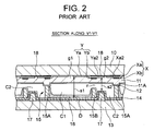
- Fig. 2 is a figure showing a section along V1-V1 in the display panel shown in Fig. 1 (see Fig. 2 in Patent Document 1).
- each discharge cell is constructed by a display cell C1 for causing sustain discharge only, and a reset-and-address discharge cell C2 for causing reset and address discharge with luminescence not to be involved in displaying an image.
- the display cell C1 and the reset-and-address discharge cell C2 have respective discharge spaces that are in communication through a gap r as shown in Fig. 2.
- the address discharge caused within the reset-and-address discharge cell C2 is extended toward the display cell C1 through the gap r. This places the display cell C1 in any one of an on-wall charge formed state allowing for sustain discharge under application of a sustain pulse (on mode) and an on-wall charge formed state not allowing for sustain discharge (off mode).
- sustain discharge is caused only within the display cell C1 set in on mode under application of a sustain pulse.
- the light caused by discharge is radiated to the outside through the front glass substrate 10, as shown in Fig. 2.
- a light-absorbing layer 18 in black or dark color shown in Fig. 2 is formed in order to block off the light caused by reset and address discharge from radiating to the outside.
- the light-absorbing layer 18 the light caused by reset and address discharge can be reduced in leak amount toward the display surface, hence improving the contrast of display image.
- the present invention has been made in order to solve the problem, and it is an object thereof to provide a display device capable of stabilizing discharge and improving luminescent efficiency.
- a display apparatus for displaying an image by causing luminescence on pixels in each of a plurality of sub-fields forming a field according to pixel-based pixel data on a basis of an input video signal
- the display apparatus comprises a display panel having front and back substrate oppositely arranged sandwiching a discharge space, a plurality of row electrode pairs covered with a dielectric layer and arranged on an inner surface of the front substrate, and a plurality of address electrodes arranged crossing the electrode pairs, wherein the electrode pairs and the address electrodes have intersections each formed with a unit luminescent region having a first discharge cell and a second discharge cell having a light absorbing layer provided on the front substrate side; an addressing unit for applying, while applying a scanning pulse sequentially to one electrodes of the row electrode pairs, a pixel data pulse corresponding to the pixel data to column electrodes simultaneously with the scanning pulse, in an address period of each of the sub-fields thereby causing address discharge within the second discharge cell; and a sustain unit
- At least one of the sustain pulses to be applied in the later section in a sustain period for which sustain pulses are to be repeatedly applied has a pulse voltage amplitude given greater than a pulse voltage amplitude of the other sustain pulse.
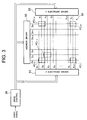
- Fig. 3 is a diagram showing an arrangement of a plasma display device as a display device according to the present invention.
- the plasma display device includes a PDP 50 as a plasma display panel, an X-electrode driver 51, a Y-electrode driver 53, an address driver 55 and a drive control circuit 56.
- strip-formed column electrodes (address electrodes) D 1 - D m each extending in a vertical direction of the display screen.
- strip-formed row electrodes X 1 - X n+1 and Y 1 - Y n extending in a horizontal direction of the display screen alternately and in an numbered order, as shown in Fig. 3.
- the pairs of adjacent row electrodes (Y 1 , X 2 ), (Y 2 , X 3 ), (Y 3 , X 4 ), ..., (Y n , X n+1 ) respectively serve for the first to n-th display lines of the PDP 50.
- Cells serving as pixels are formed respectively at the intersections of the display lines and the column electrodes D 1 - D m (regions of the one-dot chain line in Fig. 3). Namely, on the PDP 50, there is an arrangement in a matrix form of pixel cells PC 1,1 - PC 1,m belonging to the first display line, pixel cells PC 2,1 - PC 2,m belonging to the second display line, ... and pixel cells PC n,1 - PC n,m belonging to the n-th display line.
- Figs. 4 to 7 are views showing part, by excerption, of an internal structure of the PDP 50.
- Fig. 4 is a plan view as viewed from the display surface side.
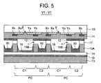
- Fig. 5 is a sectional view as viewed from line V1 - V1 shown in Fig. 4.
- Fig. 6 is a sectional view as viewed from line V2 - V2 shown in Fig. 4.
- Fig. 7 is a sectional view as viewed from line W1 - W12 shown in Fig. 4.
- the row electrode Y is constituted by a bus electrode Yb (main body portion of the row electrode Y) in a strip form extending in the horizontal (row) direction of the display screen and a plurality of transparent electrodes Ya connected to the bus electrode Yb.
- the bus electrode Yb is formed by a black metal film, for example.
- the transparent electrodes Ya are formed by a transparent conductive film such as of ITO, and arranged on the bus electrode Yb respectively in positions corresponding to the column electrodes D.
- the transparent electrode Ya extends in a direction orthogonal to the bus electrode Yb, whose one and the other ends are each made in a widened form as shown in Fig. 4.
- the transparent electrode Ya can be grasped as a projection electrode projecting from the main body portion of the row electrode Y.
- the row electrode X is constituted by a bus electrode Xb (main body portion of the row electrode X) in a strip form extending in the horizontal (row) direction of the display screen and a plurality of transparent electrodes Xa connected to the bus electrode Xb.
- the bus electrode Xb is formed by a black metal film, for example.
- the transparent electrodes Xa are formed by a transparent conductive film such as of ITO, and arranged on the bus electrode Xb respectively in positions corresponding to the column electrodes D.
- the transparent electrode Xa extends in a direction orthogonal to the bus electrode Xb, whose one and the other end are made in a widened form as shown in Fig. 4.
- the transparent electrode Xa can be understood as a projection electrode projecting from the main body of the row electrode X.
- the widened portions of the transparent electrodes Xa and Yb are arranged oppositely to each other through a predetermined width of discharge gap g, as shown in Fig. 4.
- the transparent electrodes Xa and Ya as projection electrodes projecting from the main bodies of the paired row electrodes X and Y, are oppositely arranged to each other through the discharge gap g.
- the row electrodes Y comprised of the transparent electrodes Ya and bus electrodes Yb and the row electrodes X, comprised of the transparent electrodes Xa and bus electrodes Xb, are formed on a backside of a front transparent substrate 10 serving as a display surface of the PDP 50, as shown in Fig. 5. Furthermore, a dielectric layer 11 is formed on a back surface of the front transparent substrate 10, to cover over those row electrodes X and Y. On the surface of the dielectric layer 11, a protruding dielectric layer 12 is formed protruding from the dielectric layer 11 toward the backside, in a position corresponding to each select cell C2 (referred later).
- the protruding dielectric layer 12 is formed by a strip-formed light-absorbing layer containing a black or dark-color pigment, to extend in a horizontal (row) direction of the display surface as shown in Fig. 4.
- the protruding dielectric layer 12 and the dielectric layer 11 free of the protruding dielectric layer 12 have their surfaces covered with a not-shown protection layer of MgO.
- a plurality of column electrodes D are arranged in parallel one with another through a predetermined gap and extending in a direction orthogonal to the bus electrodes Xb and Yb (in a column direction).
- a column-electrode protection layer (dielectric layer) 14 in white is formed covering over the column electrodes D.
- a barrier wall 15 is formed comprising a first horizontal wall 15A, a second horizontal wall 15B and a vertical wall 15C.
- the first horizontal wall 15A is formed extending in the horizontal direction of the display surface, in a position on the column-electrode protection layer 14 opposed to the bus electrode Yb.
- the second horizontal wall 15B is formed extending in the horizontal (row) direction of the display surface, in a position on the column-electrode protection layer 14 opposed to the bus electrode Xb.
- the vertical wall 15C is formed extending in a direction orthogonal to the bus electrode Xb (Yb), in a position between the transparent electrodes Xa (Ya) arranged at an equal interval on the bus electrode Xb (Yb).
- a secondary-electron emitting material layer 30 is formed on the column electrode protection layer 14 in a region opposed to the protruding dielectric layer 12 (including side surfaces of the vertical wall 15C and the first and second horizontal walls 15A and 15B) .
- the secondary-electron emitting material layer 30 is a layer formed of a high- ⁇ material low in work function (e.g. 4.2 eV or lower) but high in so-called secondary electron emission coefficient.
- the secondary electron emitting material layer 30 employs a material, for example, of an alkali earth metal oxide such as MgO, CaO, SrO and BaO; an alkali metal oxide such as Cs 2 O; a fluoride such as CaF 2 and MgF 2 ; TiO 2 , Y 2 O; a material enhanced in secondary electron emission coefficient by crystal defect or impurity dope, or the like.
- a fluorescent layer 16 is formed on the column electrode protection layer 14 in the other region than the region opposed to the protruding dielectric layer 12 (including side surfaces of the vertical wall 15C and the first and second horizontal walls 15A and 15B) , as shown in Fig. 5.
- the fluorescent layer 16 includes three types of a red fluorescent layer for luminescence in red, a green fluorescent layer for luminescence in green and a blue fluorescent layer for luminescence in blue, which are fixedly assigned to the pixel cells PC.
- the first and second horizontal walls 15A, 15B and the vertical wall 15C are not so high as reaching a surface of the protruding dielectric layer 12 or dielectric layer 11, as shown in Figs. 5 and 7.
- a gap r exists between the second horizontal wall 15B and the protruding dielectric layer 12 as shown in Fig. 5, allowing for communication of the discharge gas.
- a dielectric layer 17 is formed extending in a direction along the first horizontal wall 15A in order to prevent against discharge gas interference.
- a dielectric layer 18 is formed intermittently in a direction along the vertical wall 15C, as shown in Fig. 6.
- the region surrounded by the first horizontal wall 15A and the vertical wall 15C (the region shown by the one-dot chain line in Fig. 4) is given as a pixel cell PC serving as a pixel.
- the pixel cell PC is divided into a display discharge cell C1 and a selection discharge cell C2 by the second horizontal wall 15B.
- the display discharge cell C1 includes transparent electrodes Xa and Ya of a pair of row electrodes X and Y serving as a display line and a fluorescent layer 16, as shown in Figs. 4 and 5.
- the selection discharge cell C2 includes a protruding dielectric layer 12, a second electron emission material layer 30, a row electrode Y of a pair of row electrodes corresponding to a display line, and a bus electrode Xb of a row electrode X of an electrode pair corresponding to the adjacent display line above the relevant display line.
- the discharge gap g provided between the broadened portion of the transparent electrode Xa and the broadened portion of the transparent electrode Xb, lies at an intermediate position between the bus electrode Xb and the bus electrode Yb within the display discharge cell C1.
- the respective discharge spaces of the adjacent pixel cells PC that are adjacent to each other with respect to the vertical direction (left-right direction in Fig. 5) of the display surface are blocked by the first horizontal wall 15A and dielectric layer 17. Nevertheless, the respective discharge spaces of the display discharge cell C1 and the selection discharge cell C2 that belong to the same pixel cell PC are in communication through a gap r, as shown in Fig. 5. Furthermore, the respective discharge spaces of the mutually adjacent select cells C2 with respect to the left-right direction of the display surface are blocked by the protruding dielectric layer 12 and dielectric layer 18, as shown in Fig. 6. However, the respective discharge spaces of the mutually adjacent display cells C1 with respect to the left-right direction of the display surface are in communication with each other.
- the pixel cells PC 1,1 - PC n,m formed in the PDP 50 are each structured with a display discharge cell C1 and a selection discharge cell C2 which have the respective discharge spaces communicating with each other.
- the X electrode driver 51 applies various pulses (described later) to the row electrodes X 1 - X n+1 of the PDP 50, according to a timing signal supplied from the drive control circuit 56.
- the Y electrode driver 53 applies various pulses (referred later) to the row electrodes Y 1 - Y n of the PDP 50, according to a timing signal supplied from the drive control circuit 56.
- the address driver 55 applies a pixel data pulse (described later) to the column electrodes D 1 - D m of PDP 50, according to a timing signal supplied from the drive control circuit 56.
- the drive control circuit 56 first converts the input video signal into, for example, 8-bit pixel data representing a luminance level on each pixel and carries out an error diffusion process and dither process on the pixel data. For example, in the error diffusion process, firstly the higher 6 bits of the pixel data is taken as display data and the remaining lower 2 bits as error data. The error data of the image data corresponding to each peripheral pixel is summed up by weighting into reflection in the display data. By this operation, the luminance in an amount of the lower 2 bits of the original pixel is expressed by the peripheral pixels in a pseudo-representation fashion. Therefore, by use of display data in an amount of 6 bits less than 8 bits, luminance tonal expression is made feasible equivalent to the pixel data in an amount of 8 bits.
- Dither process is carried out on 6-bit error-diffused pixel data obtained by the error diffusion process.
- a plurality of mutually adjacent pixels are taken as one pixel unit.
- the error diffused pixel data corresponding to each pixel of the one pixel unit are added by respectively assigning dither coefficients different in value, thereby obtaining dither addition pixel data.
- dither coefficient addition it is possible to express a luminance corresponding to 8 bits by use of the higher 4 bits only of the dither addition pixel data as seen on the 1-pixel unit basis. For this reason, the drive control circuit 56 extracts the higher 4 bits of dither addition pixel data as multi-toned or multi-gradation pixel data PDs.
- the drive control circuit 56 separates the pixel drive data GD 1,1 - GD n,m at the same bit place, based on pixel drive data GD 1,1 - GD n,m corresponding respectively to the pixel cells PC 1,1 - PC n,m , thereby obtaining pixel drive data bit group DB1 - DB15 as follows.
- pixel drive data bit groups DB1 - DB15 respectively correspond to sub-fields SF1 - SF15, described later.
- the drive control circuit 56 in each of fifteen sub-fields SF1 - SF15 constituting the fields of a video signal, carries out a drive control based on an address period W and a sustain period I (referred later) onto the X electrode driver 51, the Y electrode driver 53 and the address driver 55, as shown in Fig. 9.
- the drive control circuit 56 in the address period W in each of sub-fields SF1 - SF15, supplies a pixel drive data bit group DB corresponding to the relevant sub-field SF in an amount of one display line (m in the number) per time to the address driver 55.
- the drive control circuit 56 only in the starting sub-field SF1, carries out drive control based on a reset period R (referred later) in advance of the address period W and, only in the last sub-field SF15, carries out drive control based on an erase period E (referred later) immediately after the sustain period I.
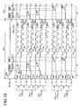
- Fig. 10 is a figure showing various drive pulses which the X electrode driver 51, the Y electrode driver 53 and the address driver 55 are to apply to the PDP 50 in accordance with carrying out of the above drive control.
- Fig. 10 shows, by excerption, only the starting sub-field SF1 of the sub-fields SF1 - SF15 shown in Fig. 9.
- the X electrode driver 51 At first, in the reset period R, the X electrode driver 51 generates a reset pulse RP X in positive polarity and applies it simultaneously to the row electrodes X 1 - X n+1 of the PDP 50.
- the Y electrode driver 53 During application of the reset pulse RP X , as shown in Fig. 10 the Y electrode driver 53 generates a reset pulse RP Y moderate in fall change and in negative polarity and applies it simultaneously to the row electrodes Y 1 - Y n of the PDP 50.
- the address driver 55 In this duration, the address driver 55 generates a reset pulse RP D in positive polarity and applies it simultaneously to the column electrodes D 1 - D m .
- reset discharge (write discharge) is caused at between the column electrode D and the row electrode Y within the selection discharge cell C2 of every pixel cell PC of the PDP 50.
- On-wall charge is formed within the selection discharge cell C2.
- the column electrodes D is placed as an anode relative to the row electrodes X and Y.
- the reset discharge moves toward the display discharge cell C1 through the gap r shown in Fig. 5, to cause discharge at between the electrodes Y and X within the display discharge cell C1.
- on-wall charge is formed within the display discharge cell C1 of every pixel cell PC.
- the Y electrode driver 53 applies a scanning pulse SP having a positive-polarity voltage V2 (V2 > V1) sequentially to the row electrodes Y 1 - Y n , while applying a positive-polarity voltage V1 to all the row electrodes Y 1 - Y n .
- the X electrode driver 51 places the row electrodes X 1 - X n+1 at 0V.
- the address driver 55 converts each data bit of the pixel drive data bit group DB corresponding to the sub-field SF into a pixel data pulse DP having a pulse voltage corresponding to a logical level thereof.
- the address driver 55 converts a pixel drive data bit having a logical level 0 into a pixel data pulse DP positive in polarity and high in voltage and, on the other hand, converts a pixel drive data bit having a logical level 1 into a pixel data pulse DP low in voltage (0 volt).
- Such pixel data pulses DP are applied in an amount of one display line (m in the number) per time to the column electrodes D 1 - D m , in synchronism with the application timing of the scanning pulse SP.
- the address driver 55 first applies a pixel data pulse group DP 1 comprising pixel data pulses DP in the number of m corresponding to the first display line to the column electrodes D 1 - D m , and then applies a pixel data pulse group DP 2 comprising pixel data pulses DP in the number of m corresponding to the second display line to the column electrodes D 1 - D m .
- erase address discharge is caused at between the row electrode D and the row electrode Y within the selection discharge cell C2 of the pixel cell PC to which the scanning pulse SP having a positive-polarity voltage V2 and the pixel data pulse DP having a low voltage (0 volt) are applied at the same time.
- the on-wall charge within the display discharge cell C1 maintains its formation state as it is. Namely, where on-wall charge exists within the display discharge cell C1, it remains as it is. Where it does not exist, the non-formation state of on-wall charge is maintained.
- erase address discharge is selectively caused within the selection discharge cell C2 of the pixel cell PC according to the data bit of a pixel drive data bit group corresponding to the sub-field, thereby erasing the on-wall charge.
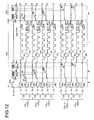
- the X electrode driver 51 repeatedly applies a negative-polarity sustain pulse IP X to the row electrodes X 1 - X n+1 while the Y electrode driver 53 repeatedly applies a negative-polarity sustain pulse IP Y to the row electrodes Y 1 - Y n .
- the sustain pulse IP YE to be applied the last within the sustain period I has a pulse-voltage amplitude V S2 approximately 10 - 50 volts greater than a pulse-voltage amplitude V S1 of the sustain pulse IP Y and IP X to be applied up to immediately before that time.
- sustain pulses IP X and IP Y are applied the number of times assigned to the sub-field to which the relevant sustain period I belongs.
- a sustain pulse IP X or IP Y (including IP YE ) is applied, sustain discharge is caused at between the transparent electrodes Xa and Ya within the display discharge cell C1 of the pixel cell PC set in the on-cell mode. Due to a ultraviolet ray caused by such sustain discharge, as shown in Fig. 5 there is caused excitation in the fluorescent layer 16 (red fluorescent layer, green fluorescent layer and blue fluorescent layer) formed within the display discharge cell C1, to cause a radiation corresponding to the fluorescent color through the front transparent substrate 10.
- the fluorescent layer 16 red fluorescent layer, green fluorescent layer and blue fluorescent layer
- luminescence is repeatedly caused based on sustain discharge the number of times assigned to the sub-field to which the sustain period I belongs.
- Visual perception is obtained at a luminescence commensurate with the number of times.
- erase address discharge is caused only within the address period W of one of sub-fields SF1 - SF15 (shown by solid circle), to set the pixel cell PC into an off-cell mode.
- luminescence is repeatedly caused based on sustain discharge by the number of times assigned to the sub-field in a duration of from a setting to an on-cell mode in the reset period R of the starting sub-field SF1 to a setting to an off-cell mode in the address period W of any one of sub-fields SF1 - SF15 (shown by open circle).
- visual perception is obtained at a luminance corresponding to the total number of luminescence based on sustain discharge caused within one sub-field. Consequently, according to the 16 luminescent patterns based on first to sixteenth tonal levels driving as shown in Fig. 8, expression is obtained at a halfway intensity in 16 levels corresponding to the total number of times of sustain discharge caused in the sub-fields shown by the open circles.
- the sustain pulse IP Y and IP X has a pulse-voltage amplitude V S1 set at a comparatively small amplitude for the charged particle not to extend toward the selection discharge cell C2 due to the sustain discharge caused by application of the sustain pulse. Accordingly, because there is eliminated of flowing out of the charged particle formed within the discharge space of the display discharge cell C1 due to sustain discharge, luminescent efficiency can be improved.
- the dielectric layer 11 can be suppressed from deteriorating due to sustain discharge, thus enabling to increase the life of the PDP 50.
- the amplitude V S2 of the sustain pulse IP YE to be applied the last in the sustain period I is increased to such an extent that the charged particle formed by sustain discharge can be extended toward the selection discharge cell C2 through the gap r as shown in Fig. 5. Accordingly, because the charged particle remains in the discharge space of the selection discharge cell C2 immediately before the address period W of the next sub-field SF, address discharge can be stably caused in the address period W.
- the sustain pulse IP YE to be applied the last in the sustain period I is given a pulse voltage amplitude V S2 greater than the amplitude V S1 of the sustain pulse IP Y to be applied up to immediately before that time.
- V S2 the pulse voltage amplitude V S2
- the sustain pulse IP YE to be applied the last in the sustain period I may be given a pulse voltage amplitude V S1 while the sustain pulse IP Y to be applied immediately before the sustain pulse IP YE may be given a pulse voltage amplitude V S2 greater than the amplitude V S1 .
- the sustain pulse IP YE to be applied the last in the sustain period I and the sustain pulse IP Y to be applied immediately before that time may be given a pulse voltage amplitude of V S2 ⁇
- the embodiment shown in Figs. 10 - 11 adopts the driving that the column electrode D is relatively taken as a negative polarity to thereby cause reset and address discharge so that a negative-polarity sustain pulse can be applied to cause sustain discharge
- the polarity may be inverted during driving. Namely, the column electrode D may be relatively taken as a positive polarity side to thereby cause reset and address discharge so that a positive-polarity sustain pulse IP can be applied to cause sustain discharge.
- such an arrangement as X-Y, X-Y, X-Y, X-Y is adopted as an arrangement of row electrode pairs corresponding respectively to the first to n-th display lines of PDP50.
- the arrangement may be like X-Y, Y-X, X-Y, Y-X.
- placed adjacent mutually are a selection discharge cell C2 within the pixel cell PC belonging to the odd line and a selection discharge cell C2 within the pixel cell PC belonging to the even line.
Landscapes
- Engineering & Computer Science (AREA)
- Physics & Mathematics (AREA)
- Computer Hardware Design (AREA)
- General Physics & Mathematics (AREA)
- Theoretical Computer Science (AREA)
- Plasma & Fusion (AREA)
- Power Engineering (AREA)
- Control Of Indicators Other Than Cathode Ray Tubes (AREA)
- Gas-Filled Discharge Tubes (AREA)
- Transforming Electric Information Into Light Information (AREA)
- Control Of Gas Discharge Display Tubes (AREA)
Applications Claiming Priority (2)
| Application Number | Priority Date | Filing Date | Title |
|---|---|---|---|
| JP2003356698A JP2005121905A (ja) | 2003-10-16 | 2003-10-16 | 表示装置 |
| JP2003356698 | 2003-10-16 |
Publications (2)
| Publication Number | Publication Date |
|---|---|
| EP1524642A2 true EP1524642A2 (de) | 2005-04-20 |
| EP1524642A3 EP1524642A3 (de) | 2005-06-22 |
Family
ID=34373608
Family Applications (1)
| Application Number | Title | Priority Date | Filing Date |
|---|---|---|---|
| EP04023948A Withdrawn EP1524642A3 (de) | 2003-10-16 | 2004-10-07 | Anzeigevorrichtung |
Country Status (5)
| Country | Link |
|---|---|
| US (1) | US20050083256A1 (de) |
| EP (1) | EP1524642A3 (de) |
| JP (1) | JP2005121905A (de) |
| KR (1) | KR20050036823A (de) |
| CN (1) | CN1609928A (de) |
Families Citing this family (4)
| Publication number | Priority date | Publication date | Assignee | Title |
|---|---|---|---|---|
| KR100637508B1 (ko) * | 2004-11-30 | 2006-10-23 | 삼성에스디아이 주식회사 | 플라즈마 표시 장치 및 플라즈마 표시 패널의 구동 방법 |
| US8165909B2 (en) * | 2005-05-17 | 2012-04-24 | The United States Postal Service | System and method for automated management of an address database |
| KR100684735B1 (ko) * | 2005-10-12 | 2007-02-20 | 삼성에스디아이 주식회사 | 플라즈마 표시 장치 및 그 구동 방법 |
| CN100501820C (zh) * | 2005-11-01 | 2009-06-17 | 中华映管股份有限公司 | 利用多放电现象以提高等离子显示面板特性之驱动方法与装置 |
Family Cites Families (19)
| Publication number | Priority date | Publication date | Assignee | Title |
|---|---|---|---|---|
| US4638218A (en) * | 1983-08-24 | 1987-01-20 | Fujitsu Limited | Gas discharge panel and method for driving the same |
| JP3891499B2 (ja) * | 1995-04-14 | 2007-03-14 | パイオニア株式会社 | プラズマディスプレイパネルにおける輝度調整装置 |
| JP3544763B2 (ja) * | 1995-11-15 | 2004-07-21 | 株式会社日立製作所 | プラズマディスプレイパネルの駆動方式 |
| JP2907167B2 (ja) * | 1996-12-19 | 1999-06-21 | 日本電気株式会社 | カラープラズマディスプレイパネル |
| US6020687A (en) * | 1997-03-18 | 2000-02-01 | Fujitsu Limited | Method for driving a plasma display panel |
| JP2994631B2 (ja) * | 1997-12-10 | 1999-12-27 | 松下電器産業株式会社 | Pdp表示の駆動パルス制御装置 |
| JP3556097B2 (ja) * | 1998-06-30 | 2004-08-18 | 富士通株式会社 | プラズマディスプレイパネル駆動方法 |
| JP2000089720A (ja) * | 1998-09-10 | 2000-03-31 | Fujitsu Ltd | プラズマディスプレイの駆動方法及びプラズマディスプレイ装置 |
| KR100374100B1 (ko) * | 1998-09-11 | 2003-04-21 | 엘지전자 주식회사 | 플라즈마표시패널의구동방법 |
| JP3266191B2 (ja) * | 1998-12-25 | 2002-03-18 | 日本電気株式会社 | プラズマ・ディスプレイ、その画像表示方法 |
| EP1020838A1 (de) * | 1998-12-25 | 2000-07-19 | Pioneer Corporation | Verfahren zur Ansteuerung einer Plasmaanzeigetafel |
| EP1233395A4 (de) * | 1999-10-19 | 2008-11-19 | Helligkeitsabstufungsverfahren mit wirksamer reduzierung des flimmerns und anzeige mit helligkeitsabstufung | |
| JP2001228823A (ja) * | 1999-12-07 | 2001-08-24 | Pioneer Electronic Corp | プラズマディスプレイ装置 |
| JP2001234163A (ja) * | 2000-02-25 | 2001-08-28 | Sony Corp | 発光性結晶粒子、発光性結晶粒子組成物、表示用パネル及び平面型表示装置 |
| JP2003005701A (ja) * | 2001-06-20 | 2003-01-08 | Pioneer Electronic Corp | プラズマディスプレイパネルの駆動方法 |
| TW589602B (en) * | 2001-09-14 | 2004-06-01 | Pioneer Corp | Display device and method of driving display panel |
| JP2003131615A (ja) * | 2001-10-30 | 2003-05-09 | Sharp Corp | プラズマディスプレイ装置及びその駆動方法 |
| JP4308488B2 (ja) * | 2002-03-12 | 2009-08-05 | 日立プラズマディスプレイ株式会社 | プラズマディスプレイ装置 |
| JP2004029553A (ja) * | 2002-06-27 | 2004-01-29 | Pioneer Electronic Corp | 表示パネルの駆動装置 |
-
2003
- 2003-10-16 JP JP2003356698A patent/JP2005121905A/ja not_active Abandoned
-
2004
- 2004-10-07 US US10/959,220 patent/US20050083256A1/en not_active Abandoned
- 2004-10-07 EP EP04023948A patent/EP1524642A3/de not_active Withdrawn
- 2004-10-15 KR KR1020040082809A patent/KR20050036823A/ko not_active Abandoned
- 2004-10-15 CN CNA2004100841183A patent/CN1609928A/zh active Pending
Also Published As
| Publication number | Publication date |
|---|---|
| US20050083256A1 (en) | 2005-04-21 |
| KR20050036823A (ko) | 2005-04-20 |
| JP2005121905A (ja) | 2005-05-12 |
| CN1609928A (zh) | 2005-04-27 |
| EP1524642A3 (de) | 2005-06-22 |
Similar Documents
| Publication | Publication Date | Title |
|---|---|---|
| EP1381016A2 (de) | Verfahren und Einrichtung zum Steuern einer Plasmaanzeigetafel | |
| CN100382126C (zh) | 等离子体显示面板的驱动方法 | |
| KR100529203B1 (ko) | 표시 장치 및 표시 패널 구동 방법 | |
| KR100661146B1 (ko) | 복수의 방전 셀을 단위 발광 영역에 갖는 표시 장치 | |
| KR100703104B1 (ko) | 표시 장치 | |
| EP1524642A2 (de) | Anzeigevorrichtung | |
| KR100643747B1 (ko) | 표시장치 및 표시패널의 구동방법 | |
| US7136034B2 (en) | Method of driving a display panel | |
| EP1406237A2 (de) | Plasma-Anzeigetafel mit doppelten Entladungszellen und Verfahren zu ihrer Ansteuerung | |
| US20060022902A1 (en) | Display device | |
| US7391392B2 (en) | Method and device for driving display panel unit | |
| WO2004077485A1 (ja) | プラズマディスプレイパネル及び表示装置 | |
| JP2006171400A (ja) | 表示装置 | |
| JP2008015237A (ja) | 表示装置 | |
| JP2008026360A (ja) | 表示パネルの駆動方法 | |
| JP2007334117A (ja) | 表示装置 | |
| JP2006003792A (ja) | 表示装置及び表示パネルの駆動方法 | |
| JP2007316297A (ja) | 表示装置及び表示パネルの駆動方法 | |
| JP2008003213A (ja) | 表示パネルの駆動方法 | |
| JP2008003470A (ja) | 表示パネルの駆動方法 | |
| JP2006162844A (ja) | 表示装置 | |
| JP2008003471A (ja) | 表示パネルの駆動方法 |
Legal Events
| Date | Code | Title | Description |
|---|---|---|---|
| PUAI | Public reference made under article 153(3) epc to a published international application that has entered the european phase |
Free format text: ORIGINAL CODE: 0009012 |
|
| AK | Designated contracting states |
Kind code of ref document: A2 Designated state(s): AT BE BG CH CY CZ DE DK EE ES FI FR GB GR HU IE IT LI LU MC NL PL PT RO SE SI SK TR |
|
| AX | Request for extension of the european patent |
Extension state: AL HR LT LV MK |
|
| PUAL | Search report despatched |
Free format text: ORIGINAL CODE: 0009013 |
|
| AK | Designated contracting states |
Kind code of ref document: A3 Designated state(s): AT BE BG CH CY CZ DE DK EE ES FI FR GB GR HU IE IT LI LU MC NL PL PT RO SE SI SK TR |
|
| AX | Request for extension of the european patent |
Extension state: AL HR LT LV MK |
|
| 17P | Request for examination filed |
Effective date: 20050607 |
|
| AKX | Designation fees paid |
Designated state(s): DE FR GB |
|
| STAA | Information on the status of an ep patent application or granted ep patent |
Free format text: STATUS: THE APPLICATION IS DEEMED TO BE WITHDRAWN |
|
| 18D | Application deemed to be withdrawn |
Effective date: 20080418 |