EP1517366A2 - Procédé de fabrication des tranchées avec un profil de profondeur dual - Google Patents
Procédé de fabrication des tranchées avec un profil de profondeur dual Download PDFInfo
- Publication number
- EP1517366A2 EP1517366A2 EP04104237A EP04104237A EP1517366A2 EP 1517366 A2 EP1517366 A2 EP 1517366A2 EP 04104237 A EP04104237 A EP 04104237A EP 04104237 A EP04104237 A EP 04104237A EP 1517366 A2 EP1517366 A2 EP 1517366A2
- Authority
- EP
- European Patent Office
- Prior art keywords
- trench
- copper
- vias
- edge
- layer
- Prior art date
- Legal status (The legal status is an assumption and is not a legal conclusion. Google has not performed a legal analysis and makes no representation as to the accuracy of the status listed.)
- Withdrawn
Links
Images


Classifications
-
- H—ELECTRICITY
- H10—SEMICONDUCTOR DEVICES; ELECTRIC SOLID-STATE DEVICES NOT OTHERWISE PROVIDED FOR
- H10W—GENERIC PACKAGES, INTERCONNECTIONS, CONNECTORS OR OTHER CONSTRUCTIONAL DETAILS OF DEVICES COVERED BY CLASS H10
- H10W20/00—Interconnections in chips, wafers or substrates
- H10W20/01—Manufacture or treatment
- H10W20/071—Manufacture or treatment of dielectric parts thereof
- H10W20/081—Manufacture or treatment of dielectric parts thereof by forming openings in the dielectric parts
- H10W20/084—Manufacture or treatment of dielectric parts thereof by forming openings in the dielectric parts for dual-damascene structures
- H10W20/085—Manufacture or treatment of dielectric parts thereof by forming openings in the dielectric parts for dual-damascene structures involving intermediate temporary filling with material
Definitions
- the invention is generally related to the field of integrated circuits and more specifically to a dual trench depth termination method for improving the integrity of Cu-based semiconductor interconnects.
- High performance integrated circuits utilize low K dielectric layers and copper metal to form the lines that interconnect the various electronic devices that comprise the circuit.
- the copper interconnect lines comprise copper formed in trenches and vias in the low K dielectric material.
- FIG. 1 Illustrated in Figure 1 is a cross section diagram of a typical copper interconnect structure showing copper delamination. Copper delamination is a major problem that affects the reliability and operation of the integrated circuit.
- a dielectric layer 10 is formed over a semiconductor. Electronic devices such as transistors, capacitors, and diodes will be formed in the semiconductor. In addition there may be any number of intervening layers and structures between the semiconductor and the dielectric layer 10. The semiconductor and any intervening layers have been omitted for clarity.
- a copper layer 20 is formed in the dielectric layer using known methods.
- a barrier layer 30 is formed on the copper layer and a second dielectric layer 40 is formed over the barrier layer.
- a dielectric layer is formed over a semiconductor. Any number of intervening layers can be formed between the semiconductor and the dielectric layer.
- a plurality of vias, separated by a minimum distance X v is formed in the dielectric layer to allow the subsequently formed copper layer to contact an underlying copper layer.
- a trench is formed in the dielectric layer over the plurality of vias with an edge that extends a minimum distance of X TO from the edge ⁇ of the via closest to the edge of the trench.
- the trench can comprise a depth d 1 in the region containing the vias and a depth d 2 at the edge of the trench. In general the condition d 1 > d 2 will apply to the depths of the trench.
- the trench and vias will be filled with copper to form a copper interconnect line. The minimum overhang of the copper line will reduce and/or eliminate the copper delamination the currently occurs.
- a copper metal layer 20 is formed on a dielectric layer 10.
- the dielectric layer 10 is formed over a semiconductor. Electronic devices such as transistors, capacitors, and diodes will be formed in the semiconductor. In addition there may be any number of intervening layers and structures between the semiconductor and the dielectric layer 10. The semiconductor and any intervening layers have been omitted for clarity.
- a barrier layer 30 is formed on the copper layer 20. This barrier layer can comprise silicon nitride or any other suitable dielectric material.
- a dielectric layer 100 is formed on the barrier layer.
- the dielectric layer 100 can comprise a low dielectric constant (herein after low K dielectric) material.
- low K refers to dielectric material with a dielectric constant of 3.8 and below. This should be compared with silicon oxide that has a dielectric constant of 3.9.
- Some examples of low K dielectrics that can be used to form the dielectric layer 100 are fluorine-doped silicate glass (FSG), silsesquioxanes, and organosilicate glass (OSG).
- OSG material can be formed by chemical vapor deposition (CVD) using organosilane precursors or spin-on using silsesquioxanes.
- low K material that can be used to form layer 100 include, but is not limited to, poly(arylene ether), parylene, fluoro-polymer, fluorinated amorphous carbon, diamondlike carbon, porous silica, mesoporous silica, porous silsesquioxane, porous polyimide, and porous poly(arylene ether).
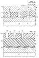
- a patterned photoresist layer 110 is formed on the dielectric layer to define a pattern for the etching of the vias 120.
- FIG. 2(b) Shown in Figure 2(b) is the dielectric structure of Figure 2 (a) following the etching of the vias 120 in the dielectric layer 100.
- a material 130 is used to fill the vias 120.
- the material 130 that is used is the same material used to form the backside antireflective coating (BARC) layer.
- BARC backside antireflective coating
- many different types of organic and inorganic material can be used to fill the via.
- a second patterned photoresist layer comprising 140 and 140a is formed on the dielectric layer to define the trench. The portion of the patterned photoresist layer 140a is optional.
- the trench structure is formed in the dielectric layer using a dry etching method.
- dry etching refers to an etch process the does not use liquid chemical etching but instead comprises a plasma assisted etching process.
- FIG. 2(c) Shown in Figure 2(c) is the structure of Figure 2(b) following the etching of the trench in the dielectric layer 100.
- the portion of the patterned resist layer 140a was not present or was removed during the trench etching process.
- a dual depth trench structure is formed. The depth of the trench is measured from the surface of the dielectric layer 100. The first trench depth is d 1 and the second trench depth is d 2 where d 1 > d 2 .
- the region of the trench R 1 that comprises the vias 120 is substantially at the depth d 1 .
- There is a transition region R 2 where the depth of the trench transitions from d 1 to d 2 .
- the depth of this transition region is designated d 3 where d 2 ⁇ d 3 ⁇ d 1 .
- the third region R 3 represents the region of the trench where the trench depth is substantially d 2 .
- the vias are separated by a distance X v as shown in Figure 2(c).
- the separation X v of the vias 120 is less than 0.7um and there are n vias where n > 2.
- a minimum trench termination overhand X TO must be included.
- Such a minimum trench termination overhang X TO is shown in Figure 2(c) and is defined as the distance from the edge ⁇ of the via closest to the end of the trench to the end of the trench.
- the minimum trench termination overhang X TO is greater than 0.2um.
- the minimum trench termination overhang X TO is greater than 0.35um.
- the minimum trench termination overhang X TO is greater than 0.5um. It should be noted that the trench depth at the end of the trench need not necessarily be d 2 as shown in the Figure. It is intended that the instant invention encompass any trench depth from d 2 to d 1 .
- the remaining patterned photoresist layer 140 is removed and copper 150 and 160 is used to fill the vias and the trench respectively as shown in Figure 2(d).
- the copper structure that exists in the minimum trench overhand X TO will prevent the copper structure 150, 160 from delaminating from the underlying copper layer 20.
- a copper layer 150 comprising a plurality of n copper vias 160 (where n > 2) separated by distance X v must include a minimum termination copper structure (labeled T in Figure 2(d)) between the edge of the last via and the end of the copper layer.
- the length of the minimum copper termination structure is greater than X TO where X TO can be 0.2um, 0.35um, or 0.5um.
- the thickness of the copper layer that comprises the via structures 150 is t 1 and the thickness of the minimum termination copper structure T can be any value down to an including t 2 as shown in Figure 2(d).
- FIG. 2(e) Shown in Figure 2(e) is a cross section of the trench structure formed when the patterned photoresist structure 140a remains during the trench etching process.
- the resulting trench depth is substantially uniform at a depth d 4 .
- the vias are separated by a distance X v where X v is less than 1.0 ⁇ m and the number of vias n is greater than 2.
- a minimum trench termination overhand X TO must be included as shown in Figure 2(e). It is defined as the distance from the edge ⁇ of the via closest to the end of the trench to the end of the trench.
- the minimum trench termination overhang X TO is greater than 0.2um. In a further embodiment of the instant invention the minimum trench termination overhang X TO is greater than 0.35um. In yet a further embodiment of the instant invention the minimum trench termination overhang X TO is greater than 0.5um.
- the remaining patterned photoresist layer 140 is removed and copper 155 and 165 is used to fill the vias and the trench respectively as shown in Figure 2(f). The copper structure that exists in the minimum trench overhand X TO will prevent the copper structure 155, 165 from delaminating from the underlying copper layer 20.
- a copper layer 155 comprising a plurality of n copper vias 165 (where n > 2) separated by distance X v must include a minimum termination copper structure (labeled T in Figure 2(f)) between the edge ⁇ of the last via and the end of the copper layer.
- the length of the minimum copper termination structure is greater than X TO where X TO can be 0.2um, 0.35um, or 0.5um.
- the minimum copper termination structure at the end of a copper line in an integrated circuit is counter intuitive to the trend in integrated circuits to minimize the length of the copper lines used to form the circuit.
- the minimum termination copper structure reduces the stress (and in particular shear stress) existing at the end of the copper interconnect line. This reduction in stress will reduce the initiation of crack propagation that eventually leads to the delamination of the copper line. The delamination problem will become more severe as the dielectric constant of the material in which the copper line is formed is lowered.
Landscapes
- Internal Circuitry In Semiconductor Integrated Circuit Devices (AREA)
Applications Claiming Priority (2)
| Application Number | Priority Date | Filing Date | Title |
|---|---|---|---|
| US663948 | 2000-09-18 | ||
| US10/663,948 US7387960B2 (en) | 2003-09-16 | 2003-09-16 | Dual depth trench termination method for improving Cu-based interconnect integrity |
Publications (2)
| Publication Number | Publication Date |
|---|---|
| EP1517366A2 true EP1517366A2 (fr) | 2005-03-23 |
| EP1517366A3 EP1517366A3 (fr) | 2006-05-17 |
Family
ID=34194738
Family Applications (1)
| Application Number | Title | Priority Date | Filing Date |
|---|---|---|---|
| EP04104237A Withdrawn EP1517366A3 (fr) | 2003-09-16 | 2004-09-02 | Procédé de fabrication des tranchées avec un profil de profondeur dual |
Country Status (4)
| Country | Link |
|---|---|
| US (2) | US7387960B2 (fr) |
| EP (1) | EP1517366A3 (fr) |
| JP (1) | JP2005094008A (fr) |
| TW (1) | TW200522256A (fr) |
Families Citing this family (1)
| Publication number | Priority date | Publication date | Assignee | Title |
|---|---|---|---|---|
| US7781892B2 (en) * | 2005-12-22 | 2010-08-24 | Taiwan Semiconductor Manufacturing Company, Ltd. | Interconnect structure and method of fabricating same |
Family Cites Families (9)
| Publication number | Priority date | Publication date | Assignee | Title |
|---|---|---|---|---|
| US5670425A (en) * | 1995-11-09 | 1997-09-23 | Lsi Logic Corporation | Process for making integrated circuit structure comprising local area interconnects formed over semiconductor substrate by selective deposition on seed layer in patterned trench |
| JP4094174B2 (ja) * | 1999-06-04 | 2008-06-04 | 株式会社ルネサステクノロジ | 半導体装置の製造方法 |
| JP3574383B2 (ja) * | 2000-07-31 | 2004-10-06 | 富士通株式会社 | 半導体装置及びその製造方法 |
| US6468894B1 (en) * | 2001-03-21 | 2002-10-22 | Advanced Micro Devices, Inc. | Metal interconnection structure with dummy vias |
| US6566242B1 (en) * | 2001-03-23 | 2003-05-20 | International Business Machines Corporation | Dual damascene copper interconnect to a damascene tungsten wiring level |
| US6798073B2 (en) * | 2001-12-13 | 2004-09-28 | Megic Corporation | Chip structure and process for forming the same |
| JP3790469B2 (ja) | 2001-12-21 | 2006-06-28 | 富士通株式会社 | 半導体装置 |
| US6734090B2 (en) * | 2002-02-20 | 2004-05-11 | International Business Machines Corporation | Method of making an edge seal for a semiconductor device |
| JP4250006B2 (ja) * | 2002-06-06 | 2009-04-08 | 富士通マイクロエレクトロニクス株式会社 | 半導体装置及びその製造方法 |
-
2003
- 2003-09-16 US US10/663,948 patent/US7387960B2/en not_active Expired - Lifetime
-
2004
- 2004-08-31 TW TW093126285A patent/TW200522256A/zh unknown
- 2004-09-02 EP EP04104237A patent/EP1517366A3/fr not_active Withdrawn
- 2004-09-15 JP JP2004267709A patent/JP2005094008A/ja active Pending
-
2008
- 2008-05-12 US US12/119,187 patent/US20090121358A1/en not_active Abandoned
Also Published As
| Publication number | Publication date |
|---|---|
| TW200522256A (en) | 2005-07-01 |
| JP2005094008A (ja) | 2005-04-07 |
| US20050059189A1 (en) | 2005-03-17 |
| US20090121358A1 (en) | 2009-05-14 |
| EP1517366A3 (fr) | 2006-05-17 |
| US7387960B2 (en) | 2008-06-17 |
Similar Documents
| Publication | Publication Date | Title |
|---|---|---|
| CN100463164C (zh) | 半导体结构及其形成方法 | |
| US7871923B2 (en) | Self-aligned air-gap in interconnect structures | |
| TWI232481B (en) | Manufacturing method for semiconductor device and the semiconductor device | |
| CN101958247A (zh) | 半导体器件处理方法 | |
| US20020106889A1 (en) | Slot via filled dual damascene structure without middle stop layer and method for making the same | |
| JP2004179659A (ja) | 集積回路におけるダマシン金属導体のためのビア形成 | |
| KR20010019643A (ko) | 저유전율 절연막을 갖는 다층 금속배선의 형성방법 | |
| US6821896B1 (en) | Method to eliminate via poison effect | |
| US6984875B2 (en) | Semiconductor device with improved reliability and manufacturing method of the same | |
| US20070145596A1 (en) | Interconnect structure and method of fabricating same | |
| JP2003303880A (ja) | 積層層間絶縁膜構造を利用した配線構造およびその製造方法 | |
| KR20050114784A (ko) | 반도체 소자의 구리배선 형성방법 | |
| US7387960B2 (en) | Dual depth trench termination method for improving Cu-based interconnect integrity | |
| KR100399909B1 (ko) | 반도체 소자의 층간 절연막 형성 방법 | |
| KR100440080B1 (ko) | 반도체 소자의 금속배선 형성방법 | |
| KR100909177B1 (ko) | 듀얼 다마신 패턴 형성 방법 | |
| KR100439111B1 (ko) | 반도체소자의 금속배선 형성방법 | |
| KR100571406B1 (ko) | 반도체 소자의 금속배선 제조 방법 | |
| US20060148244A1 (en) | Method for cleaning a semiconductor substrate | |
| KR100678003B1 (ko) | 듀얼 다마신 패턴 형성 방법 | |
| KR100458078B1 (ko) | 반도체장치의금속배선형성방법 | |
| KR100393966B1 (ko) | 반도체 소자의 이중 다마신 형성방법 | |
| KR20000056260A (ko) | 반도체 장치의 콘택 형성 방법 | |
| CN120453259A (zh) | 半导体结构及其形成方法 | |
| JP2007067324A (ja) | 半導体装置の製造方法 |
Legal Events
| Date | Code | Title | Description |
|---|---|---|---|
| PUAI | Public reference made under article 153(3) epc to a published international application that has entered the european phase |
Free format text: ORIGINAL CODE: 0009012 |
|
| AK | Designated contracting states |
Kind code of ref document: A2 Designated state(s): AT BE BG CH CY CZ DE DK EE ES FI FR GB GR HU IE IT LI LU MC NL PL PT RO SE SI SK TR |
|
| AX | Request for extension of the european patent |
Extension state: AL HR LT LV MK |
|
| PUAL | Search report despatched |
Free format text: ORIGINAL CODE: 0009013 |
|
| AK | Designated contracting states |
Kind code of ref document: A3 Designated state(s): AT BE BG CH CY CZ DE DK EE ES FI FR GB GR HU IE IT LI LU MC NL PL PT RO SE SI SK TR |
|
| AX | Request for extension of the european patent |
Extension state: AL HR LT LV MK |
|
| AKX | Designation fees paid | ||
| REG | Reference to a national code |
Ref country code: DE Ref legal event code: 8566 |
|
| STAA | Information on the status of an ep patent application or granted ep patent |
Free format text: STATUS: THE APPLICATION IS DEEMED TO BE WITHDRAWN |
|
| 18D | Application deemed to be withdrawn |
Effective date: 20061118 |