EP1515450A1 - Circuit de commutation d'antenne - Google Patents
Circuit de commutation d'antenne Download PDFInfo
- Publication number
- EP1515450A1 EP1515450A1 EP03394075A EP03394075A EP1515450A1 EP 1515450 A1 EP1515450 A1 EP 1515450A1 EP 03394075 A EP03394075 A EP 03394075A EP 03394075 A EP03394075 A EP 03394075A EP 1515450 A1 EP1515450 A1 EP 1515450A1
- Authority
- EP
- European Patent Office
- Prior art keywords
- node
- circuit
- port
- phase shifting
- switching circuit
- Prior art date
- Legal status (The legal status is an assumption and is not a legal conclusion. Google has not performed a legal analysis and makes no representation as to the accuracy of the status listed.)
- Granted
Links
Images


Classifications
-
- H—ELECTRICITY
- H01—ELECTRIC ELEMENTS
- H01P—WAVEGUIDES; RESONATORS, LINES, OR OTHER DEVICES OF THE WAVEGUIDE TYPE
- H01P1/00—Auxiliary devices
- H01P1/10—Auxiliary devices for switching or interrupting
- H01P1/15—Auxiliary devices for switching or interrupting by semiconductor devices
Definitions
- This invention relates to a switching circuit for use at the antenna of a multi-band cellular handset to select between the TX and RX modes of the bands.
- ASM Antenna Switch Module
- Examples of dual band ASM are disclosed in EP1126624A3 and US20010027119A1.
- a circuit schematic of a typical dual band ASM is shown in fig. 1.
- This module includes an antenna port 1, a pair of TX inputs 2, 2', and a pair of RX outputs 3, 3'.
- the antenna port is connected to the input of a diplexer DPX, which is a three port device that divides the ASM into two sections: a low-band section LB and a high-band section HB.
- the high-band section HB includes an RX output 3 and a TX circuit which comprises a TX input 2 and a TX low pass filter LPF 1 .
- this section includes a single pole double throw (SP2T) switch, which enables selection of the TX high-band or RX high-band modes of operation.
- the SP2T switch is typically implemented using a pair of PIN diodes: one diode D 1 being connected in series with the TX input 2 via the low pass filter LPF 1 , and the other diode D 2 being connected in parallel with the RX output 3.
- An LC resonator comprising L 1 and C 1 , is connected in series with diode D 2 ; this resonator is tuned to have a resonance at the centre of the TX high-band frequency range (it should be noted that inductance L 1 may simply be the parasitic inductance of the switched on diode D 2 ).
- the SP2T switch further includes a phase shifting network P 1 , which is located between the series diode D 1 , at the TX high-band port 2, and the shunt diode D 2 , at the RX high-band port 3.
- the high-band section of the ASM includes a number of DC biasing components which enable switching the diodes D 1 and D 2 on and off.
- the DC biasing components comprise an input VC 1 for a DC control voltage, a DC choke L C , a DC blocking capacitor C B , and a smoothing capacitor C S .
- the low-band section LB similarly includes an RX output 3' and a TX circuit which comprises a TX input 2' and a TX low pass filter LPF 2 .
- This section also includes an SP2T switch, which enables selection of the TX or RX modes of operation for the low-band.
- the SP2T switch is also implemented using a pair of PIN diodes, one diode D 3 being connected in series with the TX low-band input 2' via the low pass filter LPF 2 , and the other diode D 4 being connected in parallel with the RX high-band output 3'.
- An LC resonator comprising L 2 and C 2 , is connected in series with diode D 4 ; this resonator is tuned to have a resonance at the centre of the TX low-band frequency range (as above, the inductance L 2 may simply be the parasitic inductance of the switched on diode D 4 ).
- the SP2T switch further includes a phase shifting network P 2 , which is located between the series diode D 3 , at the TX low-band port 2', and the shunt diode D 4 , at the RX low-band port 3'.
- the low-band section of the ASM includes a number of components which enable switching diodes D 3 and D 4 on and off; such components comprising an input VC 2 for a DC voltage, a DC choke L C , a DC blocking capacitor C B , and a smoothing capacitor Cs.
- the ASM of fig. 1 is readily converted to a dual-band front end module (FEM), for operation on the EGSM and DCS cellular bands, by the addition of a DCS bandpass filter at the RX port 3, and by the further addition of an EGSM bandpass filter at the RX low-band port 3'.
- FEM front end module
- a diode in the on state ideally has zero resistance and zero reactance, and hence will be electrically invisible to RF signals which are fed through it; by contrast, a diode in the off state should have a very high impedance, and hence will appear like an open circuit, and will block RF signals which are fed to it.
- a diode in the on state has a non-zero resistance R s (typically of the order of 1 ⁇ - 2 ⁇ ), and a non-zero series inductance L s (typically of the order of 0.5nH).
- a diode in the off state has a finite resistance R p (typically of the order of 1,000 ⁇ to 10,000 ⁇ ), and also has a small parasitic capacitance C p (typically ranging from 0.2pF to 0.4pF).
- R p finite resistance
- C p parasitic capacitance
- the SP2T switches which are used to select between the TX low-band and RX low-band in the low-band section of the ASM, and to select between the TX high-band and the RX high-band in the high-band section of the ASM, are typically implemented using a pair of PIN diodes and a quarter wave phase shifting network. Such a switch is illustrated in fig. 2 of US04637065.
- the operation of an SP2T PIN switch can be understood by looking at fig. 3, which represents the high-band section HB of the circuit of fig. 1, excluding the low pass filter LPF 1 .
- the switch depicted in fig. 3 is in TX mode when the two diodes D 1 and D 2 are in the on state; conversely, the switch of fig. 3 is in RX mode when the two diodes are in the off state - see Table 2.
- Switch State Diode D1 Diode D2 Control Voltage applied at VC 1 TX Mode ON ON +V RX Mode OFF OFF
- a suitable DC voltage is applied at the control voltage terminal VC 1 - see Table 2.
- Capacitor C s acts as a smoothing capacitor for this DC supply
- components C B and L C together act as a bias tee network
- resistor R G regulates the current flowing through diodes D 1 and D 2 .
- the switched on diode D 1 presents a low resistance path for TX signals entering the switch at the TX port 2, and passing to node X.
- the switched on diode D 2 together with the resonant circuit comprising L 1 and C 1 , similarly provides a low resistance path to ground from node Y.
- the phase shifting network P 1 is designed to have the same electrical characteristics as an ideal transmission line, with an electrical length of one quarter of a wavelength, and with a characteristic impedance of 50 ohms, for RF signals in the centre of the high-band TX frequency range.
- a quarter wave transmission line has the effect of rotating the complex reflection co-efficient measured at one end of the line through an angle of 180° when measured at the other end of the line.
- the short circuit at node Y appears electrically as an open circuit at node X, so that the branch of the circuit containing the diode D 2 and the phase shifting network P 1 is electrically isolated from node X. Consequently, TX signals entering the switch from the TX port 2 will pass directly to the antenna port 1, and will not pass along the path to the RX port 3.
- phase shifting network P 1 is designed to have an impedance of 50 ohms, when it is terminated by an impedance of 50 ohms at the RX port 3.
- the SP2T switch in the low-band section LB of the ASM (i.e. the switch including diodes D 3 and D 4 ) operates in essentially the same manner as described above for the switch in the high-band section.
- the primary difference is that the phase shifting network P 2 of the low-band switch is designed to have an electrical length of one quarter of a wavelength for RF signals in the centre of the low-band TX frequency range.
- the SP2T PIN switch shown in fig. 3 must fulfil the following requirements: low loss from TX in to Antenna in TX mode, low loss from Antenna to RX in RX mode, high isolation from TX to Antenna in RX mode, and high isolation from TX to RX in TX mode.
- the level of isolation from TX to RX, when the ASM is in TX mode, is of particular importance, because the TX high-band extends over the frequency ranges 1710MHz to 1785MHz and 1850MHz to 1910MHz, and because the RX high-band extends over the frequency ranges 1805MHz to 1880MHz and 1930MHz to 1990MHz - see Table 1.
- the isolation of the SP2T PIN diode switch of fig. 3 can be estimated using electrical data of commercially available PIN diodes.
- the impedance to ground at node Y of fig. 3 will be a pure real impedance, and will have a value of R s - see fig. 2.
- the phase shifting network P 1 is designed to have the same electrical characteristics as an ideal transmission line, with an electrical length of one quarter of a wavelength, and with a characteristic impedance of 50 ohms. Consequently, the impedance at node X, due to the branch of the circuit containing diode D 2 , and phase shifting circuit P 1 , will be given by the expression in equation 1 below.
- Z X 50 2 R s
- the level of isolation from TX to RX, in TX mode of the circuit of fig. 3, is determined by two factors:
- the impedance at the antenna port will be the same as the impedance at the RX port 3, and will have a value of 50 ⁇ .
- K 1 is equal to K 2 , and is given by the equation 2c below.
- Typical commercially available PIN diodes have a parasitic resistance R s of approximately 2 ⁇ in the ON state.
- the impedance at node X of fig. 3 when in TX mode, due to the branch of the circuit containing diode D 2 and phase shifting network P 1 , will be 1250 ⁇ - see equation 1.
- the load at the antenna port is nominally 50 ⁇ ; therefore the ratio K will be 25.
- the isolation from TX to RX, in TX mode will be approximately 28dB - see equation 3.
- the present invention provides a high isolation switching circuit for selectively connecting a common antenna port to a TX port or an RX port of a multi-band cellular handset, the switching circuit including first and second solid state diodes; wherein the first diode has its anode connected to the TX port and its cathode connected to a first node, which is connected both to the antenna port and to one side of a phase shifting and impedance transformation circuit to a second node; wherein the second diode has its anode connected to the second node and its cathode connected to ground via a resonant circuit, and wherein the second node is connected to the RX port via an impedance transformation device, the phase shifting and impedance transformation circuit lowering the impedance of the circuit at the second node when measured at the first node, and the impedance transformation device raising the impedance of the RX port when measured at the second node.
- the invention further provides a high isolation switching circuit for selectively connecting a common antenna port to a TX port, or an RX port, of a multi-band cellular handset, the switching circuit including first, second and third solid state diodes; wherein the first diode has its anode connected to the TX port, and its cathode connected to a first node, which is connected both to the antenna port and to one side of a phase shifting network; wherein the other side of the phase shifting network is connected to a second node; and wherein the second and third diodes are connected in parallel to the second node, the second node further being connected to the RX port.
- the isolation of the SP2T pin diode switch of fig. 3 is determined by two factors:
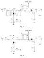
- a circuit according to an embodiment of the invention which increases both ratios K 1 and K 2 is shown in fig. 4.
- a step-up transformer T 2 with a turns ratio of 1:N, has been introduced between the RX port 3 and the shunt diode D 2 .
- This transformer has the effect of increasing the impedance to ground via the RX port 3, as measured at Y, by a factor of N 2 , thereby increasing the ratio K 1 by a factor of N 2 .
- the circuit of fig. 4 also includes a step-down transformer T 1 , with a turns ratio N:1, located between diode D 2 and phase shifting network P 1 .
- the introduction of transformer T 1 has the effect of reducing the impedance of the switched on diode D 2 , as measured at point W in Fig. 4, by a factor of N 2 , and similarly increases the impedance of the switched on diode D 2 , as measured at X (on the far side of phase shifting network P 1 ), by a factor N 2 - see equation 1.
- the introduction of transformer T 1 between diode D 2 and phase shifting network P 1 , has the effect of increasing the ratio K 2 by a factor of N 2 .
- transformer T 2 in fig. 4 should have a turns ratio of 1: ⁇ 2 and transformer T 1 should have a turns ratio of ⁇ 2:1.
- step-up transformer T 2 and a step-down transformer T 1 on either side of diode D 2 , will also result in a reduction of the parasitic resistance R p of the switched-off diode, as measured at node X, in the RX mode of the switch. This has the detrimental effect of increasing the loss of the switch when in RX mode.
- DC blocking capacitors C B are required at the two ground points of transformers T1 and T2 in the circuit of fig. 4 in order to ensure that the diodes D 1 and D 2 can be switched on and off by applying a suitable DC voltage to control voltage terminal VC 1 - see table 2.
- the circuit of fig. 4 can also be configured so that the turns ratio N, of the two transformers, is some value other than ⁇ 2. Increasing N to a value greater than ⁇ 2 will further increase the TX to RX isolation in TX mode. The drawback of increasing N to values higher than ⁇ 2 is that the parallel resistance R p of the switched-off diode is also reduced, and this has the effect of further increasing the loss of the switch in RX mode.
- transformers which operate at the mobile cellular frequency ranges (1 GHz to 2 GHz) are relatively large, and introduce a relatively high insertion loss in the signal path.
- the benefit of the high isolation achievable by the circuit of fig. 4 would have to be weighed up against the increase in size of the switch and the increase in loss along the RX path of the switch.
- impedance transformation can be effected using an LC network. Since the bandwidth for TX and RX of most cellular communications systems is relatively narrow compared with the operating frequency (5% - 10% - see Table 1), an alternative circuit can be devised which uses a pair of impedance transforming LC networks in place of the transformers T 1 and T 2 in the SP2T PIN diode switch of fig. 4. A high isolation SP2T PIN diode switch employing a pair of LC networks for impedance transformation is shown in fig. 5.
- the LC network LC 2 is designed to increase the impedance of the load at the RX port, as measured at node Y, when the switch is in RX mode, and the LC network LC 1 is designed to reduce the impedance back down to its original value.
- the impedance to ground at point W due to the branch of the circuit containing the terminated RX port and LC networks LC 2 and LC 1 , is the same as the impedance measured directly at the RX port 3.
- the impedance transformation properties of an LC network are a function of the load; therefore, in the TX mode of fig. 5 the impedance between node Y and ground, which is dominated by the very small parasitic resistance R s of the switched on diode D2, is not reduced in the same way that it is when the switch is in RX mode (see above). Consequently, for optimum TX operation, the component values of phase shifting network P 1 of fig. 5 must be reduced so that the combined effects of LC 1 and P 1 is to rotate the reflection co-efficient at node Y through an angle of 180° when measured at node X.
- the impedance transformation network LC 2 should have the effect of doubling the impedance of the RX port 3, when measured at node Y, when the switch is in RX mode, and the impedance transformation network LC 1 should have the effect of reducing the impedance of the RX port back down to its original value, when measured at W, and when the switch is in RX mode.
- the circuit of fig. 5 has the benefit of small size, and the further benefit that the capacitors and inductors of the LC networks can be incorporated into a multi-layer substrate, thereby minimising the additional space required for a high isolation PIN diode switch, compared with the conventional PIN switch of fig. 3.
- Fig. 6 shows a circuit which employs a single capacitor C T in place of the two shunt capacitors connected at node Y in fig. 5. This modification has the beneficial effect of further reducing the number of components required to effect high isolation.
- the components L T denote the inductors from each of the impedance transformation networks LC 1 and LC 2 of fig. 5.
- the circuit of fig. 4 disclosed an embodiment of the present invention, the object of which was to increase both ratios K 1 and K 2 , as described above.
- the transformer T 2 of fig. 4 can be replaced by the LC network LC 2 in order to raise the impedance of the RX port when measured at node Y
- the transformer T 1 in the circuit of fig. 4 can be replaced by the LC network LC 1 , which has the effect of reducing the impedance of the RX port back down to 50 ⁇ when measured at point W.
- phase shifting network P 1 has the effect of rotating the complex the reflection co-efficient at point W of fig. 4 through an angle of 180 °, so that it will have a value close to +1 when measured at node X.
- the combination of impedance transformation network LC 1 and phase shifting network P 1 has the effect of rotating the reflection co-efficient at node Y through 180° when measured at X.
- impedance transformation network LC 1 and phase shifting network P 1 of fig. 5 with a simpler circuit as shown in fig. 7, which depicts a fourth embodiment of the present invention.
- the phase shifting network P 1 has been replaced with another circuit P Z , which comprises components C 1 , L 1 and C 2 .
- phase shifting network P Z fulfils the dual role of transforming the impedance at node Y, in RX mode of the switch, back down to 50 Ohms, and rotating the complex reflection co-efficient at node Y, in TX mode of the switch, through an angle of 180° when measured at node X.
- Another approach to achieving higher isolation is to connect a pair of diodes D 2 ' and D 2 '' in parallel in place of the single diode D 2 in fig. 3.
- Such a circuit is shown in fig. 9.
- Connecting diodes D 2 ' and D 2 '' in parallel at node Y halves the parasitic impedance to ground due to the switched on diodes. Consequently, the TX to RX isolation of the SP2T PIN diode switch of fig. 9, when in TX mode, will be improved by approximately 6dB compared with a SP2T PIN switch which uses only a single diode at node Y, such as that shown in fig. 3 - see equation 3.
- TX to RX isolation in TX mode of the switch of fig. 9, can be further be increased by the connection of several diodes in parallel at node Y.
- connecting multiple diodes at node Y has the drawback of reducing the parasitic resistance at node Y when the diodes are switched off; this has the detrimental effect of increasing the loss of the switch when in RX mode.
- An ASM offering ultra-high isolation from the TX port to the RX port, in TX mode can be achieved by the circuit configuration shown in fig. 10, which uses three diodes D 1 , D 2 and D 3 .
- TX mode all three diodes switched on
- this impedance is transformed to a very high value at node Y by the phase shifting network P 2 .
- the low impedance of the switched on diode D 2 , and the resonator comprising L 1 and C 1 gives rise to a second short circuit at node Y.
- a second phase shifting network P 1 transforms the short circuit at node Y to an open circuit at node X (by rotating the complex reflection coefficient through an angle of 180 °), so that the RX branch of the circuit does not load the switch at node X.
- the circuit of fig. 10 is capable of providing approximately two times higher isolation from the TX port 2 to the RX port 3, in TX mode of the switch, when compared with the circuit of fig. 3. For example, using commercially available PIN diodes, an isolation of 56dB approximately is available using the circuit of fig. 10, compared with a TX to RX isolation of 28dB approximately for the SP2T PIN switch of fig. 3.
Landscapes
- Transceivers (AREA)
- Waveguide Switches, Polarizers, And Phase Shifters (AREA)
- Variable-Direction Aerials And Aerial Arrays (AREA)
- Burglar Alarm Systems (AREA)
- Support Of Aerials (AREA)
Priority Applications (5)
| Application Number | Priority Date | Filing Date | Title |
|---|---|---|---|
| DE60315646T DE60315646T2 (de) | 2003-08-15 | 2003-08-15 | Antennenumschaltungsvorrichtung |
| AT03394075T ATE370553T1 (de) | 2003-08-15 | 2003-08-15 | Antennenumschaltungsvorrichtung |
| EP03394075A EP1515450B1 (fr) | 2003-08-15 | 2003-08-15 | Circuit de commutation d'antenne |
| JP2004232953A JP2005065277A (ja) | 2003-08-15 | 2004-08-10 | スイッチング回路 |
| US10/916,140 US7075386B2 (en) | 2003-08-15 | 2004-08-11 | Antenna switching circuit |
Applications Claiming Priority (1)
| Application Number | Priority Date | Filing Date | Title |
|---|---|---|---|
| EP03394075A EP1515450B1 (fr) | 2003-08-15 | 2003-08-15 | Circuit de commutation d'antenne |
Publications (2)
| Publication Number | Publication Date |
|---|---|
| EP1515450A1 true EP1515450A1 (fr) | 2005-03-16 |
| EP1515450B1 EP1515450B1 (fr) | 2007-08-15 |
Family
ID=34130391
Family Applications (1)
| Application Number | Title | Priority Date | Filing Date |
|---|---|---|---|
| EP03394075A Expired - Lifetime EP1515450B1 (fr) | 2003-08-15 | 2003-08-15 | Circuit de commutation d'antenne |
Country Status (5)
| Country | Link |
|---|---|
| US (1) | US7075386B2 (fr) |
| EP (1) | EP1515450B1 (fr) |
| JP (1) | JP2005065277A (fr) |
| AT (1) | ATE370553T1 (fr) |
| DE (1) | DE60315646T2 (fr) |
Cited By (1)
| Publication number | Priority date | Publication date | Assignee | Title |
|---|---|---|---|---|
| DE102004033268A1 (de) * | 2004-07-09 | 2006-02-02 | Atmel Germany Gmbh | Hochfrequenzschaltung |
Families Citing this family (28)
| Publication number | Priority date | Publication date | Assignee | Title |
|---|---|---|---|---|
| US7469131B2 (en) * | 2004-09-14 | 2008-12-23 | Nokia Corporation | Terminal and associated transducer assembly and method for selectively transducing in at least two frequency bands |
| EP1876722B1 (fr) * | 2005-04-28 | 2016-08-24 | Murata Manufacturing Co., Ltd. | Module de commutation a haute frequence et procede d'ajustement de la caracteristique en frequence du circuit a haute frequence |
| US9755681B2 (en) | 2007-09-26 | 2017-09-05 | Intel Mobile Communications GmbH | Radio-frequency front-end and receiver |
| US8390394B2 (en) | 2007-12-19 | 2013-03-05 | Soshin Electric Co., Ltd. | High frequency switch |
| JP5002509B2 (ja) * | 2008-03-28 | 2012-08-15 | 双信電機株式会社 | 高周波スイッチ |
| JP2009152749A (ja) * | 2007-12-19 | 2009-07-09 | Soshin Electric Co Ltd | 信号切替スイッチ |
| JP5158427B2 (ja) * | 2008-05-22 | 2013-03-06 | 横浜ゴム株式会社 | 静電誘導型変換素子の電力取り出し回路 |
| JP5049886B2 (ja) * | 2008-06-06 | 2012-10-17 | 双信電機株式会社 | 高周波スイッチ |
| JP5261119B2 (ja) | 2008-09-30 | 2013-08-14 | 双信電機株式会社 | 高周波スイッチ |
| JP2010114719A (ja) * | 2008-11-07 | 2010-05-20 | Nec Electronics Corp | スイッチング回路 |
| US8374633B2 (en) | 2009-10-05 | 2013-02-12 | Motorola Mobility Llc | Muting indication to enable improved time difference of arrival measurements |
| US8638698B2 (en) * | 2011-07-26 | 2014-01-28 | Motorola Mobility Llc | Front end employing pin diode switch with high linearity and low loss for simultaneous transmission |
| EP2621098B1 (fr) | 2012-01-30 | 2015-07-01 | Telefonaktiebolaget L M Ericsson (Publ) | Émetteur-récepteur et dispositif de communication |
| ES2533314T3 (es) | 2012-06-07 | 2015-04-09 | Telefonaktiebolaget L M Ericsson (Publ) | Transceptor sin duplexor y aparato de comunicación |
| EP2733855B1 (fr) | 2012-11-15 | 2016-07-27 | Telefonaktiebolaget LM Ericsson (publ) | Module frontal émetteur-récepteur |
| US9306613B2 (en) | 2013-01-10 | 2016-04-05 | Google Technology Holdings LLC | Variable antenna match linearity |
| EP2974048B1 (fr) | 2013-03-14 | 2021-06-23 | Telefonaktiebolaget LM Ericsson (publ) | Réduction de fuite d'émetteur-récepteur dans un système duplex intégral sans utiliser de duplexeur |
| US20140273887A1 (en) * | 2013-03-15 | 2014-09-18 | Motorola Mobility Llc | Tunable ila and dila matching for simultaneous high and low band operation |
| US10027465B2 (en) | 2013-04-26 | 2018-07-17 | Telefonaktiebolaget Lm Ericsson | Transceiver arrangement, communication device, method and computer program |
| MY185907A (en) | 2013-04-30 | 2021-06-14 | Ericsson Telefon Ab L M | Transceiver arrangement, communication device, method and computer program |
| EP3097645B1 (fr) | 2014-01-21 | 2017-08-23 | Telefonaktiebolaget LM Ericsson (publ) | Montage émetteur-récepteur et dispositif de communication |
| JP2014112907A (ja) * | 2014-01-22 | 2014-06-19 | Nec Corp | アンテナスイッチ回路及び通信端末 |
| EP3213419B1 (fr) | 2014-10-29 | 2019-01-02 | Telefonaktiebolaget LM Ericsson (publ) | Configuration d'émetteur-récepteur et dispositif de communication |
| EP3079204B1 (fr) * | 2015-04-09 | 2021-04-07 | The Boeing Company | Antenne à surface d'impédance artificielle dirigeable électroniquement de manière bidimensionnelle |
| US10270427B2 (en) | 2015-12-07 | 2019-04-23 | Qorvo International Pte. Ltd. | On-chip balun circuit and multi-port antenna switch circuit |
| CN108683434B (zh) * | 2018-08-29 | 2018-12-07 | 上海亮牛半导体科技有限公司 | 适用于恒包络非线性调制的片上集成收发匹配网络及方法 |
| WO2020198349A1 (fr) * | 2019-03-25 | 2020-10-01 | The Texas A&M University System | Modules de duplexeur intégral entièrement intégrés à ondes millimétriques avec et sans amplificateur à faible bruit interne et amplificateur de puissance pour des applications 5g |
| US11323147B1 (en) * | 2021-06-07 | 2022-05-03 | Futurecom Systems Group, ULC | Reducing insertion loss in a switch for a communication device |
Citations (6)
| Publication number | Priority date | Publication date | Assignee | Title |
|---|---|---|---|---|
| FR2703536A1 (fr) * | 1993-03-31 | 1994-10-07 | Motorola Inc | Circuit de commutation et procédé associé. |
| EP0641090A2 (fr) * | 1993-08-31 | 1995-03-01 | Matsushita Electric Industrial Co., Ltd. | Commutateur d'antenne |
| US5442812A (en) * | 1992-07-08 | 1995-08-15 | Matsushita Electric Industrial Co., Ltd. | Antenna switching apparatus for selectively connecting antenna to transmitter or receiver |
| EP1087538A2 (fr) * | 1999-09-24 | 2001-03-28 | Matsushita Electric Industrial Co., Ltd. | Commutateur d'émission-réception |
| US6249670B1 (en) * | 1997-01-13 | 2001-06-19 | Telefonaktiebolaget Lm Ericsson (Publ) | Signal combining device and method for radio communication |
| EP1126624A2 (fr) * | 2000-01-21 | 2001-08-22 | Murata Manufacturing Co., Ltd. | Commutateur de radiofréquence |
Family Cites Families (5)
| Publication number | Priority date | Publication date | Assignee | Title |
|---|---|---|---|---|
| FI102121B (fi) * | 1995-04-07 | 1998-10-15 | Filtronic Lk Oy | Radiotietoliikenteen lähetin/vastaanotin |
| WO1997004533A1 (fr) * | 1995-07-19 | 1997-02-06 | Tdk Corporation | Commutateur d'antenne |
| JP3220679B2 (ja) * | 1997-06-03 | 2001-10-22 | 松下電器産業株式会社 | 2周波スイッチ、2周波アンテナ共用器およびそれを用いた2周波帯域用移動体通信機器 |
| EP1223634A3 (fr) * | 2000-12-26 | 2003-08-13 | Matsushita Electric Industrial Co., Ltd. | Commutateur haute fréquence, commutateur laminé haute fréquence, unité de radio haute fréquence et méthode de commutation haute fréquence |
| JP2004153523A (ja) * | 2002-10-30 | 2004-05-27 | Matsushita Electric Ind Co Ltd | 高周波スイッチモジュール |
-
2003
- 2003-08-15 EP EP03394075A patent/EP1515450B1/fr not_active Expired - Lifetime
- 2003-08-15 DE DE60315646T patent/DE60315646T2/de not_active Expired - Fee Related
- 2003-08-15 AT AT03394075T patent/ATE370553T1/de not_active IP Right Cessation
-
2004
- 2004-08-10 JP JP2004232953A patent/JP2005065277A/ja not_active Withdrawn
- 2004-08-11 US US10/916,140 patent/US7075386B2/en not_active Expired - Fee Related
Patent Citations (6)
| Publication number | Priority date | Publication date | Assignee | Title |
|---|---|---|---|---|
| US5442812A (en) * | 1992-07-08 | 1995-08-15 | Matsushita Electric Industrial Co., Ltd. | Antenna switching apparatus for selectively connecting antenna to transmitter or receiver |
| FR2703536A1 (fr) * | 1993-03-31 | 1994-10-07 | Motorola Inc | Circuit de commutation et procédé associé. |
| EP0641090A2 (fr) * | 1993-08-31 | 1995-03-01 | Matsushita Electric Industrial Co., Ltd. | Commutateur d'antenne |
| US6249670B1 (en) * | 1997-01-13 | 2001-06-19 | Telefonaktiebolaget Lm Ericsson (Publ) | Signal combining device and method for radio communication |
| EP1087538A2 (fr) * | 1999-09-24 | 2001-03-28 | Matsushita Electric Industrial Co., Ltd. | Commutateur d'émission-réception |
| EP1126624A2 (fr) * | 2000-01-21 | 2001-08-22 | Murata Manufacturing Co., Ltd. | Commutateur de radiofréquence |
Cited By (1)
| Publication number | Priority date | Publication date | Assignee | Title |
|---|---|---|---|---|
| DE102004033268A1 (de) * | 2004-07-09 | 2006-02-02 | Atmel Germany Gmbh | Hochfrequenzschaltung |
Also Published As
| Publication number | Publication date |
|---|---|
| ATE370553T1 (de) | 2007-09-15 |
| US7075386B2 (en) | 2006-07-11 |
| EP1515450B1 (fr) | 2007-08-15 |
| US20050035824A1 (en) | 2005-02-17 |
| DE60315646D1 (de) | 2007-09-27 |
| JP2005065277A (ja) | 2005-03-10 |
| DE60315646T2 (de) | 2008-07-17 |
Similar Documents
| Publication | Publication Date | Title |
|---|---|---|
| EP1515450B1 (fr) | Circuit de commutation d'antenne | |
| US6847829B2 (en) | Multiband high-frequency switch | |
| JP4243532B2 (ja) | スイッチング回路 | |
| US6400963B1 (en) | Harmonic suppression in dual band mobile phones | |
| US6795714B1 (en) | Multiband antenna switcher | |
| US20020137471A1 (en) | High-frequency composite switch component | |
| US20100091690A1 (en) | Distribution diplexer | |
| WO2005101670A2 (fr) | Appareil, procedes et articles manufactures destines a l'adaptation d'impedance de sortie utilisant un traitement de signaux multibandes | |
| JP3810011B2 (ja) | 高周波スイッチモジュールおよび高周波スイッチモジュール用多層基板 | |
| US20070080756A1 (en) | BAW duplexer without phase shifter | |
| US10270485B2 (en) | Switch module and radio-frequency module | |
| EP1583254A1 (fr) | Diplexeur et circuit d'adapation | |
| KR20110130389A (ko) | Rf 전단 모듈 및 안테나 시스템 | |
| US10284165B2 (en) | Variable phase shifter, variable phase shift circuit, RF front-end circuit, and communication apparatus | |
| KR20010042499A (ko) | 안테나 스위치 | |
| GB2333669A (en) | High-frequency circuit device | |
| GB2515459A (en) | Duplexers | |
| JP2010521830A (ja) | Rfスイッチ及びrfスイッチを備える装置 | |
| JP2000349580A (ja) | 周波数特性可変フィルタ、アンテナ共用器および通信装置 | |
| KR20200100129A (ko) | 멀티플렉서, 고주파 프런트엔드 회로 및 통신 장치 | |
| JP2004146916A (ja) | 高周波スイッチ回路および高周波スイッチモジュール | |
| JP2003133992A (ja) | 高周波回路 | |
| JP2002208802A (ja) | 帯域可変型フィルタ回路及びそれを用いた高周波フロントエンド回路 | |
| JP2002198855A (ja) | 送受信制御回路 | |
| KR20070017356A (ko) | 다중 대역 신호 처리를 이용한 출력 임피던스 정합 장치,방법 및 구성품 |
Legal Events
| Date | Code | Title | Description |
|---|---|---|---|
| PUAI | Public reference made under article 153(3) epc to a published international application that has entered the european phase |
Free format text: ORIGINAL CODE: 0009012 |
|
| AK | Designated contracting states |
Kind code of ref document: A1 Designated state(s): AT BE BG CH CY CZ DE DK EE ES FI FR GB GR HU IE IT LI LU MC NL PT RO SE SI SK TR |
|
| AX | Request for extension of the european patent |
Extension state: AL LT LV MK |
|
| 17P | Request for examination filed |
Effective date: 20050916 |
|
| AKX | Designation fees paid |
Designated state(s): AT BE BG CH CY CZ DE DK EE ES FI FR GB GR HU IE IT LI LU MC NL PT RO SE SI SK TR |
|
| GRAP | Despatch of communication of intention to grant a patent |
Free format text: ORIGINAL CODE: EPIDOSNIGR1 |
|
| GRAS | Grant fee paid |
Free format text: ORIGINAL CODE: EPIDOSNIGR3 |
|
| GRAA | (expected) grant |
Free format text: ORIGINAL CODE: 0009210 |
|
| AK | Designated contracting states |
Kind code of ref document: B1 Designated state(s): AT BE BG CH CY CZ DE DK EE ES FI FR GB GR HU IE IT LI LU MC NL PT RO SE SI SK TR |
|
| REG | Reference to a national code |
Ref country code: GB Ref legal event code: FG4D |
|
| REG | Reference to a national code |
Ref country code: CH Ref legal event code: EP |
|
| REG | Reference to a national code |
Ref country code: IE Ref legal event code: FG4D |
|
| REF | Corresponds to: |
Ref document number: 60315646 Country of ref document: DE Date of ref document: 20070927 Kind code of ref document: P |
|
| PG25 | Lapsed in a contracting state [announced via postgrant information from national office to epo] |
Ref country code: BG Free format text: LAPSE BECAUSE OF FAILURE TO SUBMIT A TRANSLATION OF THE DESCRIPTION OR TO PAY THE FEE WITHIN THE PRESCRIBED TIME-LIMIT Effective date: 20071115 Ref country code: FI Free format text: LAPSE BECAUSE OF FAILURE TO SUBMIT A TRANSLATION OF THE DESCRIPTION OR TO PAY THE FEE WITHIN THE PRESCRIBED TIME-LIMIT Effective date: 20070815 Ref country code: NL Free format text: LAPSE BECAUSE OF FAILURE TO SUBMIT A TRANSLATION OF THE DESCRIPTION OR TO PAY THE FEE WITHIN THE PRESCRIBED TIME-LIMIT Effective date: 20070815 Ref country code: ES Free format text: LAPSE BECAUSE OF FAILURE TO SUBMIT A TRANSLATION OF THE DESCRIPTION OR TO PAY THE FEE WITHIN THE PRESCRIBED TIME-LIMIT Effective date: 20071126 |
|
| NLV1 | Nl: lapsed or annulled due to failure to fulfill the requirements of art. 29p and 29m of the patents act | ||
| ET | Fr: translation filed | ||
| PG25 | Lapsed in a contracting state [announced via postgrant information from national office to epo] |
Ref country code: LI Free format text: LAPSE BECAUSE OF FAILURE TO SUBMIT A TRANSLATION OF THE DESCRIPTION OR TO PAY THE FEE WITHIN THE PRESCRIBED TIME-LIMIT Effective date: 20070815 Ref country code: AT Free format text: LAPSE BECAUSE OF FAILURE TO SUBMIT A TRANSLATION OF THE DESCRIPTION OR TO PAY THE FEE WITHIN THE PRESCRIBED TIME-LIMIT Effective date: 20070815 Ref country code: CH Free format text: LAPSE BECAUSE OF FAILURE TO SUBMIT A TRANSLATION OF THE DESCRIPTION OR TO PAY THE FEE WITHIN THE PRESCRIBED TIME-LIMIT Effective date: 20070815 |
|
| REG | Reference to a national code |
Ref country code: CH Ref legal event code: PL |
|
| PG25 | Lapsed in a contracting state [announced via postgrant information from national office to epo] |
Ref country code: BE Free format text: LAPSE BECAUSE OF FAILURE TO SUBMIT A TRANSLATION OF THE DESCRIPTION OR TO PAY THE FEE WITHIN THE PRESCRIBED TIME-LIMIT Effective date: 20070815 |
|
| PG25 | Lapsed in a contracting state [announced via postgrant information from national office to epo] |
Ref country code: MC Free format text: LAPSE BECAUSE OF NON-PAYMENT OF DUE FEES Effective date: 20070831 Ref country code: GR Free format text: LAPSE BECAUSE OF FAILURE TO SUBMIT A TRANSLATION OF THE DESCRIPTION OR TO PAY THE FEE WITHIN THE PRESCRIBED TIME-LIMIT Effective date: 20071116 Ref country code: DK Free format text: LAPSE BECAUSE OF FAILURE TO SUBMIT A TRANSLATION OF THE DESCRIPTION OR TO PAY THE FEE WITHIN THE PRESCRIBED TIME-LIMIT Effective date: 20070815 |
|
| PG25 | Lapsed in a contracting state [announced via postgrant information from national office to epo] |
Ref country code: CZ Free format text: LAPSE BECAUSE OF FAILURE TO SUBMIT A TRANSLATION OF THE DESCRIPTION OR TO PAY THE FEE WITHIN THE PRESCRIBED TIME-LIMIT Effective date: 20070815 Ref country code: PT Free format text: LAPSE BECAUSE OF FAILURE TO SUBMIT A TRANSLATION OF THE DESCRIPTION OR TO PAY THE FEE WITHIN THE PRESCRIBED TIME-LIMIT Effective date: 20080115 Ref country code: SK Free format text: LAPSE BECAUSE OF FAILURE TO SUBMIT A TRANSLATION OF THE DESCRIPTION OR TO PAY THE FEE WITHIN THE PRESCRIBED TIME-LIMIT Effective date: 20070815 |
|
| PLBE | No opposition filed within time limit |
Free format text: ORIGINAL CODE: 0009261 |
|
| STAA | Information on the status of an ep patent application or granted ep patent |
Free format text: STATUS: NO OPPOSITION FILED WITHIN TIME LIMIT |
|
| PG25 | Lapsed in a contracting state [announced via postgrant information from national office to epo] |
Ref country code: SE Free format text: LAPSE BECAUSE OF FAILURE TO SUBMIT A TRANSLATION OF THE DESCRIPTION OR TO PAY THE FEE WITHIN THE PRESCRIBED TIME-LIMIT Effective date: 20071115 Ref country code: RO Free format text: LAPSE BECAUSE OF FAILURE TO SUBMIT A TRANSLATION OF THE DESCRIPTION OR TO PAY THE FEE WITHIN THE PRESCRIBED TIME-LIMIT Effective date: 20070815 |
|
| 26N | No opposition filed |
Effective date: 20080516 |
|
| PG25 | Lapsed in a contracting state [announced via postgrant information from national office to epo] |
Ref country code: IE Free format text: LAPSE BECAUSE OF NON-PAYMENT OF DUE FEES Effective date: 20070815 |
|
| PGFP | Annual fee paid to national office [announced via postgrant information from national office to epo] |
Ref country code: DE Payment date: 20080828 Year of fee payment: 6 |
|
| PGFP | Annual fee paid to national office [announced via postgrant information from national office to epo] |
Ref country code: FR Payment date: 20080317 Year of fee payment: 6 |
|
| PGFP | Annual fee paid to national office [announced via postgrant information from national office to epo] |
Ref country code: GB Payment date: 20080827 Year of fee payment: 6 |
|
| PG25 | Lapsed in a contracting state [announced via postgrant information from national office to epo] |
Ref country code: EE Free format text: LAPSE BECAUSE OF FAILURE TO SUBMIT A TRANSLATION OF THE DESCRIPTION OR TO PAY THE FEE WITHIN THE PRESCRIBED TIME-LIMIT Effective date: 20070815 |
|
| PG25 | Lapsed in a contracting state [announced via postgrant information from national office to epo] |
Ref country code: SI Free format text: LAPSE BECAUSE OF FAILURE TO SUBMIT A TRANSLATION OF THE DESCRIPTION OR TO PAY THE FEE WITHIN THE PRESCRIBED TIME-LIMIT Effective date: 20070815 |
|
| PG25 | Lapsed in a contracting state [announced via postgrant information from national office to epo] |
Ref country code: CY Free format text: LAPSE BECAUSE OF FAILURE TO SUBMIT A TRANSLATION OF THE DESCRIPTION OR TO PAY THE FEE WITHIN THE PRESCRIBED TIME-LIMIT Effective date: 20070815 |
|
| PG25 | Lapsed in a contracting state [announced via postgrant information from national office to epo] |
Ref country code: LU Free format text: LAPSE BECAUSE OF NON-PAYMENT OF DUE FEES Effective date: 20070815 |
|
| PG25 | Lapsed in a contracting state [announced via postgrant information from national office to epo] |
Ref country code: TR Free format text: LAPSE BECAUSE OF FAILURE TO SUBMIT A TRANSLATION OF THE DESCRIPTION OR TO PAY THE FEE WITHIN THE PRESCRIBED TIME-LIMIT Effective date: 20070815 Ref country code: HU Free format text: LAPSE BECAUSE OF FAILURE TO SUBMIT A TRANSLATION OF THE DESCRIPTION OR TO PAY THE FEE WITHIN THE PRESCRIBED TIME-LIMIT Effective date: 20080216 |
|
| GBPC | Gb: european patent ceased through non-payment of renewal fee |
Effective date: 20090815 |
|
| REG | Reference to a national code |
Ref country code: FR Ref legal event code: ST Effective date: 20100430 |
|
| PG25 | Lapsed in a contracting state [announced via postgrant information from national office to epo] |
Ref country code: FR Free format text: LAPSE BECAUSE OF NON-PAYMENT OF DUE FEES Effective date: 20090831 Ref country code: DE Free format text: LAPSE BECAUSE OF NON-PAYMENT OF DUE FEES Effective date: 20100302 |
|
| PG25 | Lapsed in a contracting state [announced via postgrant information from national office to epo] |
Ref country code: GB Free format text: LAPSE BECAUSE OF NON-PAYMENT OF DUE FEES Effective date: 20090815 |
|
| PG25 | Lapsed in a contracting state [announced via postgrant information from national office to epo] |
Ref country code: IT Free format text: LAPSE BECAUSE OF NON-PAYMENT OF DUE FEES Effective date: 20070831 |