EP1513192A1 - Halbleiterwafer - Google Patents
Halbleiterwafer Download PDFInfo
- Publication number
- EP1513192A1 EP1513192A1 EP03733337A EP03733337A EP1513192A1 EP 1513192 A1 EP1513192 A1 EP 1513192A1 EP 03733337 A EP03733337 A EP 03733337A EP 03733337 A EP03733337 A EP 03733337A EP 1513192 A1 EP1513192 A1 EP 1513192A1
- Authority
- EP
- European Patent Office
- Prior art keywords
- wafer
- semiconductor wafer
- shape
- outer peripheral
- peripheral portion
- Prior art date
- Legal status (The legal status is an assumption and is not a legal conclusion. Google has not performed a legal analysis and makes no representation as to the accuracy of the status listed.)
- Withdrawn
Links
Images


Classifications
-
- B—PERFORMING OPERATIONS; TRANSPORTING
- B24—GRINDING; POLISHING
- B24B—MACHINES, DEVICES, OR PROCESSES FOR GRINDING OR POLISHING; DRESSING OR CONDITIONING OF ABRADING SURFACES; FEEDING OF GRINDING, POLISHING, OR LAPPING AGENTS
- B24B37/00—Lapping machines or devices; Accessories
- B24B37/04—Lapping machines or devices; Accessories designed for working plane surfaces
- B24B37/042—Lapping machines or devices; Accessories designed for working plane surfaces operating processes therefor
-
- H—ELECTRICITY
- H10—SEMICONDUCTOR DEVICES; ELECTRIC SOLID-STATE DEVICES NOT OTHERWISE PROVIDED FOR
- H10P—GENERIC PROCESSES OR APPARATUS FOR THE MANUFACTURE OR TREATMENT OF DEVICES COVERED BY CLASS H10
- H10P95/00—Generic processes or apparatus for manufacture or treatments not covered by the other groups of this subclass
-
- B—PERFORMING OPERATIONS; TRANSPORTING
- B24—GRINDING; POLISHING
- B24B—MACHINES, DEVICES, OR PROCESSES FOR GRINDING OR POLISHING; DRESSING OR CONDITIONING OF ABRADING SURFACES; FEEDING OF GRINDING, POLISHING, OR LAPPING AGENTS
- B24B9/00—Machines or devices designed for grinding edges or bevels on work or for removing burrs; Accessories therefor
-
- H—ELECTRICITY
- H10—SEMICONDUCTOR DEVICES; ELECTRIC SOLID-STATE DEVICES NOT OTHERWISE PROVIDED FOR
- H10P—GENERIC PROCESSES OR APPARATUS FOR THE MANUFACTURE OR TREATMENT OF DEVICES COVERED BY CLASS H10
- H10P74/00—Testing or measuring during manufacture or treatment of wafers, substrates or devices
Definitions
- the present invention relates to a semiconductor wafer typified by silicon wafers, and more particularly to a semiconductor wafer shape.
- CMOS single crystal ingots in cylindrical form are grown by the Czochralski (CZ) method, the Floating Zone (FZ) method or other method, and the grown semiconductor single crystal ingots are sliced into wafers in thin plate form, followed by subjecting the obtained wafers to steps such as a chamfering step for chamfering outer peripheral portions of wafers to prevent cracks and chips in wafers, a lapping step for adjusting the wafer thickness and flatness, an etching step for etching wafers to remove mechanical damage from wafers, a polishing step for further improving surface roughness and flatness of etched wafers to make the wafer surfaces into mirror surfaces, and a cleaning step for cleaning wafers to remove polishing agent and foreign substances from wafers.
- CZ Czochralski
- FZ Floating Zone
- steps in which thin films such as oxide films, metal films or polysilicon films are formed in layers on a semiconductor wafer to form a resist pattern are normally performed about 20 to 30 times, for example.
- DRAM dynamic random access memory
- a resist pattern with line width of 0.25 ⁇ m to 0.20 ⁇ m is formed on currently mass-produced 64M-bit DRAM.
- the CMP Chemical Mechanical Polishing
- polishing is performed useing multilayered elastic polishing pads, and therefore uniform stock removal can be obtained.
- the aforementioned CMP technique - the technique that provides uniform stock removal - is used in the polishing step, thus performing a smooth and damage-free mirror-polishing.
- the CMP technique is designed on the principle of achieving polishing by chemical and mechanical effects, and, for example, polishing is conducted by rubbing a wafer and a polishing pad relatively to each other under a given load while supplying a polishing agent in which colloidal silica is dispersed in alkali solution.
- a soft silica hydrate film is formed on the wafer surface by the alkali solution, and polishing proceeds as this hydrate film is removed.
- polishing is conducted more often by a CMP polishing apparatus with a polishing head using a retainer ring that pushes in the polishing pad at the wafer periphery for preventing excessive polishing of the outer peripheral portion to prevent peripheral sag.
- the present invention was accomplished in light of the foregoing, and it is an object of the present invention to provide a semiconductor wafer capable of forming device patterns on the wafer with high yield despite shape variation in a wafer chuck of an exposure apparatus in the photolithography step and polishing the wafer with uniform stock removal in CMP in a device production process.
- a semiconductor wafer wherein the semiconductor wafer has a shape in which the outer peripheral portion of the semiconductor wafer bends in such a manner as to swell (rises) on the wafer front surface and bends in such a manner as to droop (sags) on the wafer back surface.
- the semiconductor wafer constitutes not only a preferred wafer for a variety of exposure apparatuses used commonly for the photolithography step but also a wafer capable of performing CMP with uniform stock removal, if the outer peripheral portion thereof bends in such a manner as to swell (rises) on the wafer front surface and bends in such a manner as to droop (sags) on the wafer back surface.
- the wafer front surface refers to one of the wafer main surfaces - the surface on which devices, etc. are formed - and the wafer back surface to the other wafer main surface.
- the bend of the outer peripheral portion of the semiconductor wafer is preferably such that, when performing measurement of shape data on the front and back surfaces of the semiconductor wafer, creation of respective shape profiles along the radial direction from the measured shape data on the front and back surfaces of the wafer and calculation of differential profiles through differential processing of the created respective shape profiles, the differential profile of the wafer front surface exhibits a bend like swelling (rise) at the outer peripheral portion and the differential profile of the wafer back surface exhibits a bend like drooping (sag) at the outer peripheral portion.
- the differential profile of the wafer front surface exhibits a bend like swelling (rise) at the outer peripheral portion - that is, the differential value of the differential profile (magnitude of slope ⁇ m/mm) changes on the positive side when rise is expressed as positive - and if the differential profile of the wafer back surface exhibits a bend like drooping (sag) at the peripheral portion - that is, the differential value of the differential profile (magnitude of slope ⁇ m/mm) changes on the negative side when sag is expressed as negative, then it is possible to make a semiconductor wafer having different shapes between the front and back surfaces which could not be confirmed accurately by the conventional indicators based on wafer thickness into a quantitatively and accurately prescribed wa
- the front and back surfaces of the semiconductor wafer bend in a region of the outer peripheral portion excluding 1mm to 2mm from the outermost periphery of the semiconductor wafer.
- the shape of the outer peripheral portion in the region where devices are actually formed is important.
- the area (specification) guaranteed for flatness in wafers supplied to the device production process has conventionally often been the area excluding 3mm from the outermost peripheral portion of the wafers (the region toward the center of wafers excluding this portion is occasionally referred to as wafer effective region).
- the shape of the wafer according to the present invention is at least such that the outer peripheral portion in the wafer effective region bends in such a manner as to swell (rises) on the wafer front surface and bends in such a manner as to droop (sags) on the wafer back surface.
- the guaranteed area is the area excluding 3mm from the outermost peripheral portion of the wafer
- bend occurs up to the region of the outer peripheral portion excluding 2mm from the outermost periphery (end portion) of the semiconductor wafer and further up to the region excluding 1mm from the outermost periphery (end portion).
- the semiconductor wafer is formed to have a bend occurring up to such a region, it is possible to considerably reduce generation of defocus failure, discoloration failure due to CMP and the like within the guaranteed area.
- a chamfered portion is formed on the outermost periphery of the semiconductor wafer, it is preferred that a bend occurs in the region of the outer peripheral portion excluding 1mm or less from the outermost periphery of the semiconductor wafer on both front and back surfaces. This ensures that the semiconductor wafer constitutes a preferred wafer for both exposure apparatuses used in the photolithography step and for polishing by CMP.
- the rise start position on the front surface (turning point on the front surface) and the sag start position on the back surface (turning point on the back surface) at the outer peripheral portion of the semiconductor wafer lie in a region within 10mm from the outermost periphery of the wafer.
- the wafer shape at the outer peripheral portion and particularly in the region within 10mm from the wafer outermost periphery is extremely important. Consequently, the semiconductor wafer can constitute a preferred wafer for both exposure apparatus used in the photolithography step and for polishing by CMP, if the rise start position on the front surface (turning point on the front surface) and the sag start position on the back surface (turning point on the back surface) at the outer peripheral portion of the semiconductor wafer lie in a region within 10mm from the outermost periphery of the wafer as in the present invention.
- the rise start position on the front surface (turning point on the front surface) and the sag start position on the back surface (turning point on the back surface) of the semiconductor wafer are preferably located at the same distance from the wafer center along the wafer radial direction.
- the turning points on the front and back surfaces of the semiconductor wafer are located at the same distance from the wafer center along the wafer radial direction, it is possible to ensure a semiconductor wafer having approximately uniform thickness at the device fabrication region in the wafer plane, despite different shapes on the front and back surfaces of the semiconductor wafer. Consequently, since the semiconductor wafer front surface can be kept in a flat state by vacuum absorption of the wafer using a vacuum chuck in the photolithography step, for example, it is possible to accurately form patterns on the wafer front surface.
- the front and back surfaces of the semiconductor wafer are preferably mirror-polished.
- the semiconductor wafer can be have higher flatness if the front and back surfaces thereof are mirror-polished. Therefore, it is possible to fabricate devices with high precision on the semiconductor wafer, further improving yield in device production.
- a semiconductor wafer that is preferred for exposure apparatus commonly used in the photolithography step and that has a shape capable of performing CMP with uniform stock removal.
- Such a semiconductor wafer according to the present invention allows accurate formation of device patterns on the wafer front surface while remaining free of uneven film thickness and discoloration even in performing CMP in the device production process, and therefore yield in semiconductor device production can be improved.
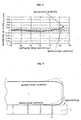
- Fig. 1 illustrates a schematic explanatory view describing the shape of a semiconductor wafer of the present invention.
- Fig. 1 shows the features of the present invention in exaggerated fashion for clarity of presentation, and proportionality relation of the sizes and figures and so on are different from an actual wafer. The present invention is in no way limited thereby.
- a semiconductor wafer 1 of the present invention is characterized in that the wafer has a shape in which the outer peripheral portion of the semiconductor wafer bends in such a manner as to swell (rises) on the wafer front surface and bends in such a manner as to droop (sags) on the wafer back surface.
- the semiconductor wafer of the present invention has different shapes between on the front and back surfaces, with the wafer outer peripheral portion bending on the wafer front surface so as to be more convex than the wafer surface position at the center portion of the front surface (this bend is referred to as "rise”) and bending on the wafer back surface so as to be more concave than the wafer surface position at the center portion of the back surface (this bend is referred to as "sag").
- the semiconductor wafer of the present invention is a wafer in which when subjected to measurement of shape data on both front and back surfaces of the semiconductor wafer, creation of shape profiles along the radial direction from the measured shape data of the front and back surfaces of the wafer, and calculation of differential profiles through differential processing of the respective created shape profiles, the differential profile of the wafer front surface exhibits a bend like swelling (rise) at the outer peripheral portion, and the differential profile of the wafer back surface exhibits a bend like drooping (sag) at the outer peripheral portion.
- the semiconductor wafer having different shapes between the front and back surfaces can be quantitatively expressed if the semiconductor wafer shape is prescribed by the aforementioned method, that is, the differential type shape evaluation system. Therefore, the semiconductor wafer can reliably have a shape such that rise is formed on the front surface and sag is formed on the back surface.
- the method will be described below for prescribing the shape of the semiconductor wafer of the present invention by the differential type shape evaluation system with reference to the accompanying drawings.
- shape data of the front and back surfaces of the semiconductor wafer is measured.
- Shape data measurement of the semiconductor wafer can be conducted, for example, using shape measurement means 8 shown in Fig. 6.
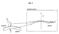
- Shape data of the front and back surfaces of the semiconductor wafer 1 can be obtained by holding part of the outer peripheral portion or the main surface of the semiconductor wafer by a wafer holder 9, scanning the semiconductor wafer with two displacement gauges 10 of front and back arranged so as to sandwich the wafer 1 and thereby measuring the displacement of surface along the wafer thickness direction.
- the shape of the semiconductor wafer can be evaluated with excellent precision by scanning the front and back surfaces of the semiconductor wafer at fine measurement intervals. For instance, it is possible to measure the shape data of the semiconductor wafer with excellent measurement precision by setting the semiconductor wafer scanning intervals to 1mm or less and particularly about 0.05mm.
- the shape data is obtained by placing a semiconductor wafer without absorption on the specimen table for holding a target to be measured, scanning the front or back surface of the semiconductor wafer with a displacement gauge and measuring the displacement of surface along the wafer thickness direction, for example.
- shape profiles along the radial direction are created respectively for the front and back surfaces of the semiconductor wafer from the measured shape data of the front and back surfaces of the semiconductor wafer.
- shape profiles of the wafer outer peripheral portion as shown in Fig. 2 are created.
- the shape profiles of Fig. 2 show data of the shape in the region of 120 to 148mm from the wafer center of the semiconductor wafer having a diameter of 300mm. At this time, the region of 2mm from the outermost periphery of the wafer was excluded from measurement. As is apparent from the figure, mere observation of the shape profile (displacement) does not lead to an accurate judgment as to whether the outer peripheral shape becomes sag or rise and where the shape change begins because of considerable effects of waviness, etc.
- a chamfered portion is formed as shown in Fig. 1.
- the width of the chamfered portion varies depending on the wafer production method but is normally about 500 ⁇ m (0.5mm). Considering factors such as measurement precision, it suffices to exclude the region of 1mm from the outermost periphery of the semiconductor wafer including the chamfered portion. Further, the region toward the center of the wafer excluding the region within 1mm to 2mm from the wafer outer periphery is of prime importance in the semiconductor wafer of the present invention.
- the semiconductor wafer of the present invention constitutes a preferred wafer for exposure apparatus used in the photolithography step and for performing CMP, if the front and back surfaces of the semiconductor wafer of the present invention has a bend in a region excluding the measurement exclusion region within 1mm to 2mm from the outermost periphery of the semiconductor wafer including the chamfered portion.
- shape profile shape data
- shape data of the semiconductor wafer is measured using the shape measurement means 8 shown in Fig. 6, the shape data is obtained by the displacement gauges 10 as shown in Fig. 7. Therefore, the shape data of the wafer back surface is represented with the opposite sign in terms of positive and negative to that used in the shape data of the wafer front surface.
- the created shape profiles (Fig. 2) are differentiated with respect to an arbitrary position at constant intervals. Then, by plotting data at the midpoint thereof, differential profiles can be calculated as shown in Fig. 3. That is, as the basis for an arbitrary point X i (mm) in the created shape profiles, it is possible to calculate differential profiles by calculating the quotient of the difference between a magnitude of displacement of the shape profile Y i+1 ( ⁇ m) at X i+1 (mm) and a magnitude of displacement of the shape profile Y i ( ⁇ m) at X i (mm) divided by a constant interval (X i+1 - X i ) as a differential value (dyi), and then plotting the data at the midpoint of the interval (X i+1 - X i ) .
- the differential value corresponds to a magnitude of slope ( ⁇ m/mm).
- the differential profiles in Fig. 3 are obtained by subjecting to least square approximation for removing the long wavelength component and also performing an operation of moving average of about 1 to 2mm for removing measurement noises during calculation of differential profiles from the shape profiles.
- the interval (X i+1 - X i ) for which differentiation of the shape profile is performed can be selected arbitrarily according to the shape of the semiconductor wafer to be evaluated, if the shape profiles are subjected to differentiation at 1mm-intervals along the wafer radial direction, the shape of the semiconductor wafer can be prescribed with high precision.
- the semiconductor wafer of the present invention is a wafer in which the differential profile thus obtained exhibits a bend like swelling (rise) on the outer peripheral portion of the wafer front surface - that is, the differential value of the differential profile (magnitude of slope ⁇ m/mm) changes on the positive side when rise is expressed as positive - and exhibits a bend like drooping (sag) on the outer peripheral portion of the wafer back surface - that is, the differential value of the differential profile (magnitude of slope ⁇ m/mm) changes on the negative side when sag is expressed as negative.
- the differential profile thus obtained exhibits a bend like swelling (rise) on the outer peripheral portion of the wafer front surface - that is, the differential value of the differential profile (magnitude of slope ⁇ m/mm) changes on the positive side when rise is expressed as positive - and exhibits a bend like drooping (sag) on the outer peripheral portion of the wafer back surface - that is, the differential value of the differential profile (magnitude
- the semiconductor wafer of the present invention has a shape in which the differential profile of the wafer front surface shows positive within the evaluation region at the outer peripheral portion as in the differential profile shown in Fig. 3, for example, if the wafer surface slope in the direction of increasing wafer thickness on the wafer front surface is expressed as positive.
- the semiconductor wafer of the present invention has a shape in which the differential profile of the wafer back surface shows positive within the evaluation region at the outer peripheral portion, for example, if the wafer surface slope in the direction of decreasing wafer thickness on the wafer back surface is expressed as positive.
- the shape of the semiconductor wafer according to the differential type shape evaluation system, it is possible to quantitatively and accurately indicate the shape of the semiconductor wafer as in the present invention, which has been not confirmed accurately by the conventional evaluation of the semiconductor wafer based on wafer thickness, that is, shape in which rise is formed on the front surface and sag is formed on the back surface of the wafer outer peripheral portion. Therefore, it is possible to accurately and clearly define the wafer shape by prescribing the shape of the wafer outer peripheral portion using the evaluation method.
- the semiconductor wafer of the present invention bends in the region of the outer peripheral portion excluding the measurement exclusion region which is within 1mm to 2mm from the outermost periphery of the semiconductor wafer on the front and back surfaces of the wafer as shown in Fig. 1, and the shape of the semiconductor wafer in the measurement exclusion region can be arbitrary.
- a wafer shape in the measurement exclusion region on the wafer front surface may be a shape in which rise changes gradually into sag and the sag is formed as far as to the chamfered portion. That is, the bending in such a manner as to swell on the wafer front surface in the present invention means that the outer peripheral portion on the wafer front surface results in a bending shape (rising shape) so as to be more convex than the wafer surface position at the center portion of the front surface as described above, and since it is only natural that the outer peripheral portion eventually connects to the chamfered portion, this does not mean that there are no sags at all on the surface of the outer peripheral portion.
- the wafer shape in the measurement exclusion region of the wafer back surface can be also chosen arbitrarily, it is preferred that the measurement exclusion region of the wafer back surface takes the shape that continues to be sag to the chamfered portion and be free of rise as shown in Fig.1.
- the semiconductor wafer of the present invention having the shape as described above can be a wafer that is preferred for a variety of exposure apparatuses commonly used in the photolithography step and is capable of performing CMP with uniform stock removal.
- Fig. 4 shows in diagrammatic form the state in which the semiconductor wafer of the present invention is placed on a wafer chuck (vacuum chuck) of an exposure apparatus
- Fig. 5 shows in diagrammatic form the state in which the semiconductor wafer of the present invention is subjected to CMP.
- the back surface of the semiconductor wafer 1 is intentionally held on a absorption chuck 2 by vacuum absorption of the back surface of the semiconductor wafer 1 with absorption chuck 2 having penetrating holes 3, thus causing the rising portion at the outer peripheral portion of the wafer front surface to become flat.
- a wafer having the shape of the present invention allows flattening of the wafer surface after absorption to the peripheral area even if variation in a wafer chuck shape is generated between apparatuses such as exposure apparatuses, thus preventing reduced device yield.
- the back surface of the semiconductor wafer 1 is held by a polishing head 4 having a retainer ring 6 via a packing pad 5, and the wafer front surface is brought into contact with a polishing pad 7 as shown in Fig. 5.
- the polishing pad 7 is put into a state in which the retainer ring 6 presses it.
- the outer peripheral portion of the front surface of the semiconductor wafer 1 is polished into a shape modeled after the rising shape, and therefore, the wafer can be polished with uniform stock removal in a wafer plane.
- a variation in stock removal is not caused and non-uniformity in film thickness and discoloration are prevented, suppressing reduced yield in the device production step.
- the semiconductor wafer of the present invention is well compatible with a wafer chuck of an exposure apparatus and capable of polishing uniformly during CMP.
- the wafer shape at the outer peripheral portion in particularly, in the region within 10mm from the wafer outermost periphery is controlled precisely. Therefore, it is preferred that at the outer peripheral portion of the semiconductor wafer, the rise start position where bend begins on the wafer front surface (turning point on the front surface) and the sag start position where bend begins on the wafer back surface (turning point on the back surface) is located in a region within 10mm from the outermost periphery of the wafer.
- the semiconductor wafer can have a uniform thickness in the wafer plane even in the case of a semiconductor wafer having different shapes between the front and back surfaces as in the present invention. Therefore, when the semiconductor wafer 1 is held by vacuum absorption using the absorption chuck 2 in the photolithography step for example as shown in Fig. 4, the front surface of the semiconductor wafer can be flattened to the proximity of the measurement exclusion region, and therefore, resist patterns can be formed accurately to the proximity of the measurement exclusion region on the wafer surface.
- the semiconductor wafer of the present invention is mirror-polished on the front and back surfaces of the wafer. If the semiconductor wafer of the present invention is mirror-polished on the both surfaces, it is possible to ensure high level of flatness in the semiconductor wafer. Therefore, devices can be formed accurately on the wafer front surface even in the event of more rigorous design rule introduced in the device production process, so that yield in the device production process can be improved further.
- the magnitudes of slopes of the rise on the front surface and the sag on the back surface at the wafer outer peripheral portion are not specifically limited, and the magnitude of slope of the sag on the back surface, for example, may be determined as appropriate according to the intensity of vacuum absorption and the shape of the wafer chuck in the exposure apparatus and others.
- the magnitude of slope of the rise on the front surface it may be determined the magnitude as appropriate according to a setting condition of the retainer ring and a polishing condition in CMP.
- the method for producing the semiconductor wafer of the present invention is not specifically limited. That is, any methods can be used as long as a semiconductor wafer can be produced whose outer peripheral portion has a rising shape on the wafer front surface and a sagging shape on the wafer back surface.
- a method for producing the semiconductor wafer of the present invention there is a method in which semiconductor wafers are processed by subjecting to plasma etching.
- a silicon single crystal is pulled by the CZ method first, and the obtained single crystal is sliced, and then subjected to the chamfering, lapping, etching and mirror polishing steps in succession to manufacture semiconductor wafers.
- the front and back surfaces of the obtained semiconductor wafer are respectively evaluated for shape by the differential type shape evaluation system. From the evaluation results, the etching area and etching amount for plasma etching are calculated respectively for the wafer front and back surfaces. Then, based on the calculated etching area and etching amount, the front and back surfaces of the semiconductor wafer is separately subjected to plasma etching by irradiating raw material gas in plasma form onto the semiconductor wafer.
- new steps such as etching, lapping and further surface grinding may be added to perform a processing of the wafer so as to provide the wafer shape of the present invention.
- a silicon single crystal having diameter of 300mm was pulled by the CZ method, and the obtained single crystal was sliced, followed by subjecting to steps of chamfering, lapping, etching and mirror polishing in succession to manufacture a silicon wafer.
- the front and back surfaces of the wafer were polished by CMP using the retainer ring in the mirror-polishing step. It is found that the silicon wafer after the mirror-polishing step has the approximately same shape in the front and back surfaces such that rise is formed at the outer peripheral portion on both of the front and back surfaces.
- the front and back surfaces of the obtained silicon wafer were respectively evaluated by the differential type shape evaluation system. Then, from the evaluation results, the etching area and etching amount were calculated respectively for the wafer front and back surfaces to be subjected to plasma etching so that the silicon wafer may have a shape in which rise is formed on the front surface and sag is formed on the back surface at the wafer outer peripheral portion (while the front surface does not need plasma etching since the peripheral area on the front surface already has rise as described above, both of the front and back surfaces are subjected to plasma etching in order to control the shape of the front and back surfaces with high precision.)
- the semiconductor wafer is subjected to plasma etching by irradiating a raw material gas in plasma form thereto to manufacture a silicon wafer.
- shape data of the front and back surfaces of the obtained silicon wafer was measured using Nanometro (registered trademark) 300TT (manufactured by KURODA PRECISION INDUSTRIES LTD.) which is a measuring device of non-contact laser displacement gauges (two-head type).
- Nanometro registered trademark
- 300TT manufactured by KURODA PRECISION INDUSTRIES LTD.
- Fig. 2 shows shape profiles created for the wafer front and back surfaces.
- measurement noises were removed by subjecting the shape profiles of the wafer front and back surfaces of Fig. 2 to a moving average of 2mm, followed by calculation of differential profiles by a differential processing at 1mm-intervals. Then, the long wavelength component was removed by least square approximation, thus calculating differential profiles of the wafer front and back surfaces as shown in Fig. 3.
- the differential profiles of the wafer front and back surfaces of Fig. 3 indicate that in the region outside of the distance of 140mm from the wafer center (region of 10mm from the wafer outermost periphery), the differential profile of the wafer front surface remains on the positive side (rising direction), and the differential profile of the wafer back surface also remains on the positive side (sagging direction: it actually remains on the negative side since the sign is reversed for the shape data of the back surface). From the finding, it is apparent that the silicon wafer manufactured by plasma etching has a shape in which rise is formed on the wafer front surface and sag is formed on the wafer back surface at the outer peripheral portion of the wafer.
- the rise and sag start positions (turning points on the front and back surfaces) and the magnitudes of slopes of the silicon wafer were also determined from the calculated differential profiles (Fig. 3).
- the rise start position on the wafer front surface (turning point on the front surface) was found to be located at a position of 141.1mm from the wafer center, and the sag start point on the back surface (turning point on the back surface) at a position of 140.8mm from the wafer center, indicating that the turning points on the front and back surfaces are located approximately at the same distance from the wafer center.
- the magnitude of slope of the rise on the front surface of the silicon wafer was 0.01 ⁇ m/mm at a position of 147mm from the wafer center, and the magnitude of slope of the sag on the back surface of the wafer was 0.03 ⁇ m/mm at a position of 147mm from the wafer center.
- devices were formed with design rule of 0.15 ⁇ m on the silicon wafer front surfaces by repeatedly subjecting all the manufactured silicon wafers to the photolithography step and the polishing step of CMP in sequence.
- the photolithography step reduction of yield due to defocus was considerably diminished.
- the polishing step of CMP discoloration failure caused by non-uniformity of film thickness diminished.
- the shape of the wafers resulted in only minor yield reduction even when a plurality of exposure apparatuses and CMP were used and'kept the yield unaffected even in the event of variation to a certain extent between apparatuses, and therefore, highly integrated devices can be produced with high yield.
Landscapes
- Engineering & Computer Science (AREA)
- Mechanical Engineering (AREA)
- Exposure And Positioning Against Photoresist Photosensitive Materials (AREA)
- Mechanical Treatment Of Semiconductor (AREA)
- Testing Or Measuring Of Semiconductors Or The Like (AREA)
Applications Claiming Priority (3)
| Application Number | Priority Date | Filing Date | Title |
|---|---|---|---|
| JP2002173319 | 2002-06-13 | ||
| JP2002173319A JP2004022677A (ja) | 2002-06-13 | 2002-06-13 | 半導体ウエーハ |
| PCT/JP2003/007321 WO2003107402A1 (ja) | 2002-06-13 | 2003-06-10 | 半導体ウエーハ |
Publications (1)
| Publication Number | Publication Date |
|---|---|
| EP1513192A1 true EP1513192A1 (de) | 2005-03-09 |
Family
ID=29727911
Family Applications (1)
| Application Number | Title | Priority Date | Filing Date |
|---|---|---|---|
| EP03733337A Withdrawn EP1513192A1 (de) | 2002-06-13 | 2003-06-10 | Halbleiterwafer |
Country Status (7)
| Country | Link |
|---|---|
| US (1) | US20040195657A1 (de) |
| EP (1) | EP1513192A1 (de) |
| JP (1) | JP2004022677A (de) |
| KR (1) | KR20050002801A (de) |
| CN (1) | CN1545723A (de) |
| TW (1) | TW200405450A (de) |
| WO (1) | WO2003107402A1 (de) |
Cited By (1)
| Publication number | Priority date | Publication date | Assignee | Title |
|---|---|---|---|---|
| DE102008045534A1 (de) * | 2008-09-03 | 2010-03-11 | Siltronic Ag | Verfahren zum Polieren einer Halbleiterscheibe |
Families Citing this family (10)
| Publication number | Priority date | Publication date | Assignee | Title |
|---|---|---|---|---|
| JP4093793B2 (ja) * | 2002-04-30 | 2008-06-04 | 信越半導体株式会社 | 半導体ウエーハの製造方法及びウエーハ |
| JP2007142181A (ja) | 2005-11-18 | 2007-06-07 | Toshiba Corp | 基板処理方法及びリンス装置 |
| NL2017860B1 (en) * | 2015-12-07 | 2017-07-27 | Ultratech Inc | Systems and methods of characterizing process-induced wafer shape for process control using cgs interferometry |
| KR101870701B1 (ko) * | 2016-08-01 | 2018-06-25 | 에스케이실트론 주식회사 | 폴리싱 측정 장치 및 그의 연마 시간 제어 방법, 및 그를 포함한 폴리싱 제어 시스템 |
| WO2019198458A1 (ja) * | 2018-04-13 | 2019-10-17 | 株式会社Sumco | 半導体ウェーハの評価方法および半導体ウェーハの製造方法 |
| DE112019004610T5 (de) * | 2018-09-14 | 2021-09-02 | Sumco Corporation | Waferhochglanzabschrägverfahren, verfahren zur herstellung von wafern und wafer |
| JP7332398B2 (ja) | 2019-09-04 | 2023-08-23 | キオクシア株式会社 | 半導体ウェハ |
| JP7306234B2 (ja) * | 2019-11-19 | 2023-07-11 | 株式会社Sumco | ウェーハの研磨方法及びシリコンウェーハ |
| CN111370346B (zh) * | 2020-03-19 | 2023-07-21 | 长江存储科技有限责任公司 | 晶圆翘曲度测量装置及方法 |
| CN111540750B (zh) * | 2020-04-27 | 2021-07-06 | 长江存储科技有限责任公司 | 3d存储器件的制造方法 |
Family Cites Families (5)
| Publication number | Priority date | Publication date | Assignee | Title |
|---|---|---|---|---|
| JPS55165638A (en) * | 1979-06-13 | 1980-12-24 | Nec Kyushu Ltd | Semiconductor wafer |
| JPS6450428U (de) * | 1987-09-24 | 1989-03-29 | ||
| US6054372A (en) * | 1995-04-03 | 2000-04-25 | Aptek Industries, Inc. | Stress-free silicon wafer and a die or chip made therefrom |
| JP3317330B2 (ja) * | 1995-12-27 | 2002-08-26 | 信越半導体株式会社 | 半導体鏡面ウェーハの製造方法 |
| EP1189266B1 (de) * | 2000-03-29 | 2017-04-05 | Shin-Etsu Handotai Co., Ltd. | Methode zur herstellung einer siliziumhalbleiterscheibe und einer soi-scheibe soiwe soi-scheibe |
-
2002
- 2002-06-13 JP JP2002173319A patent/JP2004022677A/ja active Pending
-
2003
- 2003-06-10 WO PCT/JP2003/007321 patent/WO2003107402A1/ja not_active Ceased
- 2003-06-10 CN CNA038008424A patent/CN1545723A/zh active Pending
- 2003-06-10 US US10/486,424 patent/US20040195657A1/en not_active Abandoned
- 2003-06-10 KR KR10-2004-7002135A patent/KR20050002801A/ko not_active Withdrawn
- 2003-06-10 EP EP03733337A patent/EP1513192A1/de not_active Withdrawn
- 2003-06-12 TW TW092116001A patent/TW200405450A/zh unknown
Non-Patent Citations (1)
| Title |
|---|
| See references of WO03107402A1 * |
Cited By (4)
| Publication number | Priority date | Publication date | Assignee | Title |
|---|---|---|---|---|
| DE102008045534A1 (de) * | 2008-09-03 | 2010-03-11 | Siltronic Ag | Verfahren zum Polieren einer Halbleiterscheibe |
| DE102008045534B4 (de) * | 2008-09-03 | 2011-12-01 | Siltronic Ag | Verfahren zum Polieren einer Halbleiterscheibe |
| US8157617B2 (en) | 2008-09-03 | 2012-04-17 | Siltronic Ag | Method for polishing a semiconductor wafer |
| USRE44986E1 (en) | 2008-09-03 | 2014-07-01 | Siltronic Ag | Method for polishing a semiconductor wafer |
Also Published As
| Publication number | Publication date |
|---|---|
| CN1545723A (zh) | 2004-11-10 |
| TW200405450A (en) | 2004-04-01 |
| US20040195657A1 (en) | 2004-10-07 |
| JP2004022677A (ja) | 2004-01-22 |
| WO2003107402A1 (ja) | 2003-12-24 |
| KR20050002801A (ko) | 2005-01-10 |
Similar Documents
| Publication | Publication Date | Title |
|---|---|---|
| KR100792774B1 (ko) | 반도체 웨이퍼의 가공방법 및 반도체 웨이퍼 | |
| JP5664471B2 (ja) | 半導体用合成石英ガラス基板の製造方法 | |
| EP1335420B1 (de) | Herstellung, anordnung und methode zur evaluierung der form von halbleiterscheiben und auswahlmethode von halbleiterscheiben | |
| US9033764B2 (en) | Method of polishing object to be polished | |
| TWI390616B (zh) | Semiconductor wafer manufacturing method | |
| JP3838341B2 (ja) | ウェーハの形状評価方法及びウェーハ並びにウェーハの選別方法 | |
| US8772177B2 (en) | Semiconductor wafer and method of producing the same | |
| EP1261020A1 (de) | Halbleiterscheibenherstellungsmethode, poliermaschine und halbleiterscheibe | |
| CN108369895B (zh) | 单晶半导体晶片和用于生产半导体晶片的方法 | |
| EP1513192A1 (de) | Halbleiterwafer | |
| JP2004020286A (ja) | 半導体ウエーハの形状評価方法及び形状評価装置 | |
| KR20070108872A (ko) | 반도체 웨이퍼의 제조방법 및 반도체 웨이퍼의경면면취방법 | |
| KR20180067657A (ko) | 웨이퍼 연마 방법 | |
| KR20030040204A (ko) | 경면 면취 웨이퍼, 경면 면취용 연마 클로스 및 경면 면취연마장치 및 방법 | |
| CN103809371B (zh) | 矩形形成模具用基板 | |
| US8952496B2 (en) | Semiconductor wafer and method of producing same | |
| JP4915146B2 (ja) | ウェーハの製造方法 | |
| TWI774632B (zh) | 晶圓的研磨方法及矽晶圓 | |
| JP5074845B2 (ja) | 半導体ウェハの研削方法、及び半導体ウェハの加工方法 | |
| TW201943496A (zh) | 載具、載具的製造方法、載具的評估方法及半導體晶圓的研磨方法 | |
| JP2004022676A (ja) | 半導体ウエーハの加工方法及びプラズマエッチング装置 | |
| CN102636953A (zh) | 形成模板的衬底以及检测方法 | |
| JP5282440B2 (ja) | 評価用ウェーハ及び両面研磨の研磨代の評価方法 | |
| TWI740606B (zh) | 工件的兩面研磨方法 | |
| JP6471686B2 (ja) | シリコンウェーハの面取り方法、シリコンウェーハの製造方法およびシリコンウェーハ |
Legal Events
| Date | Code | Title | Description |
|---|---|---|---|
| PUAI | Public reference made under article 153(3) epc to a published international application that has entered the european phase |
Free format text: ORIGINAL CODE: 0009012 |
|
| 17P | Request for examination filed |
Effective date: 20040227 |
|
| AK | Designated contracting states |
Kind code of ref document: A1 Designated state(s): AT BE BG CH CY CZ DE DK EE ES FI FR GB GR HU IE IT LI LU MC NL PT RO SE SI SK TR |
|
| RBV | Designated contracting states (corrected) |
Designated state(s): DE FR IT NL |
|
| STAA | Information on the status of an ep patent application or granted ep patent |
Free format text: STATUS: THE APPLICATION IS DEEMED TO BE WITHDRAWN |
|
| 18D | Application deemed to be withdrawn |
Effective date: 20060103 |