EP1502265B1 - Ferroelektrischer speicher - Google Patents
Ferroelektrischer speicher Download PDFInfo
- Publication number
- EP1502265B1 EP1502265B1 EP03722013A EP03722013A EP1502265B1 EP 1502265 B1 EP1502265 B1 EP 1502265B1 EP 03722013 A EP03722013 A EP 03722013A EP 03722013 A EP03722013 A EP 03722013A EP 1502265 B1 EP1502265 B1 EP 1502265B1
- Authority
- EP
- European Patent Office
- Prior art keywords
- line
- bit
- memory
- lines
- ferroelectric
- Prior art date
- Legal status (The legal status is an assumption and is not a legal conclusion. Google has not performed a legal analysis and makes no representation as to the accuracy of the status listed.)
- Expired - Lifetime
Links
Images



Classifications
-
- G—PHYSICS
- G11—INFORMATION STORAGE
- G11C—STATIC STORES
- G11C11/00—Digital stores characterised by the use of particular electric or magnetic storage elements; Storage elements therefor
- G11C11/21—Digital stores characterised by the use of particular electric or magnetic storage elements; Storage elements therefor using electric elements
- G11C11/22—Digital stores characterised by the use of particular electric or magnetic storage elements; Storage elements therefor using electric elements using ferroelectric elements
Definitions
- the present invention relates in general to ferroelectric memories and in particular to such memories that include memory cells including ferroelectric capacitors and arranged in rows and columns to form an array.
- ferroelectric materials are capable of retaining a polarization which can be used to store information in a non-volatile memory. For example, if a strong enough electric field or voltage is placed across a ferroelectric capacitor, when the voltage is removed, a polarization in the direction of the field remains. If the field is then placed across the same capacitor in the opposite direction, the ferroelectric material switches, and when the field is removed, a polarization in the opposite direction remains.
- Electronic circuits have been designed to associate the polarization in one direction with a digital logic "1" state, and polarization in the opposite direction with a logic "0" state. See, for example, the circuits described in United States Patent No. 2,876,436 issued March 3, 1959 to J.R. Anderson.
- these circuits include memory cells arranged in rows and columns, each memory cell including at least one switch, a capacitor having a pair of electrodes, and the memory also including plate lines, sometimes referred to as drive lines, connected to one electrode of the capacitor in each cell, and bit lines connected to the other electrode of the capacitor through the switch.
- plate lines sometimes referred to as drive lines
- the switch is a diode.
- the switch can be a transistor having a gate, a source and a drain, and the memory includes word lines connected to the control gate of the transistor. See, for example, United States Patent No. 4,873,664 issued October 10, 1989 to S.
- the transistor acts as a switch controlled by its gate to connect the capacitor to the bit line.
- Information is written into a memory cell by placing either a high or a low voltage on the bit line, turning the transistor on to connect the bit line to the capacitor, and placing a predetermined voltage between the high and low voltage on the drive line.
- the high voltage causes the memory cell to assume one polarization state
- the low voltage causes the memory cell to assume the opposite polarization state.
- the memory cell is read by creating a voltage difference between the bit line and drive line, and connecting the bit line to the capacitor via the transistor. If the ferroelectric state changes due to the applied voltage, the bit line will assume a first voltage, and if the ferroelectric state does not switch, then the bit line will assume a second voltage.
- the bit line voltage is compared to a reference voltage that is about half-way between the first and second voltages; if the bit line voltage is below the reference voltage, a sense amp drives an output low, and if the bit line voltage is above the reference voltage, a sense amp drives an output high. In this way, the state of the ferroelectric capacitor prior to reading determines the output state when the cell is read.
- the drive line is pulsed.
- the drive line being relatively long and connected to the electrodes of many capacitors, has a high capacitance.
- ferroelectric memories in which the drive line is not pulsed have been developed. See Hiroki Koike et al., "A 60-ns 1-Mb Nonvolatile Ferroelectric Memory With A Nondriven Cell Plate Line Write/Read Scheme, IEEE Journal of Solid State Circuits, Vol. 31, No. 11, November 1996.
- the switching charge decreased to a point where the cell could no longer be read.
- a class of materials called layered superlattice compounds herein, have been discovered that do not fatigue.
- the materials still age, i.e., the magnitude of the first and second voltages generally depends on the history of the memory cell. For example, depending on the history, both the first and second voltages in one reading on a specific cell will differ by some voltage factor from the first and second voltages of a later reading of the same cell; or the hysteresis curve may drift over time in the order of milliseconds due to redistribution of charge within the capacitor.
- both the first and second voltages may be above the reference voltage. This generally results in a misreading of the memory cell.. Thus, these memories are not "safe" in that the reading or sensing of the data is relatively unreliable.
- the invention solves the above problems, as well as other problems of the prior art by providing a ferroelectric memory in which each memory cell can be individually selected without electrically connecting it to any other memory cell, thus eliminating any possibility of disturb.
- the invention also provides a memory cell in which the ferroelectric elements are capacitors, which memory cell can be read without switching the ferroelectric capacitors.
- the invention also provides a ferroelectric memory having a novel bit line driver which drives the bit line to a voltage of a volt or less, and preferably less than half a volt.
- the invention also provides a ferroelectric memory having a novel sense amplifier which sense amplifier includes three bit line inputs, two of which are inputs from dummy bit lines.
- the invention also provides a ferroelectric memory in which the bit lines are partitioned.
- the invention provides a ferroelectric, non-volatile memory comprising: a plurality of pairs of parallel bit lines, a plurality of drive lines parallel to the bit lines, a word line perpendicular to the bit line pairs and the drive lines, and a plurality of memory cells, each memory cell associated with one of the pairs of bit lines and one of the drive lines, each memory cell comprising: a first ferroelectric capacitor having a first electrode and a second electrode, a second ferroelectric capacitor having a first electrode and a-second electrode, a first transistor having a gate, and a second transistor having a gate; wherein in each memory cell the first transistor is connected between the first electrode of the first capacitor and one of the bit lines in the associated bit line pair, the second transistor is connected between the first electrode of the second capacitor and the other of the bit lines in the associated bit line pair, and the gates of the first transistor and the second transistor are connected to the word line, the memory further including a drive line transistor associated with each of the drive lines, the drive line transistor including a gate, each
- the memory cells are arranged in rows parallel to said word lines and columns parallel to said bit and drive lines and is each of the drive lines connected to the second electrode of the first capacitor and the second electrode of the second capacitor in only one of the memory cells in a row of memory cells.
- there is one of the drive lines associated with each of the cells and the drive line is located between the bit lines in the bit line pair associated with the cell with which the drive line is associated.
- the memory cells are arranged in rows parallel to the word lines and columns parallel to the bit and drive lines and each of the drive lines is connected to the second electrode of the first capacitor and the second electrode of the second capacitor in the two of the memory cells in a row of memory cells.
- the drive line is located between the two cells.
- bit lines are complementary and each of the memory cells is a one-bit memory cell.
- one of the capacitors is a dummy ferroelectric capacitor and the bit line connected to the dummy ferroelectric capacitor is a dummy bit line.
- the bit lines are top level bit lines and there are a plurality of memory cells divided into a first group and a second group, the memory further including a first group select transistor having a gate, a second group select transistor having a gate, a first group select line, a second group select line, a first second level bit line, and a second second level bit line, and wherein the first group select transistor is connected between the top level bit line and the first second level bit line, the second group select transistor is connected between the top level bit line and the second level bit line, the first group select line is connected to the gate of the first group select transistor, and the second group select line is connected to the gate of the second group select transistor.
- the memory further includes a bit line driver circuit for driving the bit line to a voltage that is one-third or less of the high voltage of the memory.
- each of the memory cells is a two-bit memory cell.
- one of the capacitors is a dummy ferroelectric capacitor and the bit line connected to the dummy ferroelectric capacitor is a dummy bit line.
- the invention for the first time provides a ferroelectric, non-volatile memory which is competitive with DRAMS and SRAMS with respect to speed, reliability, and density.
- a memory 436 is shown.
- a memory address is applied on inputs 438, decoded in Control Logic 480 Decoder 441 and Multiplexer 478 to address a particular memory cell in array 445 as indicated in the address.
- Signals corresponding to incoming data on line 435 are applied to the addressed cell via IO Transceiver 479 and Multiplexer 478 to write to the cell, and Sense Amplifier and IO Transceiver 479 senses output data from the addressed cell and outputs it on line 435.
- Signal generator 480 generates certain timing signals to operate the memory and applies them to Decoder 441 Sense Amplifiers and IO Transceiver 479 and Multiplexer 478.
- the invention relates to novel structures of memory cells and dummy cells in array 445 as shown in FIGS. 1 - 3, 7 and 8, sense amplifier structures as shown in FIGS. 4 and 5, a bit line driver shown in FIG. 9, and an array structure shown in FIG 12, which individually and in combination result in a dense, fast, reliable, and energy efficient memory a timing diagram for the circuit of FIG. 9 is illustrated in FIG. 10 and a hysteresis curve in FIG. 11.
- a "voltage line” generally corresponds to a bit line, a word line, a drive line or other voltage source, or voltage sink;
- the term “trinion cell” generally corresponds to a memory cell having three transistors and two capacitors, or otherwise stated, a 3T/2C cell configuration.
- the term “source/drain” path, as applied to a transistor refers to the conductive path through a field effect transistor (FET), other type of transistor, or other switching device which path may be either conductive or non-conductive depending upon the state of a gate or other switching device control mechanism.
- FET field effect transistor
- the silicon layer is generally at the "bottom” and a metal layer generally at the "top” of such diagrams.
- a reference to a first component being placed “above” a second component generally corresponds to the second component being closer to the silicon layer than the first component.
- the "upward” direction corresponds to a direction which leads from the silicon layer toward the metal layer.
- FIG. 1 is an electrical circuit diagram of a memory cell 100 according to a preferred embodiment of the present invention.
- Memory cell 100 includes a first ferroelectric capacitor 106, a second ferroelectric capacitor 108, and transistors 105, 107, and 109.
- Cell 100 is connected within an array 445 (FIG. 6) via word line 101, a bit line pair comprising bit lines 102 and 104, and drive line 103.
- the gates 123, 128, and 136 of transistors 105, 107 and 109, respectively, are connected to word line 101.
- One source/drain of transistor 105 is connected to bit line 102 at node 113, and the other source/drain of transistor 105 is connected to first or lower electrode 126 of capacitor 106.
- the second or upper electrode 125 of capacitor 106 is connected to node 110, which is also connected to one source/drain 127 of transistor 107 and the second or upper electrode 133 of capacitor 108.
- the other source/drain 129 of transistor 107 is connected to drive line 103 at node 111.
- the first or lower electrode 134 of capacitor 108 is connected to one source/drain of transistor 109, and the other source/drain 138 of transistor 109 is connected to bit line 104 at node 112.
- transistor 107 as the "drive line transistor”. In this disclosure, this transistor is part of cell 100.
- bit lines 102 and 104 run parallel to drive line 103, and all of the foregoing are arranged perpendicularly to word line 101.
- This arrangement preferably enables individual cells to be selected by activating a combination of a word line and a drive line uniquely associated with a particular cell. Such selectivity reduces the power requirement associated with activating an entire column or row of cells when only one cell is of interest. Moreover, selecting only a single cell in this manner prevents undesired disturb voltages from reaching non-selected cells. The foregoing is desirable because such disturb voltages may, over time, cause undesired changes in the polarization of the non-selected memory cells. It will be appreciated that alternative relative orientations of the word lines, bit lines, and drive lines may be employed while employing the inventive technology disclosed herein, and all such variations are included within the scope of the present invention.
- the trinion cell depicted in FIG. 1 includes two ferroelectric capacitors and three transistors.
- the three transistors, identified by reference characters 105, 107, and 109, are preferably N-channel transistors, but may alternatively be P-channel transistors, P and N transmission gates, bipolar transistors, other current switching devices, or a mixture of the available transistors.
- Ferroelectric capacitors 106 and 108 may include one or more of a range of ferroelectric materials, including but not limited to PZT (lead zirconate titanate) and layered superlattice materials. Layered superlattice materials are discussed in commonly assigned U.S. Patent No.
- An advantage of a preferred embodiment of the trinion cell is that both the upper and lower electrodes of both capacitors 106 and 108 are isolated from their respective bit lines and/or drive lines by at least one transistor, thereby affording superior electrical isolation when these transistors are switched off than that available in the prior art.
- the transistors which operate to selectively isolate capacitors 106 and 108 from their respective bit line and drive line connections are coupled to a single word line 101.
- turning off word line 101 preferably operates to turn off all three transistors 105, 107, and 109, thereby fully isolating both electrodes of both capacitors 106 and 108 from voltage disturbance from bit lines 102 and 104 and drive line 103 and from noise due to potential noise sources connected to these voltage lines.
- the 3T/2C cell may be employed to store a single data bit by storing complementary data on bit lines 102 and 104.
- this approach is referred to as the one-bit storage mode.
- two data bits may be stored in the inventive memory cell by storing independent data on bit lines 102 and 104.
- the two-bit data storage option is discussed at greater length below.
- this second approach is referred to as the two-bit storage mode.
- a high level of noise immunity is preferably provided.
- the use of a common drive line or DL line 103 in contact with the upper electrodes of the two capacitors 106 and 108 preferably provides well-balanced voltage pulses to the two capacitors 106, 108, thereby beneficially minimizing mismatches in voltage and current conditions at the upper electrodes of the two capacitors.
- the deployment of a common drive line 103 for the two separate capacitors 106, 108 in combination with the deployment of -transistor 107, which is disposed between drive line 103 and the second or upper electrodes of capacitors 106, 108, operates to reduce capacitive loading on drive line 103. It may be seen that when word line 101 is powered down, transistor 107 will effect an open circuit between drive line 103 and the second or upper electrodes of capacitors 106 and 108, thereby preventing capacitors 106 and 108 from capacitively loading drive line 103. This reduction in capacitive loading preferably operates to enable drive line 103 to be switched in less time and employing less energy than when capacitive loading is present. Moreover, appropriate switching of transistor 107 under control of word line 101 preferably operates to prevent disturbance or "disturb" voltages along drive line 103 from affecting the second or upper electrodes of capacitors 106 and 108.
- drive line 103 between bit lines 102 and 104 in a preferred embodiment of the inventive memory cell preferably operates to equalize mutual capacitive coupling between the two bit lines 102 and 104.
- the 3T/2C or trinion cell may also be used in a two-bit storage mode.
- bit lines 102 and 104 preferably contain independent data bits.
- the inventive memory cell would provide a data storage density, measured in storage bits divided by the number of transistors per cell, substantially superior to that available in the prior art.
- two data bits may be stored in a cell having three transistors.
- only one bit is generally stored in a traditional 2T/2C memory cell.
- a preferred embodiment memory cell of the present invention stores 1 bit per 1.5 transistors
- the prior art 2T/2C memory cell stores 1 bit per 2.0 transistors. This increase in data storage density preferably operates to enable still further size reduction of memory circuits employing the inventive technology disclosed herein.
- a common drive line 103 between bit lines 102 and 104 generates balanced electrical impulses to the second or upper electrodes 126, 134 of capacitors 106 and 108.
- This electrical balance preferably operates to reduce signal mismatch and to enhance the operation of sense amplifiers (FIGS. 5 and 6) used with dummy reference cells (FIGS. 2 and 3).
- the use of common drive line 103 in conjunction with transistor 107 preferably operates to reduce capacitive loading on drive line 103.
- FIG. 2 illustrates a memory array 200, 240 according to a preferred embodiment of the present invention.
- FIG.2 illustrates both an array 200 according to the one-bit storage mode embodiment, and an array 240 according to the two-bit storage mode embodiment
- Array 200 includes a plurality of columns 248, 249, etc, and a plurality of rows 252, 253, etc., of memory cells, with a total of (N+1) x M cells where N+1 is the number of columns in array 200, and M is the number of rows in the array.
- the dotted lines 243 represent additional rows required to complete the array, and the dotted lines 244 indicate the additional columns to compete the array.
- Array 200 includes cells 100, and 202 - 206 as well as cells indicated by the dotted lines 243 and 244.
- Array 240 includes all the cells in array 200 plus a column 250 of dummy cells, including dummy cells 220, 221, and the additional cells indicated by dotted line 245.
- the placement of common drive line 227 between bit lines 226 and 228 operates to reduce mutual capacitive coupling between the bit lines.
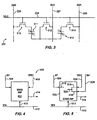
- FIG. 3 An exemplary dummy cell is shown in FIG. 3.
- This cell has the same structure as memory cell 100 of FIG. 1, including three transistors 310, 312, and 314, two ferroelectric capacitors 311 and 313, which are connected as described above, and which are connected into array 240 by word line 209, dummy bit lines 226 and 228, and dummy drive line 227, as described above for the corresponding elements of FIG. 1.
- the fact that there are two dummy bit lines 226 and 228 and two dummy ferroelectric capacitors 311 and 313 is an important feature of the invention.
- Dummy cell 220 operates in complementary mode: the ferroelectric states stored In capacitors 311 and 313, as well as the signals applied to bit lines 226 and 228, are complementary. That is, when the state of capacitor 311 is a logic "1", the state of capacitor 313 is a logic "0", and vice versa.
- each of cells 100, 202 - 206, as well as the other cells of array 200 not explicitly shown generally correspond to those of memory cell 100 depicted in FIG. 1, while the components and circuitry of each of the dummy cells in column 250 generally correspond to that of dummy cell 220 shown in FIG. 3. However, for the sake of simplicity, the internal detail of each of the cells is omitted in FIG. 2.
- word lines 209, 210 and the other word lines extend through arrays 200 and 240, each word line corresponding to a row of cells.
- bit lines 102 and 104, and drive line 103, as well as the other bit and drive lines extend through array 200 and, in the one-bit embodiment in which the bit lines are complementary, each complementary pair of bit lines and the corresponding drive line correspond to a column of cells.
- the word line and drive line coinciding at this cell would both have to be activated.
- word line 210 and drive line 103 are both active
- cell 203 is activated.
- cell 100 would preferably have an active drive line, but the absence of an active word line would prevent any voltage from reaching the electrodes of the capacitors in cell 100.
- the word line would be active, thus coupling the upper electrodes of the capacitors to drive line 207.
- drive line 207 would not be active, thereby preventing any disturbance of the polarization of the capacitors of cell 204.
- the deployment of transistors or other switching devices between both electrodes of the capacitors within each dummy cell and all sources of disturb voltages preferably operates to protect the capacitors against such disturb voltages, thereby enabling greater flexibility and compactness in memory circuit design without disturbing the polarization of the various capacitors in the memory cell.
- N is an integer and may equal zero. That is, there may be one dummy cell for each active cell. Preferably, N equals 3, 7, 15, or some other multiple of 2N-1. As known in the art, there may be many more rows above and/or below the rows shown, and many more columns, including both additional columns of active cells and additional columns of dummy cells.
- One advantage of the invention is that many more rows of cells may be used than in prior art memories, without significantly slowing the memory. That is because all cells in a column except the cell being addressed are disconnected from the drive line, and thus their capacitance does not add to the capacitance of the drive line.
- the capacitance of one memory cell capacitor is of the order of the capacitance of the drive line
- the length of the column can be extended by a factor approximately equal to the number of cells in a column of the prior art design. For example, if the prior art design was limited to eight rows, with the cell of the present invention, the design can use 64 rows and still have approximately the same speed.
- FIG. 4 illustrates the connection of a sense amplifier 402 into the array of FIG. 2 and the memory of FIG. 6 in the one-bit per cell mode
- FIG. 5 illustrates the connection of a sense amplifier 502 into the array of FIG. 2 and the memory of FIG. 6 in the two-bit embodiment.
- the design of sense amplifiers, such as 402 are well-known in the art and thus will not be described in detail.
- Sense amplifier 502 particularly the feature of how its reference signals on lines 516 and 518 are derived from dummy cell 220, is novel.
- Bit lines 406 and 408 in FIG. 4 represent a bit line pair, such as bit lines 102 and 104. In this embodiment, the bit lines correspond to opposite logic states.
- bit lines are connected to the two sides of sense amplifier 402 as known in the art.
- a sense amplifier enable signal, SEN carried by sense enable line 412 is applied to sense amp 402 via input 413.
- Sense enable line 412 is one of the lines making up signal lines 485 connected to signal generator 480 (FIG. 6).
- Data is output from sense amplifier 402 on data line 414 which is multiplexed to data output 435 (FIG. 6) as known in the art.
- bit line 506 corresponds to any of bit lines 102, 104, etc.
- sense amplifier 502 includes three bit line inputs, 516. 518, and 519. One bit line input 519 is connected to bit line 506. Bit line input 516 is connected to dummy bit line 226, and bit line input 518 is connected to dummy line 228. Within sense amplifier 502, the signals from the two dummy lines 226 and 228 are combined to yield a single reference signal on reference line 520, which reference signal is halfway between the signal DM0 and DM1. The connection of sense input 513, sense line 512, and data line 514 into memory 436 of FIG. 6 is as just described for the sense amplifier of FIG. 4.
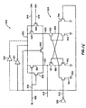
- FIG. 24 is an electrical circuit diagram illustrating a preferred embodiment of the sense amplifier of FIG. 5.
- FIG. 24 shows drivers 530, 533 and 531, which provide sense enable signals and sense amplifier 502.
- Driver 533 is optional and therefore is shown in ghost.
- Sense amplifier 502 includes N-channel transistors 541, 542, 543, 544, and 545, and P-channel transistors 551, 552, 553, 554, 555, and 556.
- the P-channel transistors may also be N-channel transistors with inverted gates.
- the bit line input 519 with signal BL is connected to the gates of transistors 553 and 554.
- the dummy bit line with signal DMO is connected to the gate of transistor 555 and the dummy bit line with signal DM1 is connected to the gate of transistor 556.
- the output of driver 530 is connected to the gate of transistors 541, 542 and 545 and the inputs of drivers 531 and 533.
- the output of drivers 533 and 531 are connected to the node 560 which connects to one source/drain of transistors 553, 554, 555, and 556.
- One source/drain of each of transistors 541 through 544 is connected to ground, such as at 560.
- the other source/drain of transistor 541 is connected to the node 562 connecting transistors 551 and 542 and to the gates of transistors 552 and 543.
- One source/drain of transistor 545 is connected to one source/drain of transistors 555, 556, and 552 and.
- the other source/drain of transistor 544 is connected to 544 is connected to the node 563 connecting transistors 552 and 543 and to the gates of transistors 551 and 542 and the other source/drain of transistor 545 is connected to one source/drain of transistors 554, 555, and 551.
- the sense amplifier 502 operates as follows. When the sense enable signal is provided on line 513, transistors 541 and 544 tum on to connect nodes 562 and 563 to ground. At the same time, driver(s) 531, 533 apply a high signal to node 560. Driver 531 provides a high signal with a relatively long period that provides sufficient time for the signal on node 560 to stabilize. Driver 533 provides a relatively fast pulse that increases the speed of node 560 going high. It is preferably used for applications that require a high operational speed. If the signal BL is higher than the combined signals DM0 and DM1, transistors 553 and 554 will turn on more than transistors 555 and 556 and node 521 will be pulled high faster.
- the circuit 503 including transistors 551, 552, 542, and 543 then acts like a conventional sense amplifier to pull the combined signals on nodes 521 and 520 to the rails. That is, if the signal on node 521 is higher than the signal on node 520, then node 521 and data line 514 is pulled high and node 520 is pulled low, and if the signal on node 521 is lower than the combined signals on nodes 521 and 520, data line 521 is pulled low.
- a separate sense amplifier 402 may be connected to each complementary pair of bit lines, or one sense amplifier may be utilized by many pairs of bit lines using transistors operated by signals from signal generator 480 (FIG. 6), via a multiplexer circuit, or in some other manner.
- a separate sense amplifier 502 may be connected between the dummy bit lines and each of the other bit lines, or one sense amplifier may be utilized with a plurality of bit lines.
- the dummy cells such as 220
- the dummy cells are driven such that the capacitors 311 and 314 are in opposite logic states.
- the specific logic states alternate, which may be every cycle, but preferably the states are changed less often, for example, every ten, twenty-five or one hundred cycles, depending on the ferroelectric material. That is, if capacitor 311 is in a logic "0" state and capacitor 314 is in a logic "1" state for one cycle series, in the next series of cycles capacitor 311 is placed in a logic "1” state and capacitor 314 is placed in a logic "0” state. This prevents the capacitors from imprinting and/or fatiguing, and improves the matching of the dummy cell tremendously.
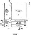
- FIG. 6 is a block diagram illustrating an exemplary integrated circuit memory 436 in which memory portion 100 is a part, and in which memory arrays, such as 200 and 240, according to the invention are utilized.
- memory portion 100 is a part
- memory arrays such as 200 and 240
- FIG. 6 is a block diagram illustrating an exemplary integrated circuit memory 436 in which memory portion 100 is a part, and in which memory arrays, such as 200 and 240, according to the invention are utilized.
- the embodiment shown is for a 16K X 1 FeRAM; however, the invention may be utilized in a wide variety of sizes and types of memories, including, but not limited to, those in which the addresses are not multiplexed, such as flash or SRAM type memories.
- there are seven address input lines 438 which connect through Control Logic section 480 and lines 439 to the X decode section 441.
- X decoder 441 is connected to a 128 X 128 memory cell array 445 via 128 lines 446, which comprise the word lines, such as 252 and 253 (FIG. 2), and the group select lines 940 and 942 (FIG. 20).
- Three other address lines 438 are decoded via Control Logic 480 to generate 8 Y select lines 486 to drive Y multiplexer 478, which drives the bit and drive lines 447, such as 102 - 104 and 226 - 228 (FIGS. 2 and 3).
- Control Logic signal generator 480 is connected to the sense amplifier and data-out multiplexer circuit 479 via lines 485. These lines provide the SEN signal discussed in connection with FIG. 4, the CH and GR SEL signals discussed below in connection with FIGS.
- DATA bus 435 is a bi-directional sixteen bit bus connected to the sense amplifier and data-out multiplexer 479 and providing a sixteen bit data input into the memory.
- X Decoder signals A 0 through As and Y Decoder signals A 7 through A 9 are latched, buffered, and decoded y Control Logic 480 and passed to X decoder 441 and two-way Y multiplexer 478, respectively.
- X decoder 441 decodes the address signals and places the word line signals, such as the WLO and WL1 signals discussed above, on one of word lines 446; generally a signal is placed on the word line of the cell that is addressed.
- the Sense Amplifiers and IO Transceiver circuit 479 includes sense amplifiers, such as 402 and 502 (FIGS. 4 and 5) which are located along lines 447 to sense and amplify the signals on the selected lines, and the IO transceiver in circuit 479 drives and receives data from data line 435.
- the various components of memory 436 in FIG. 6 are shown only as an exemplary embodiment to illustrate how the invention is used. However, there are literally hundreds of memory designs in which the invention may be used, and different designs place the various components in different locations, may not use some ot the components, or may use other components.
- the sense amplifiers are placed at the midpoint of lines 447, at the same end as the line drivers, or some other place in the circuit.
- signal generator 480 and X decoder and word line driver circuit may be combined into a single-signal generation unit.
- the circuitry of the various components of memory 436 except as discussed elsewhere herein, is known in the art of integrated circuit memory design, and will not be further discussed herein. Other logic required or useful to carry out the functions outlined above, as well as other known memory functions, is also included in memory 436 but is not shown or discussed, as it is not directly applicable to the invention.
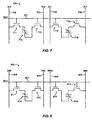
- FIG. 7 is an electrical schematic diagram of an alternative memory cell 700 according to the invention.
- This structure includes four transistors 711, 713, 714, and 716 and two ferroelectric capacitors 712 and 715.
- Transistors 711, 713 and capacitor 712 are connected to bit line 706 and drive line 707 in the same way as transistors 105 and 107 and capacitor 106 are connected to word line 101, bit line 102 and drive line 103 (FIG. 1), and transistors 714 and 716 and capacitor 715 are connected to word line 701, bit line 709, and drive line 708 in the same was as transistors 107 and 109 and capacitor 108 are connected to word line 101, bit line 104, and drive line 103.
- cell 700 can be programmed as a single bit cell with capacitors 712 and 715 in complementary states, or as a two-bit cell.
- This structure like the structure of cell 100 of FIG. 1, is excellent in a high noise environment, such as embedded memory, since the ferroelectric capacitors 712, 715 are completely isolated except when they are being addressed.
- the write cycle is approximately half of the write cycle of cell 100; thus, a memory with a cell 700 is extremely fast.
- FIG. 8 shows a dummy cell 800 in which transistors 811, 813, 814, and 816 and capacitors 812 and 815 are connected to bit lines 806 and 809, word line 801, and drive lines 807 and 808 just as the corresponding transistors and capacitors are connected in cell 700.
- dummy lines 807 and 808 always have complementary signals, as do bit lines 806 and 809.
- Sense amplifiers 402 (FIG. 4) and 502 (FIG. 5) are preferably used with the one-bit embodiment of cell 700 and the two-bit embodiment of cell 700 as described above for cell 100 of FIG. 1.
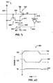
- Drive circuit 900 includes two transistors 902 and 904 and a capacitor 906.
- Transistor 902 has an inverted gate.
- Transistor 902 may also be a P-channel transistor while transistor 904 is an N-channel transistor.
- Capacitor 906 may be a ferroelectric capacitor or a conventional linear capacitor.
- the inverted gate of transistor 902 is connected to "charge" line 908.
- One source/drain of transistor 902 is connected to Vdd, while the other source drain is connected to electrode 915 of capacitor 906, which is preferably the lower electrode.
- the other electrode 916 of capacitor 906 is connected to ground 914 via line 921.
- the second embodiment includes a buffer amplifier 917.
- the input of buffer 917 is connected to charge line 908 and the output is connected to electrode 916.
- Node 911 between transistor 902 and electrode 915 is also connected to bit line 907 through transistor 904, the gate of which is connected to charge line 908.
- P channel transistor 902 can be replaced with a P/NB transmission gate or any gating element which will turn ON when CH is low.
- the N channel transistor 904 can also be replaced with a P/N transmission gate or any gating element which will turn ON when CH is high.
- a timing diagram 920 showing the operation of bit line driver 900 is shown in FIG. 10.
- the CH signal on the charge line is low, which means that transistor 902 is on and transistor 904 is off.
- electrode 915 is pulled high, and the LE signal, which represents the voltage state of this electrode, is high.
- the CH signal on the charge line goes high, which turns off transistor 902 and turns on transistor 904, which permits the positive charge on electrode 915 to be dumped onto bit line 907, causing the voltage BL on the bit line to rise a small amount.
- capacitor 915 is selected so that the voltage the bit line rises to is one-third or less of the high voltage source of the memory, i.e., the Vdd voltage. More preferably, it is one-fourth or less of the memory high voltage.
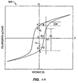
- FIG. 11 is a ferroelectric hysteresis curve 925 plotting polarizability P of a ferroelectric capacitor, such as 106, versus voltage.
- a ferroelectric capacitor such as 106
- V the voltage
- FIG. 11 illustrates how the different steepness of the hysteresis curve leads to a robust sensing scheme. If a small charge is applied to the ferroelectric capacitor, there will be a large difference in the voltage generated on the capacitor depending on whether the capacitor is in the "logic 1" state or the "logic 0" state. The voltage developed if the capacitor is in the state “A” will be much larger than the voltage developed if the capacitor is in the state "C". The voltage developed will not be enough to change the state of the ferroelectric capacitor but the voltage difference can be easily sensed by stat-of-the-art sense amplifiers. After sensing, the charge can be quickly removed. A write back operation may optionally be used if an extremely robust system is desired, depending on design requirements.
- the ferroelectric capacitor will dump a charge on the bit line.
- the difference between the charge dumped in the "logic 1" state and the charge dumped in the "logic 0" state is QL-QK.
- This large charge difference QL-QK, between the two different states of the capacitor can be easily sensed by state-of-the-art sense amplifiers. After the sense amplifier detects the state, a write back operation may or may not be performed depending on the design requirements.
- the hysteresis curve on subsequent cycles after the first also shifts, so that the capacitor in the logic "1" state always absorbs less charge than the capacitor in the logic "0" state.
- the above also explains why, for a robust system, it is desirable to have a rewrite cycle even though the capacitor is not switched in the SNDRO read methods described above.
- the rewrite cycle returns the capacitors to the states A and C, respectively; thus, the relaxation of the capacitor does not impact the performance of the capacitor.
- Array 930 includes several levels of bit lines.
- the top level bit line 932 Is one of lines 447 of memory 436 (FIG. 6). That is, it is closer to Y Multiplexer 478.
- Each top level bit line, such as 932 has multiple groups (947, 948) of two second level bit lines 934 and 936 associated with it.
- the extension of the bit lines such as 932, 934 and 936 at the top and bottom of the figure is Intended to indicate the preferred presence of multiple groups of second level bit lines.
- the number of second level bit lines will depend on layout and circuit design considerations which can be different for different implementation strategies.
- Each second level bit line 934, 936 is connected to the top level bit line 932 through a transistor 938 and 939, respectively.
- the gate of transistor 938 is connected to a first group select line 940, while the gate of transistor 939 is connected to a second group select line 942.
- the top left memory cell or array 930 is also the top left memory cell of arrays 200, 240, and have numbered the elements the same.
- a group select line and a word line corresponding to the cell must be active.
- the GRSEL1 signal must be high turning on transistor 938 and connecting second level bit line 934 to top level bit line 932, and word line 101 must be high turning on transistors 105, 107, and 109.
- GRSEL1 is low and GRSEL2 is high.
- Each second level bit line such as 934, is connected to a small number of memory cells, e.g., 8, 16, etc.
- the total bit line capacitance is the sum of the top level bit line capacitance and the second level bit line capacitance. Since only one second level bit line is connected to the top level bit line when accessing a cell, the capacitances of the other second level bit lines do not affect the total bit line capacitance. Thus, the partitioning of the bit lines significantly lowers the bit line capacitance, which significantly increases the speed at which the bit line will come up to full voltage, which speeds up the memory.
- Array 930 also includes several levels of drive lines.
- the top level drive line 941 is one of lines 447 of memory 436 (FIG. 6). That is, it is closer to Y Multiplexer 478.
- Each top level drive line, such as 941 has multiple groups of two second level drive lines 945 and 946 associated with it.
- the extension of the drive lines such as 941, 945 and 946 at the top and bottom of the figure is intended to indicate the preferred presence of multiple groups of second level drive lines. Again, the number of second level drive lines will depend on layout and circuit design considerations.
- Each second level drive line 945, 946 is connected to the top level drive line 941 through a transistor 943 and 944, respectively.
- each second level drive line such as 943
- the total drive line capacitance is the sum of the top level drive line capacitance and the second level drive line capacitance. Since only one second level drive line is connected to the top level drive line when accessing a cell, the capacitances of the other second level drive lines do not affect the total drive line capacitance.
- the partitioning of the drive lines significantly lowers the drive line capacitance, which significantly increases the speed at which the drive line will come up to full voltage, which speeds up the memory.
- bit lines and drive lines are partioned, in other embodiments only the bit lines or only the drive lines may be partioned. Additional levels below the second level may exist also.
- the important aspect is that there is a hierarchy of bit lines and/or drive lines, with each top level line connecting with multiple second level lines through transistors, each second level connecting line connecting with multiple third level lines through transistors, etc.
- Word lines may also be partioned in a similar manner to the bit and drive lines.
- cell 100 has an extra transistor as compared to, for example, conventional DRAM designs, it would seem that it would be somewhat less dense than a comparable complementary mode DRAM design, or a comparable DRAM design using dummy cells.
- density of the cell portion of the memory is somewhat more than conventional designs sometimes labeled as 1T/1C, the advantages of isolation and low power lead to an overall low density when the support structures that every memory must have are considered.
- the capacitors that are not addressed are isolated and their capacitance does not contribute to the drive and bit line capacitance, the arrays may be made much larger than previous arrays of ferroelectric memories, without having huge bit line and drive line drivers, and without having a plate line driver for each row of cells, as in some prior art memories.
- the supporting structure is much smaller, the overall memory density is smaller. As compared to DRAMS, refresh circuitry is not required because the memory is non-volatile. Moreover, the drive line located between the bit lines permits an efficient design of the memory, and at the same time reduces cross-talk between the bit lines, which allows all the elements of the array to be more compact.
- the memory according to the invention also uses much less power than prior art designs.
- many non-addressed cells were continually being powered up. This is wasteful of power and is eliminated in the memory according to the invention.
- the reduced capacitance also greatly enhances the speed of the memory.
- the reduced capacitance means that the time for the voltage lines to stabilize is smaller, and the cycle time is also correspondingly smaller.
- the isolation also leads to less noise, and completely eliminates disturb to a non-selected memory cell due to other memory cells being written to or read. This lower noise and elimination of many of the sources of disturb permits a reliable SNDRO read function, which is extremely fast.
- FIG. 21 is an electrical circuit diagram of a portion 950 of a memory array in which each drive line 955 and drive line transistor 956 is associated with a pair of two transistor, two ferroelectric capacitor memory cells 953 and 954.
- a single drive line 955 is connected to each of capacitors 957, 958, 959 and 960.
- the circuit Is the same as circuit 100 of FIG. 1.
- Circuit 950 may be considered as a single two-bit cell 951 having four capacitors and five transistors, or as two one-bit cells 953 and 954 with a drive line 955 connected to the two cells through a drive transistor.
- FIG. 14 is an electrical circuit diagram of a portion 966 of a memory array that is the same as array 950 except that drive line 968 is located between bit line pairs 969, 970 and 971, 972.
- This embodiment may also be considered as a single two-bit cell or two one-bit cells. This embodiment is more preferred than the embodiment of FIG. 13, since it has less noise and the layout is more balanced and efficient.
- FIG. 15 shows another embodiment of a portion 980 of a memory array that has the same structure as the embodiment of FIG. 13, except that bit line pairs 982, 983 and 984, 985 are not complementary, capacitor 988 is a dummy capacitor, and bit line 985 is a dummy bit line.
- Circuit 980 can be considered to be a single three-bit cell 989 or three one-bit cells 990, 991, and 992.
- FIGS. 13 - 15 are more dense and faster than any prior art ferroelectric memories, but are a bit slower than the previous embodiments, and use more power. If one attempts to use more than four capacitors attached to a single drive line, the drivers and support circuitry become so large and the speed decreases so much that most of the advantages of the invention are lost. Layout efficiencies are also lost.
- ferroelectric memory in which the ferroelectric elements are capacitors.
- ferroelectric elements are ferroelectric FETs or other ferroelectric elements. See, for example, United States Patent No. 6,339,238 issued January 15, 2002 to Lim et al., which is incorporated herein by reference as though fully disclosed herein.
- Many of the elements, such as the structure in which cells are completely isolated, are also applicable to DRAMS.
Landscapes
- Engineering & Computer Science (AREA)
- Computer Hardware Design (AREA)
- Dram (AREA)
- Semiconductor Memories (AREA)
- Inorganic Insulating Materials (AREA)
Claims (11)
- Ferroelektrischer, nicht flüchtiger Speicher (436), der aufweist: eine Vielzahl (248, 249) von Paaren aus parallelen Bitleitungen (102, 104; 706, 709), eine Vielzahl von Treiberleitungen (103; 707, 708) parallel zu den Bitleitungen, eine Wortleitung (101, 701) senkrecht zu den Bitleitungspaaren und den Treiberleitungen und eine Vielzahl von Speicherzellen (100, 202 - 206, 700), wobei jeder Speicherzelle eines der Paare der Bitleitungen (102, 104; 706, 709) und eine der Treiberleitungen (103; 707, 708) zugeordnet ist, wobei jede Speicherzelle (100, 202 - 206, 700) umfaßt: einen ersten ferroelektrischen Kondensator (106, 712) mit eine ersten Elektrode (126) und einer zweiten Elektrode (125), einen zweiten ferroelektrischen Kondensator (108, 715) mit einer ersten Elektrode (134) und einer zweiten Elektrode (133), einen ersten Transistor (105, 711) mit einem Gatter (123) und einen zweiten Transistor (109, 716) mit einem Gatter (136); wobei in jeder der Speicherzellen der erste Transistor (105, 711) zwischen die erste Elektrode (126) des ersten Kondensators (106, 712) und eine (102, 706) der Bitleitungen in dem zugeordnen Bitleitungspaar geschaltet ist und der zweite Transistor (109, 716) zwischen die erste Elektrode (134) des zweiten Kondensators (108, 715) und die andere (104, 709) der Bitleitungen in dem zugeordneten Bitleitungspaar geschaltet ist, und die Gatter (123, 126) des ersten und zweiten Transistors (105, 109; 711, 716) mit der Wortleitung (101, 701) verbunden sind; wobei der Speicher gekennzeichnet ist durch einen Treiberleitungs-Transistor (107, 713, 714), der jeder der Treiberleitungen (103; 707, 708) zugewiesen ist, wobei der Treiberleitungs-Transistor (107, 713) ein Gatter (128) umfaßt, wobei jede der Treiberleitungen (103; 707, 708) mit der zweiten Elektrode (125, 133) des ersten und zweiten ferroelektrischen Kondensators (106, 108; 712, 715) in der Speicherzelle (100, 202 - 206, 700), der der Treiberleitung zugewiesen ist (103; 707, 708) über den Treiberleitungs-Transistor (107; 713, 714) verbunden ist, wobei jede der Treiberleitungen (103; 707, 708) mit zwei oder weniger der Speicherzellen (100, 202 - 206, 700) verbunden ist; und wobei das Gatter (128) des Treiberleitungs-Transistors (107, 713, 714) mit der Wortleitung (101, 701) verbunden ist.
- Ferroelektrischer, nicht flüchtiger Speicher nach Anspruch 1, bei dem die Speicherzellen (10, 202 - 206) in Reihen (252, 253) parallel zu den Wortleitungen (101) und Spalten (248, 249) parallel zu den Bit-(102, 104) und Treiberleitungen (103) angeordnet sind, dadurch gekennzeichnet, daß jede der Treiberleitungen (103) mit der zweiten Elektrode (125) des ersten Kondensators (106) und der zweiten Elektrode (133) des zweiten Kondensators (108) in nur einer der Speicherzellen in einer Reihe (252, 253) aus Speicherzellen (100, 202 - 206) verbunden ist.
- Ferroelektrischer, nicht flüchtiger Speicher nach Anspruch 1, bei dem es eine der Treiberleitungen (103) gibt, die jeder der Zellen (100, 202 - 206) zugeordnet ist, und sich die Treiberleitung (103) zwischen den Bitleitungen (102, 104) in dem Bitleitungspaar, das der Zelle zugeordnet ist, der die Treiberleitung (103) zugeordnet ist, befindet.
- Ferroelektrischer, nicht flüchtiger Speicher nach Anspruch 1, bei dem die Speicherzellen (953, 954) in Reihen parallel zu den Wortleitungen und Spalten parallel zu den Bitleitungen (969, 970, 971, 972) und den Treiberleitungen (955, 968) angeordnet sind, dadurch gekennzeichnet, daß jede der Treiberleitungen (955, 968) mit der zweiten Elektrode des ersten Kondensators und der zweiten Elektrode des zweiten Kondensators in zwei der Speicherzellen (953, 954) in einer Reihe aus Speicherzellen verbunden ist.
- Ferroelektrischer, nicht flüchtiger Speicher nach Anspruch 4, bei dem die Treiberleitung (968) sich zwischen den beiden Zellen befindet.
- Ferroelektrischer, nicht flüchtiger Speicher nach Anspruch 1, bei dem die Bitleitungen (406, 408) komplementär sind und jede der Speicherzellen eine Ein-Bit-Speicherzelle ist.
- Ferroelektrischer, nicht flüchtiger Speicher nach Anspruch 1, bei dem einer der Kondensatoren ein ferroelektrischer Dummy-Kondensator (998) ist und die Bitleitung, die mit dem ferroelektrischen Dummy-Kondensator (988) verbunden ist, eine Dummy-Bitleitung (985) ist.
- Ferroelektrischer Speicher nach Anspruch 1, bei dem die Bitleitungen höchstrangige Bitleitungen (932) sind und es eine Vielzahl der Speicherzellen gibt, die in eine erste Gruppe (947) und eine zweite Gruppe (948) aufgeteilt sind, wobei der Speicher weiter einen Transistor (938) zum Auswählen einer ersten Gruppe mit einem Gatter, einen Transistor (939) zum Auswählen einer zweiten Gruppe mit einem Gatter, eine Auswahlleitung (940) für die erste Gruppe, eine Auswahlleitung (942) für die zweite Gruppe, eine erste zweitrangige Bitleitung (934) und eine zweite zweitrangige Bitleitung (936) umfaßt und bei dem der Transistor (938) zum Auswählen einer ersten Gruppe zwischen die höchstrangige Bitleitung (932) und die erste zweitrangige Bitleitung (934) geschaltet ist, wobei der Transistor (939) zum Auswählen der zweiten Gruppe zwischen die höchstrangige Bitleitung (932) und die zweite zweitrangige Bitleitung (936) geschaltet ist, wobei die Auswahlleitung (940) für die erste Gruppe mit dem Gatter des Transistors (938) zum Auswählen der ersten Gruppe verbunden ist und die Auswahlleitung (942) für die zweite Gruppe mit dem Gatter des Transistors (939) zum Auswählen der zweiten Gruppe verbunden ist.
- Ferroelektrischer Speicher nach Anspruch 8 und weiter eine Bitleitungs-Treiberschaltung (900) zum Treiben der Bitleitung (907) auf eine Spannung, die ein Drittel oder weniger der Hoch-Spannung des Speichers beträgt, umfassend.
- Ferroelektrischer, nicht flüchtiger Speicher nach Anspruch 1, bei dem jede der Speicherzellen eine Zwei-Bit-Speicherzelle ist.
- Ferroelektrischer, nicht flüchtiger Speicher nach Anspruch 10, bei dem einer der Kondensatoren ein ferroelektrischer Dummy-Kondensator ist und die Bitleitung, die mit dem ferroelektrischen Dummy-Kondensator verbunden ist, eine Dummy-Bitleitung (226, 228) ist.
Applications Claiming Priority (3)
| Application Number | Priority Date | Filing Date | Title |
|---|---|---|---|
| US139426 | 2002-05-06 | ||
| US10/139,426 US6809949B2 (en) | 2002-05-06 | 2002-05-06 | Ferroelectric memory |
| PCT/US2003/014015 WO2003096352A2 (en) | 2002-05-06 | 2003-05-05 | Ferroelectric memory |
Publications (2)
| Publication Number | Publication Date |
|---|---|
| EP1502265A2 EP1502265A2 (de) | 2005-02-02 |
| EP1502265B1 true EP1502265B1 (de) | 2006-11-02 |
Family
ID=29269544
Family Applications (1)
| Application Number | Title | Priority Date | Filing Date |
|---|---|---|---|
| EP03722013A Expired - Lifetime EP1502265B1 (de) | 2002-05-06 | 2003-05-05 | Ferroelektrischer speicher |
Country Status (10)
| Country | Link |
|---|---|
| US (2) | US6809949B2 (de) |
| EP (1) | EP1502265B1 (de) |
| JP (1) | JP2005530283A (de) |
| KR (1) | KR20050025176A (de) |
| CN (1) | CN100533590C (de) |
| AT (1) | ATE344525T1 (de) |
| AU (1) | AU2003225292A1 (de) |
| DE (1) | DE60309461T2 (de) |
| TW (1) | TWI301271B (de) |
| WO (1) | WO2003096352A2 (de) |
Families Citing this family (65)
| Publication number | Priority date | Publication date | Assignee | Title |
|---|---|---|---|---|
| US6822891B1 (en) * | 2003-06-16 | 2004-11-23 | Kabushiki Kaisha Toshiba | Ferroelectric memory device |
| US7193880B2 (en) * | 2004-06-14 | 2007-03-20 | Texas Instruments Incorporated | Plateline voltage pulsing to reduce storage node disturbance in ferroelectric memory |
| JP3970259B2 (ja) * | 2003-09-11 | 2007-09-05 | 三洋電機株式会社 | メモリ |
| JP4074279B2 (ja) * | 2003-09-22 | 2008-04-09 | 株式会社東芝 | 半導体集積回路装置、デジタルカメラ、デジタルビデオカメラ、コンピュータシステム、携帯コンピュータシステム、論理可変lsi装置、icカード、ナビゲーションシステム、ロボット、画像表示装置、光ディスク記憶装置 |
| KR100583112B1 (ko) * | 2003-11-27 | 2006-05-23 | 주식회사 하이닉스반도체 | 싱글엔디드 센싱 구조를 갖는 불휘발성 강유전체 메모리장치 |
| US7099179B2 (en) * | 2003-12-22 | 2006-08-29 | Unity Semiconductor Corporation | Conductive memory array having page mode and burst mode write capability |
| US7009864B2 (en) * | 2003-12-29 | 2006-03-07 | Texas Instruments Incorporated | Zero cancellation scheme to reduce plateline voltage in ferroelectric memory |
| US20050174841A1 (en) * | 2004-02-05 | 2005-08-11 | Iota Technology, Inc. | Electronic memory with tri-level cell pair |
| US7352619B2 (en) * | 2004-02-05 | 2008-04-01 | Iota Technology, Inc. | Electronic memory with binary storage elements |
| US7133304B2 (en) * | 2004-03-22 | 2006-11-07 | Texas Instruments Incorporated | Method and apparatus to reduce storage node disturbance in ferroelectric memory |
| NO322040B1 (no) * | 2004-04-15 | 2006-08-07 | Thin Film Electronics Asa | Bimodal drift av ferroelektriske og elektrete minneceller og innretninger |
| US6970371B1 (en) * | 2004-05-17 | 2005-11-29 | Texas Instruments Incorporated | Reference generator system and methods for reading ferroelectric memory cells using reduced bitline voltages |
| US20050274396A1 (en) * | 2004-06-09 | 2005-12-15 | Hong Shih | Methods for wet cleaning quartz surfaces of components for plasma processing chambers |
| US7472309B2 (en) * | 2004-12-22 | 2008-12-30 | Intel Corporation | Methods and apparatus to write a file to a nonvolatile memory |
| EP1833091A4 (de) * | 2004-12-28 | 2008-08-13 | Spansion Llc | Halbleitereinrichtung und betriebssteuerverfahren dafür |
| JP4912016B2 (ja) * | 2005-05-23 | 2012-04-04 | ルネサスエレクトロニクス株式会社 | 半導体記憶装置 |
| US20070190670A1 (en) * | 2006-02-10 | 2007-08-16 | Forest Carl A | Method of making ferroelectric and dielectric layered superlattice materials and memories utilizing same |
| US7561458B2 (en) * | 2006-12-26 | 2009-07-14 | Texas Instruments Incorporated | Ferroelectric memory array for implementing a zero cancellation scheme to reduce plateline voltage in ferroelectric memory |
| KR100866751B1 (ko) * | 2006-12-27 | 2008-11-03 | 주식회사 하이닉스반도체 | 강유전체 소자를 적용한 반도체 메모리 장치 및 그리프레쉬 방법 |
| KR100866705B1 (ko) * | 2007-07-04 | 2008-11-03 | 주식회사 하이닉스반도체 | 강유전체 소자를 적용한 반도체 메모리 장치 |
| KR100849794B1 (ko) * | 2007-07-04 | 2008-07-31 | 주식회사 하이닉스반도체 | 강유전체 소자를 적용한 반도체 메모리 장치 |
| JP2009043307A (ja) * | 2007-08-06 | 2009-02-26 | Toshiba Corp | 半導体記憶装置 |
| US7920404B2 (en) * | 2007-12-31 | 2011-04-05 | Texas Instruments Incorporated | Ferroelectric memory devices with partitioned platelines |
| US8130559B1 (en) | 2008-08-06 | 2012-03-06 | Altera Corporation | MEMS switching device and conductive bridge device based circuits |
| US7898837B2 (en) * | 2009-07-22 | 2011-03-01 | Texas Instruments Incorporated | F-SRAM power-off operation |
| CN101819811B (zh) * | 2010-03-31 | 2013-10-16 | 清华大学 | 三值铁电存储器电路 |
| JP6030298B2 (ja) * | 2010-12-28 | 2016-11-24 | 株式会社半導体エネルギー研究所 | 緩衝記憶装置及び信号処理回路 |
| JP5673414B2 (ja) * | 2011-07-20 | 2015-02-18 | 富士通セミコンダクター株式会社 | 半導体装置の製造方法 |
| US8756558B2 (en) * | 2012-03-30 | 2014-06-17 | Texas Instruments Incorporated | FRAM compiler and layout |
| US20140029326A1 (en) * | 2012-07-26 | 2014-01-30 | Texas Instruments Incorporated | Ferroelectric random access memory with a non-destructive read |
| KR102330412B1 (ko) * | 2014-04-25 | 2021-11-25 | 가부시키가이샤 한도오따이 에네루기 켄큐쇼 | 반도체 장치, 전자 부품, 및 전자 기기 |
| US9767879B2 (en) * | 2015-02-17 | 2017-09-19 | Texas Instruments Incorporated | Setting of reference voltage for data sensing in ferroelectric memories |
| US9460770B1 (en) | 2015-09-01 | 2016-10-04 | Micron Technology, Inc. | Methods of operating ferroelectric memory cells, and related ferroelectric memory cells |
| US9443576B1 (en) * | 2015-11-09 | 2016-09-13 | Microsoft Technology Licensing, Llc | Josephson magnetic random access memory with an inductive-shunt |
| US9786347B1 (en) * | 2016-03-16 | 2017-10-10 | Micron Technology, Inc. | Cell-specific reference generation and sensing |
| US9721639B1 (en) * | 2016-06-21 | 2017-08-01 | Micron Technology, Inc. | Memory cell imprint avoidance |
| CN109690680B (zh) | 2016-08-31 | 2023-07-21 | 美光科技公司 | 包含二晶体管一电容器的存储器及用于存取所述存储器的设备与方法 |
| KR102369776B1 (ko) | 2016-08-31 | 2022-03-03 | 마이크론 테크놀로지, 인크. | 강유전 메모리 셀 |
| WO2018044487A1 (en) * | 2016-08-31 | 2018-03-08 | Micron Technology, Inc. | Apparatuses and methods including ferroelectric memory and for accessing ferroelectric memory |
| EP3507805B1 (de) | 2016-08-31 | 2025-10-01 | Micron Technology, Inc. | Vorrichtungen und verfahren mit ferroelektrischem speicher und zum betrieb von ferroelektrischem speicher |
| US10418084B2 (en) | 2017-02-07 | 2019-09-17 | Micron Technology, Inc. | Pre-writing memory cells of an array |
| JP6915372B2 (ja) * | 2017-05-16 | 2021-08-04 | 富士通株式会社 | メモリセル、メモリモジュール、情報処理装置およびメモリセルのエラー訂正方法 |
| US10867675B2 (en) | 2017-07-13 | 2020-12-15 | Micron Technology, Inc. | Apparatuses and methods for memory including ferroelectric memory cells and dielectric memory cells |
| US10163480B1 (en) | 2017-07-27 | 2018-12-25 | Micron Technology, Inc. | Periphery fill and localized capacitance |
| US10032496B1 (en) | 2017-07-27 | 2018-07-24 | Micron Technology, Inc. | Variable filter capacitance |
| US10410721B2 (en) * | 2017-11-22 | 2019-09-10 | Micron Technology, Inc. | Pulsed integrator and memory techniques |
| JP7159199B2 (ja) * | 2017-12-04 | 2022-10-24 | ソニーセミコンダクタソリューションズ株式会社 | 半導体記憶装置、電子機器及び情報の読み出し方法 |
| US10622050B2 (en) * | 2018-05-09 | 2020-04-14 | Micron Technology, Inc. | Ferroelectric memory plate power reduction |
| US10825513B2 (en) * | 2018-06-26 | 2020-11-03 | Sandisk Technologies Llc | Parasitic noise control during sense operations |
| US10998025B2 (en) | 2019-02-27 | 2021-05-04 | Kepler Computing, Inc. | High-density low voltage non-volatile differential memory bit-cell with shared plate-line |
| US11476261B2 (en) | 2019-02-27 | 2022-10-18 | Kepler Computing Inc. | High-density low voltage non-volatile memory with unidirectional plate-line and bit-line and pillar capacitor |
| US11062763B2 (en) * | 2019-04-09 | 2021-07-13 | Micron Technology, Inc. | Memory array with multiplexed digit lines |
| CN110428857B (zh) * | 2019-07-09 | 2021-09-24 | 清华大学 | 一种基于滞回特性器件的存储器 |
| CN111292782B (zh) * | 2019-10-21 | 2021-11-02 | 北京潼荔科技有限公司 | 非易失性随机存取存储器及存取方法 |
| US11729989B2 (en) * | 2020-01-06 | 2023-08-15 | Iu-Meng Tom Ho | Depletion mode ferroelectric transistors |
| US11527277B1 (en) | 2021-06-04 | 2022-12-13 | Kepler Computing Inc. | High-density low voltage ferroelectric memory bit-cell |
| US12112792B2 (en) * | 2021-08-10 | 2024-10-08 | Micron Technology, Inc. | Memory device for wafer-on-wafer formed memory and logic |
| US11729995B1 (en) | 2021-11-01 | 2023-08-15 | Kepler Computing Inc. | Common mode compensation for non-linear polar material 1TnC memory bit-cell |
| US11482270B1 (en) * | 2021-11-17 | 2022-10-25 | Kepler Computing Inc. | Pulsing scheme for a ferroelectric memory bit-cell to minimize read or write disturb effect and refresh logic |
| US12108609B1 (en) | 2022-03-07 | 2024-10-01 | Kepler Computing Inc. | Memory bit-cell with stacked and folded planar capacitors |
| US20230395134A1 (en) | 2022-06-03 | 2023-12-07 | Kepler Computing Inc. | Write disturb mitigation for non-linear polar material based multi-capacitor bit-cell |
| US12347476B1 (en) | 2022-12-27 | 2025-07-01 | Kepler Computing Inc. | Apparatus and method to improve sensing noise margin in a non-linear polar material based bit-cell |
| US12334127B2 (en) | 2023-01-30 | 2025-06-17 | Kepler Computing Inc. | Non-linear polar material based multi-capacitor high density bit-cell |
| CN118692537B (zh) * | 2023-03-21 | 2025-09-26 | 清华大学 | 基于铁电电容的非易失内容寻址存储器、电子设备 |
| CN121096391A (zh) * | 2025-07-31 | 2025-12-09 | 上海深明奥思半导体科技有限公司 | 具有存储栅极线的2t1fc铁电存储单元及其制备方法 |
Family Cites Families (29)
| Publication number | Priority date | Publication date | Assignee | Title |
|---|---|---|---|---|
| US4873664A (en) * | 1987-02-12 | 1989-10-10 | Ramtron Corporation | Self restoring ferroelectric memory |
| US4888733A (en) * | 1988-09-12 | 1989-12-19 | Ramtron Corporation | Non-volatile memory cell and sensing method |
| US5038323A (en) * | 1990-03-06 | 1991-08-06 | The United States Of America As Represented By The Secretary Of The Navy | Non-volatile memory cell with ferroelectric capacitor having logically inactive electrode |
| US5262982A (en) | 1991-07-18 | 1993-11-16 | National Semiconductor Corporation | Nondestructive reading of a ferroelectric capacitor |
| US5666305A (en) * | 1993-03-29 | 1997-09-09 | Olympus Optical Co., Ltd. | Method of driving ferroelectric gate transistor memory cell |
| US5373463A (en) * | 1993-07-06 | 1994-12-13 | Motorola Inc. | Ferroelectric nonvolatile random access memory having drive line segments |
| US5406510A (en) * | 1993-07-15 | 1995-04-11 | Symetrix Corporation | Non-volatile memory |
| JP3218844B2 (ja) * | 1994-03-22 | 2001-10-15 | 松下電器産業株式会社 | 半導体メモリ装置 |
| DE69621293T2 (de) | 1995-08-02 | 2002-12-12 | Matsushita Electric Industrial Co., Ltd. | Ferroelektrische Speichervorrichtung |
| US5598366A (en) * | 1995-08-16 | 1997-01-28 | Ramtron International Corporation | Ferroelectric nonvolatile random access memory utilizing self-bootstrapping plate line segment drivers |
| SG79200A1 (en) | 1995-08-21 | 2001-03-20 | Matsushita Electric Industrial Co Ltd | Ferroelectric memory devices and method for testing them |
| US5969979A (en) * | 1996-03-25 | 1999-10-19 | Matsushita Electronics Corporation | Ferroelectric memory device |
| US5737260A (en) * | 1996-03-27 | 1998-04-07 | Sharp Kabushiki Kaisha | Dual mode ferroelectric memory reference scheme |
| KR100206713B1 (ko) | 1996-10-09 | 1999-07-01 | 윤종용 | 강유전체 메모리 장치에서의 비파괴적 억세싱 방법 및 그 억세싱 회로 |
| US5966318A (en) * | 1996-12-17 | 1999-10-12 | Raytheon Company | Nondestructive readout memory utilizing ferroelectric capacitors isolated from bitlines by buffer amplifiers |
| JP3495905B2 (ja) | 1998-02-19 | 2004-02-09 | シャープ株式会社 | 半導体記憶装置 |
| KR100268947B1 (ko) | 1998-04-03 | 2000-10-16 | 김영환 | 비휘발성 강유전체 메모리 및 그의 제어회로 |
| US6215692B1 (en) * | 1998-05-13 | 2001-04-10 | Hyundai Electronics Industries Co., Ltd. | Non-volatile ferroelectric memory |
| KR100281125B1 (ko) | 1998-12-29 | 2001-03-02 | 김영환 | 비휘발성 강유전체 메모리장치 |
| KR100363102B1 (ko) * | 1998-07-15 | 2003-02-19 | 주식회사 하이닉스반도체 | 강유전체 메모리 |
| US5995407A (en) * | 1998-10-13 | 1999-11-30 | Celis Semiconductor Corporation | Self-referencing ferroelectric memory |
| US6147895A (en) * | 1999-06-04 | 2000-11-14 | Celis Semiconductor Corporation | Ferroelectric memory with two ferroelectric capacitors in memory cell and method of operating same |
| US6330180B2 (en) * | 2000-03-24 | 2001-12-11 | Fujitsu Limited | Semiconductor memory device with reduced power consumption and with reduced test time |
| JP2001319472A (ja) * | 2000-05-10 | 2001-11-16 | Toshiba Corp | 半導体記憶装置 |
| ATE314721T1 (de) * | 2000-09-25 | 2006-01-15 | Symetrix Corp | Ferro-elektrischer speicher und sein betriebsverfahren |
| JP2002109875A (ja) * | 2000-09-29 | 2002-04-12 | Nec Corp | 強誘電体容量を用いたシャドーramセル及び不揮発性メモリ装置並びにその制御方法 |
| KR100428652B1 (ko) * | 2001-03-28 | 2004-04-29 | 주식회사 하이닉스반도체 | 인접 셀간에 셀 플레이트를 공유하는 강유전체 메모리 소자 |
| US6522570B1 (en) * | 2001-12-13 | 2003-02-18 | Micron Technology, Inc. | System and method for inhibiting imprinting of capacitor structures of a memory |
| US6873536B2 (en) * | 2002-04-19 | 2005-03-29 | Texas Instruments Incorporated | Shared data buffer in FeRAM utilizing word line direction segmentation |
-
2002
- 2002-05-06 US US10/139,426 patent/US6809949B2/en not_active Expired - Lifetime
-
2003
- 2003-05-05 KR KR1020047017893A patent/KR20050025176A/ko not_active Withdrawn
- 2003-05-05 EP EP03722013A patent/EP1502265B1/de not_active Expired - Lifetime
- 2003-05-05 WO PCT/US2003/014015 patent/WO2003096352A2/en not_active Ceased
- 2003-05-05 AU AU2003225292A patent/AU2003225292A1/en not_active Abandoned
- 2003-05-05 JP JP2004504239A patent/JP2005530283A/ja active Pending
- 2003-05-05 DE DE60309461T patent/DE60309461T2/de not_active Expired - Fee Related
- 2003-05-05 AT AT03722013T patent/ATE344525T1/de not_active IP Right Cessation
- 2003-05-05 CN CNB038159813A patent/CN100533590C/zh not_active Expired - Fee Related
- 2003-05-06 TW TW092112308A patent/TWI301271B/zh not_active IP Right Cessation
- 2003-11-10 US US10/704,847 patent/US7212427B2/en not_active Expired - Lifetime
Also Published As
| Publication number | Publication date |
|---|---|
| AU2003225292A8 (en) | 2003-11-11 |
| JP2005530283A (ja) | 2005-10-06 |
| CN100533590C (zh) | 2009-08-26 |
| TWI301271B (en) | 2008-09-21 |
| KR20050025176A (ko) | 2005-03-11 |
| ATE344525T1 (de) | 2006-11-15 |
| DE60309461D1 (de) | 2006-12-14 |
| DE60309461T2 (de) | 2007-09-20 |
| US20040105296A1 (en) | 2004-06-03 |
| US7212427B2 (en) | 2007-05-01 |
| WO2003096352A3 (en) | 2004-06-24 |
| EP1502265A2 (de) | 2005-02-02 |
| CN1666293A (zh) | 2005-09-07 |
| AU2003225292A1 (en) | 2003-11-11 |
| WO2003096352A2 (en) | 2003-11-20 |
| US6809949B2 (en) | 2004-10-26 |
| US20030206430A1 (en) | 2003-11-06 |
| HK1081320A1 (zh) | 2006-05-12 |
| TW200400509A (en) | 2004-01-01 |
Similar Documents
| Publication | Publication Date | Title |
|---|---|---|
| US6809949B2 (en) | Ferroelectric memory | |
| US6147895A (en) | Ferroelectric memory with two ferroelectric capacitors in memory cell and method of operating same | |
| US6185123B1 (en) | Memory cell configuration for a 1T/1C ferroelectric memory | |
| US5373463A (en) | Ferroelectric nonvolatile random access memory having drive line segments | |
| US6873536B2 (en) | Shared data buffer in FeRAM utilizing word line direction segmentation | |
| US6574135B1 (en) | Shared sense amplifier for ferro-electric memory cell | |
| KR100345892B1 (ko) | 비휘발성메모리 | |
| EP0917150B1 (de) | Leseverfahren für ferroelektrischen 1T/1C-Speicher | |
| EP1127354A1 (de) | Ferroelektrischer speicher mit erhöhter schaltspannung | |
| US6856573B2 (en) | Column decoder configuration for a 1T/1C memory | |
| EP1485920B1 (de) | Erhöhen des lesesignals in ferroelektrischen speichern | |
| US6906945B2 (en) | Bitline precharge timing scheme to improve signal margin | |
| US6809954B1 (en) | Circuit and method for reducing access transistor gate oxide stress | |
| US5956266A (en) | Reference cell for a 1T/1C ferroelectric memory | |
| US20080079471A1 (en) | Plateline Driver with Ramp Rate Control | |
| US5986919A (en) | Reference cell configuration for a 1T/1C ferroelectric memory | |
| US6002634A (en) | Sense amplifier latch driver circuit for a 1T/1C ferroelectric memory | |
| US5978251A (en) | Plate line driver circuit for a 1T/1C ferroelectric memory | |
| US20040119105A1 (en) | Ferroelectric memory | |
| US20050122765A1 (en) | Reference cell configuration for a 1T/1C ferroelectric memory | |
| US5969980A (en) | Sense amplifier configuration for a 1T/1C ferroelectric memory | |
| US6700811B1 (en) | Random access memory device and method for driving a plate line segment therein | |
| US6584009B1 (en) | Memory integrated circuit with improved reliability | |
| HK1081320B (en) | Ferroelectric memory | |
| WO2004029979A1 (en) | Improved sensing of memory integrated circuits |
Legal Events
| Date | Code | Title | Description |
|---|---|---|---|
| PUAI | Public reference made under article 153(3) epc to a published international application that has entered the european phase |
Free format text: ORIGINAL CODE: 0009012 |
|
| 17P | Request for examination filed |
Effective date: 20041108 |
|
| AK | Designated contracting states |
Kind code of ref document: A2 Designated state(s): AT BE BG CH CY CZ DE DK EE ES FI FR GB GR HU IE IT LI LU MC NL PT RO SE SI SK TR |
|
| AX | Request for extension of the european patent |
Extension state: AL LT LV MK |
|
| DAX | Request for extension of the european patent (deleted) | ||
| GRAP | Despatch of communication of intention to grant a patent |
Free format text: ORIGINAL CODE: EPIDOSNIGR1 |
|
| GRAS | Grant fee paid |
Free format text: ORIGINAL CODE: EPIDOSNIGR3 |
|
| GRAA | (expected) grant |
Free format text: ORIGINAL CODE: 0009210 |
|
| AK | Designated contracting states |
Kind code of ref document: B1 Designated state(s): AT BE BG CH CY CZ DE DK EE ES FI FR GB GR HU IE IT LI LU MC NL PT RO SE SI SK TR |
|
| PG25 | Lapsed in a contracting state [announced via postgrant information from national office to epo] |
Ref country code: IT Free format text: LAPSE BECAUSE OF FAILURE TO SUBMIT A TRANSLATION OF THE DESCRIPTION OR TO PAY THE FEE WITHIN THE PRESCRIBED TIME-LIMIT;WARNING: LAPSES OF ITALIAN PATENTS WITH EFFECTIVE DATE BEFORE 2007 MAY HAVE OCCURRED AT ANY TIME BEFORE 2007. THE CORRECT EFFECTIVE DATE MAY BE DIFFERENT FROM THE ONE RECORDED. Effective date: 20061102 Ref country code: SI Free format text: LAPSE BECAUSE OF FAILURE TO SUBMIT A TRANSLATION OF THE DESCRIPTION OR TO PAY THE FEE WITHIN THE PRESCRIBED TIME-LIMIT Effective date: 20061102 Ref country code: RO Free format text: LAPSE BECAUSE OF FAILURE TO SUBMIT A TRANSLATION OF THE DESCRIPTION OR TO PAY THE FEE WITHIN THE PRESCRIBED TIME-LIMIT Effective date: 20061102 Ref country code: CZ Free format text: LAPSE BECAUSE OF FAILURE TO SUBMIT A TRANSLATION OF THE DESCRIPTION OR TO PAY THE FEE WITHIN THE PRESCRIBED TIME-LIMIT Effective date: 20061102 Ref country code: SK Free format text: LAPSE BECAUSE OF FAILURE TO SUBMIT A TRANSLATION OF THE DESCRIPTION OR TO PAY THE FEE WITHIN THE PRESCRIBED TIME-LIMIT Effective date: 20061102 Ref country code: LI Free format text: LAPSE BECAUSE OF FAILURE TO SUBMIT A TRANSLATION OF THE DESCRIPTION OR TO PAY THE FEE WITHIN THE PRESCRIBED TIME-LIMIT Effective date: 20061102 Ref country code: FI Free format text: LAPSE BECAUSE OF FAILURE TO SUBMIT A TRANSLATION OF THE DESCRIPTION OR TO PAY THE FEE WITHIN THE PRESCRIBED TIME-LIMIT Effective date: 20061102 Ref country code: CH Free format text: LAPSE BECAUSE OF FAILURE TO SUBMIT A TRANSLATION OF THE DESCRIPTION OR TO PAY THE FEE WITHIN THE PRESCRIBED TIME-LIMIT Effective date: 20061102 Ref country code: BE Free format text: LAPSE BECAUSE OF FAILURE TO SUBMIT A TRANSLATION OF THE DESCRIPTION OR TO PAY THE FEE WITHIN THE PRESCRIBED TIME-LIMIT Effective date: 20061102 Ref country code: AT Free format text: LAPSE BECAUSE OF FAILURE TO SUBMIT A TRANSLATION OF THE DESCRIPTION OR TO PAY THE FEE WITHIN THE PRESCRIBED TIME-LIMIT Effective date: 20061102 Ref country code: NL Free format text: LAPSE BECAUSE OF FAILURE TO SUBMIT A TRANSLATION OF THE DESCRIPTION OR TO PAY THE FEE WITHIN THE PRESCRIBED TIME-LIMIT Effective date: 20061102 |
|
| REG | Reference to a national code |
Ref country code: GB Ref legal event code: FG4D |
|
| REG | Reference to a national code |
Ref country code: IE Ref legal event code: FG4D |
|
| REG | Reference to a national code |
Ref country code: CH Ref legal event code: EP |
|
| REF | Corresponds to: |
Ref document number: 60309461 Country of ref document: DE Date of ref document: 20061214 Kind code of ref document: P |
|
| PG25 | Lapsed in a contracting state [announced via postgrant information from national office to epo] |
Ref country code: SE Free format text: LAPSE BECAUSE OF FAILURE TO SUBMIT A TRANSLATION OF THE DESCRIPTION OR TO PAY THE FEE WITHIN THE PRESCRIBED TIME-LIMIT Effective date: 20070202 Ref country code: DK Free format text: LAPSE BECAUSE OF FAILURE TO SUBMIT A TRANSLATION OF THE DESCRIPTION OR TO PAY THE FEE WITHIN THE PRESCRIBED TIME-LIMIT Effective date: 20070202 Ref country code: BG Free format text: LAPSE BECAUSE OF FAILURE TO SUBMIT A TRANSLATION OF THE DESCRIPTION OR TO PAY THE FEE WITHIN THE PRESCRIBED TIME-LIMIT Effective date: 20070202 |
|
| PG25 | Lapsed in a contracting state [announced via postgrant information from national office to epo] |
Ref country code: ES Free format text: LAPSE BECAUSE OF FAILURE TO SUBMIT A TRANSLATION OF THE DESCRIPTION OR TO PAY THE FEE WITHIN THE PRESCRIBED TIME-LIMIT Effective date: 20070213 |
|
| PG25 | Lapsed in a contracting state [announced via postgrant information from national office to epo] |
Ref country code: PT Free format text: LAPSE BECAUSE OF FAILURE TO SUBMIT A TRANSLATION OF THE DESCRIPTION OR TO PAY THE FEE WITHIN THE PRESCRIBED TIME-LIMIT Effective date: 20070402 |
|
| NLV1 | Nl: lapsed or annulled due to failure to fulfill the requirements of art. 29p and 29m of the patents act | ||
| REG | Reference to a national code |
Ref country code: CH Ref legal event code: PL |
|
| ET | Fr: translation filed | ||
| PLBE | No opposition filed within time limit |
Free format text: ORIGINAL CODE: 0009261 |
|
| STAA | Information on the status of an ep patent application or granted ep patent |
Free format text: STATUS: NO OPPOSITION FILED WITHIN TIME LIMIT |
|
| 26N | No opposition filed |
Effective date: 20070803 |
|
| GBPC | Gb: european patent ceased through non-payment of renewal fee |
Effective date: 20070505 |
|
| PG25 | Lapsed in a contracting state [announced via postgrant information from national office to epo] |
Ref country code: MC Free format text: LAPSE BECAUSE OF NON-PAYMENT OF DUE FEES Effective date: 20070531 |
|
| PG25 | Lapsed in a contracting state [announced via postgrant information from national office to epo] |
Ref country code: GR Free format text: LAPSE BECAUSE OF FAILURE TO SUBMIT A TRANSLATION OF THE DESCRIPTION OR TO PAY THE FEE WITHIN THE PRESCRIBED TIME-LIMIT Effective date: 20070203 |
|
| PG25 | Lapsed in a contracting state [announced via postgrant information from national office to epo] |
Ref country code: GB Free format text: LAPSE BECAUSE OF NON-PAYMENT OF DUE FEES Effective date: 20070505 Ref country code: IE Free format text: LAPSE BECAUSE OF NON-PAYMENT OF DUE FEES Effective date: 20070508 |
|
| PG25 | Lapsed in a contracting state [announced via postgrant information from national office to epo] |
Ref country code: EE Free format text: LAPSE BECAUSE OF FAILURE TO SUBMIT A TRANSLATION OF THE DESCRIPTION OR TO PAY THE FEE WITHIN THE PRESCRIBED TIME-LIMIT Effective date: 20061102 |
|
| PG25 | Lapsed in a contracting state [announced via postgrant information from national office to epo] |
Ref country code: CY Free format text: LAPSE BECAUSE OF FAILURE TO SUBMIT A TRANSLATION OF THE DESCRIPTION OR TO PAY THE FEE WITHIN THE PRESCRIBED TIME-LIMIT Effective date: 20061102 Ref country code: LU Free format text: LAPSE BECAUSE OF NON-PAYMENT OF DUE FEES Effective date: 20070505 |
|
| PGFP | Annual fee paid to national office [announced via postgrant information from national office to epo] |
Ref country code: DE Payment date: 20090528 Year of fee payment: 7 Ref country code: FR Payment date: 20090518 Year of fee payment: 7 |
|
| PG25 | Lapsed in a contracting state [announced via postgrant information from national office to epo] |
Ref country code: TR Free format text: LAPSE BECAUSE OF FAILURE TO SUBMIT A TRANSLATION OF THE DESCRIPTION OR TO PAY THE FEE WITHIN THE PRESCRIBED TIME-LIMIT Effective date: 20061102 Ref country code: HU Free format text: LAPSE BECAUSE OF FAILURE TO SUBMIT A TRANSLATION OF THE DESCRIPTION OR TO PAY THE FEE WITHIN THE PRESCRIBED TIME-LIMIT Effective date: 20070503 |
|
| REG | Reference to a national code |
Ref country code: FR Ref legal event code: ST Effective date: 20110131 |
|
| PG25 | Lapsed in a contracting state [announced via postgrant information from national office to epo] |
Ref country code: DE Free format text: LAPSE BECAUSE OF NON-PAYMENT OF DUE FEES Effective date: 20101201 |
|
| PG25 | Lapsed in a contracting state [announced via postgrant information from national office to epo] |
Ref country code: FR Free format text: LAPSE BECAUSE OF NON-PAYMENT OF DUE FEES Effective date: 20100531 |