EP1501101A2 - Dispositif électrique moulé et méthode de moulage - Google Patents
Dispositif électrique moulé et méthode de moulage Download PDFInfo
- Publication number
- EP1501101A2 EP1501101A2 EP04017233A EP04017233A EP1501101A2 EP 1501101 A2 EP1501101 A2 EP 1501101A2 EP 04017233 A EP04017233 A EP 04017233A EP 04017233 A EP04017233 A EP 04017233A EP 1501101 A2 EP1501101 A2 EP 1501101A2
- Authority
- EP
- European Patent Office
- Prior art keywords
- insulated casing
- electric device
- molded
- insulating layer
- silane coupling
- Prior art date
- Legal status (The legal status is an assumption and is not a legal conclusion. Google has not performed a legal analysis and makes no representation as to the accuracy of the status listed.)
- Granted
Links
Images

Classifications
-
- H—ELECTRICITY
- H01—ELECTRIC ELEMENTS
- H01B—CABLES; CONDUCTORS; INSULATORS; SELECTION OF MATERIALS FOR THEIR CONDUCTIVE, INSULATING OR DIELECTRIC PROPERTIES
- H01B3/00—Insulators or insulating bodies characterised by the insulating materials; Selection of materials for their insulating or dielectric properties
- H01B3/02—Insulators or insulating bodies characterised by the insulating materials; Selection of materials for their insulating or dielectric properties mainly consisting of inorganic substances
-
- H—ELECTRICITY
- H01—ELECTRIC ELEMENTS
- H01B—CABLES; CONDUCTORS; INSULATORS; SELECTION OF MATERIALS FOR THEIR CONDUCTIVE, INSULATING OR DIELECTRIC PROPERTIES
- H01B3/00—Insulators or insulating bodies characterised by the insulating materials; Selection of materials for their insulating or dielectric properties
- H01B3/02—Insulators or insulating bodies characterised by the insulating materials; Selection of materials for their insulating or dielectric properties mainly consisting of inorganic substances
- H01B3/12—Insulators or insulating bodies characterised by the insulating materials; Selection of materials for their insulating or dielectric properties mainly consisting of inorganic substances ceramics
-
- H—ELECTRICITY
- H01—ELECTRIC ELEMENTS
- H01H—ELECTRIC SWITCHES; RELAYS; SELECTORS; EMERGENCY PROTECTIVE DEVICES
- H01H33/00—High-tension or heavy-current switches with arc-extinguishing or arc-preventing means
- H01H33/60—Switches wherein the means for extinguishing or preventing the arc do not include separate means for obtaining or increasing flow of arc-extinguishing fluid
- H01H33/66—Vacuum switches
- H01H33/662—Housings or protective screens
- H01H33/66207—Specific housing details, e.g. sealing, soldering or brazing
-
- H—ELECTRICITY
- H01—ELECTRIC ELEMENTS
- H01H—ELECTRIC SWITCHES; RELAYS; SELECTORS; EMERGENCY PROTECTIVE DEVICES
- H01H33/00—High-tension or heavy-current switches with arc-extinguishing or arc-preventing means
- H01H33/60—Switches wherein the means for extinguishing or preventing the arc do not include separate means for obtaining or increasing flow of arc-extinguishing fluid
- H01H33/66—Vacuum switches
- H01H33/662—Housings or protective screens
- H01H33/66207—Specific housing details, e.g. sealing, soldering or brazing
- H01H2033/6623—Details relating to the encasing or the outside layers of the vacuum switch housings
Definitions
- This invention relates generally to a molded electric device like a vacuum circuit breaker that is molded of epoxy resin, and in particular a molded electric device with improved dielectric strength.
- an electric device such as a vacuum circuit breaker has its outer surface molded by an insulating material like an epoxy resin.
- an insulating material like an epoxy resin.
- an electric insulating layer is molded and formed on an outer surface of the electric device to prevent weakening its dielectric strength.
- an epoxy resin itself does not have sufficient toughness. Therefore, silane finished particles, such as powdered silicon, alumina (aluminum oxides) , or glasses, are mixed with the epoxy resin and used as the insulating material to improve toughness of the insulating layer.
- a silane coupling agent is used for a silane finishing to improve an adhesive property of the powdered particles.
- an electric device like a vacuum circuit breaker has an insulated casing made of ceramics such as alumina ceramics.
- an outer surface of the insulated casing such an electric device is coated (glazed) by a vitreous glaze to prevent the outer surface from being stained.
- the vitreous glaze is sprayed on the outer surface as a powdered vitreous material solution. After spraying the powdered vitreous material solution on the outer surface, the outer surface is heated to a high temperature so as to form a glaze layer on the outer surface.
- the spraying of the powdered vitreous material solution may cause internal bubbles inside when it is sprayed on the outer surface of the insulated casing. These bubbles form as cavities in the glaze layer or on a boundary of the surface and the glaze layer.
- the cavities, which are formed in the glaze layer or on the boundary of the insulated casing and the glaze layer, may cause a partial discharge even when the electric insulating layer is molded without voids. It may cause a dielectric defect and result in a weakening of the dielectric strength.
- the insulating layer which may be the epoxy resin mixed with the silane finished particles, are molded on the outer surface of the insulated casing. Silane finishing can improve the adhesive property of an epoxy resin mixture.
- separations are formed along the boundary between the glaze layer and the insulating layer during a cooling process of the insulating layer due to the difference of a rate of expansion. The separations along the boundary portion between the glaze layer and the insulating layer may cause a fracture of insulation that causes a partial discharge, and result in a deterioration of insulation performance. Therefore, a conventional electric device such as a vacuum circuit breaker has the insulated layer with a larger thickness on the outer surface of the insulated casing so as to weaken an electric field strength which is applied to the insulated casing. This results in enlarging a size of the electric device.
- an advantage of an aspect of the present invention is to provide a molded electric device having an insulated casing made of ceramics that has higher dielectric strength.
- one aspect of the present invention provides a molded electric device that comprises an insulated casing made of ceramics, having an end and an unglazed outer surface, an endplate fitted to the end of the insulated casing, an electric component accommodated in the insulated casing by the endplate, and an electric insulating layer molded to the unglazed outer surface of the insulated casing.
- Another aspect of the present invention provides a method for making a molded electric device that comprises the steps of providing an insulated casing made of ceramics, providing an electric component which is accommodated inside the insulated casing, accommodating the electric component inside the insulated casing by an endplate, and molding the outside of the insulated casing without glazing the outer surface of the insulated casing.
- FIG. 1 is a sectional view showing a molded electric device having an insulated casing with an insulating layer as a molding according to the embodiment.
- a vacuum circuit breaker is provided as one example of the molded electric device, and an epoxy resin is applied as the insulating layer molded on the outer surface of the insulated casing of the vacuum circuit breaker.
- a vacuum circuit breaker 3 as an electric device, includes contact points 1 and 2, an insulated casing 5, an insulating layer 4, and sealing metals 6 and 7.
- Insulated casing 5 is made of ceramics such as alumina (aluminum oxide) ceramics and has, for example, a cylindrical shape.
- Contact points 1 and 2 as electrical components, are accommodated in the insulated casing 5, with the contact points 1 and 2 being detachable from the other.
- Sealing metals 6 and 7, as endplates are fitted to each ends of insulated casing 5, and substantially hold the contact points 1 and 2. Further, the sealing metals 6, 7 and bellows seal the insulated casing 5 and keep the inside of insulated casing 5 in a vacuum.
- Contact point 1 and 2 constitute electric components, which are accommodated inside the insulated casing 5 by sealing metals 6 and 7.
- Contact point 2 is physically connected to a movable shaft 10.
- a operational mechanism (not shown) is connected through an operation rod 11 to open and close the contact points 1 and 2.
- a fixed side conductor 8, which is a part of circuitry, is electrically connected to contact point 1 from one end of insulated casing 5.
- a movable side conductor 9 is electrically connected to contact point 2.
- An insulating layer 4 is formed surrounding the vacuum circuit breaker 3 by molding an insulating material made of an epoxy resin.
- An outer surface of the insulated casing 5 is a naked (unglazed) ceramic surface, which means a glaze is not applied to the outer surface.
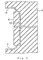
- Fig. 2 is a an enlarged sectional view showing a boundary portion between the insulated casing 5 and the insulating layer 4 of a modified molded electric device according to the embodiment.
- the same symbols are used for the same elements shown in Fig. 1, and detailed descriptions are omitted for those elements.
- a silane coupling agent layer 12 is formed between the insulating layer 4 and the unglazed outer surface of the insulated casing 5.
- Silane coupling agent layer 12 is formed by putting (coating) a silane coupling agent on the unglazed outer surface of insulated casing 5 before molding the insulated casing 5.
- the silane coupling agent includes an organic substance and silicon. More precisely, in one embodiment, silane coupling agent layer 12 is formed as below.
- vacuum circuit breaker 3 having insulated casing 5, which is made of ceramics, is prepared.
- the outer surface of insulated casing 5 is remained as naked (unglazed) surface.
- the naked outer surface of insulated casing 5 may be obtained, for example, by removing glaze by means of sandblasting.
- the liquid silane coupling agent is coated on the unglazed surface, for example, by using a brush so as not to cause coating irregularity.
- the liquid silane coupling agent may be diluted with a treatment agent.
- the treatment agent may be obtained by mixing water and alcohol.
- the liquid silane coupling diluent which is a liquid silane coupling agent diluted by the treatment agent, may lower the viscosity.
- the wettability is improved, and coating operation may be easily performed.
- the adhesiveness with the epoxy resin may be improved when using the liquid silane coupling diluent.
- Vacuum circuit breaker 3 coated with the silane coupling agent is set in a metal mold for forming an insulating layer 4.
- the metal mold with vacuum circuit breaker 3 is heated to a predetermined temperature, and the epoxy resin is injected in the metal mold. After the epoxy resin is cured and become the insulating layer 4, the silane coupling agent layer 12 is formed at a boundary portion between insulated casing 5 and insulating layer 4.
- Silane finished particles such as powdered silicon, alumina (aluminum oxides), or glasses, may be mixed with the epoxy resin as filler and may be used with a material of the insulating layer 4 to improve toughness of insulating layer 4.
- the toughness of insulating layer 4 may be further improved by using inorganic particles, such as powdered silicon, having at least two kind of particle size mixed up with rubber particles having a core-shell structure, as filler of the epoxy resin.
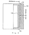
- Fig. 3 is a schematic half sectional diagram showing the experimental model that is used to investigate the dielectric strength at the boundary portion between the insulated casing and the insulating layer of the electric device according to the embodiment.
- the experimental model used in the investigation is an insulated casing 13 whose diameter ⁇ is 50 mm.
- a pair of ring-like electrodes 14 and 15 is disposed so as to surround insulated casing 13 with tip ends thereof separated by 10 mm.
- Electrodes 14 and 15 simulate the sealing metals 6 and 7 of the vacuum circuit breaker 3 shown in Figs. 1 and 2.
- the outer surface of insulated casing 13 is molded by an epoxy resin without glazing the outer surface of insulated casing 13. Circumferential side of electrodes 14 and 15 is also molded in the epoxy resin but each end of electrodes 14 and 15 is exposed.
- Epoxy resin is formed as insulating layer 16, which simulates the insulated layer 4 shown in Figs. 1 and 2.
- Example 1 Example 2, and comparative example.
- Examples 1 and 2 are based upon the embodiment discussed herein, which has insulated casing with an unglazed outer surface.
- Example 1 has no silane coupling agent layer in the boundary portion between insulated casing 13 and insulating layer 16, which simulates the configuration shown in Fig. 1.
- Example 2 has silane coupling agent layer in the boundary portion between insulated casing 13 and insulating layer 16, which simulates the configuration shown in Fig. 2.
- Comparative example has insulated casing 13 with glazed outer surface, which represents the conventional art. Comparative example has no silane coupling agent layer in the boundary portion between the insulated casing 13 and insulating layer 16.
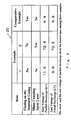
- Fig. 4 is a comparison chart of the investigations showing the lowest start and end voltage of partial discharge out of three investigations for each example.
- each row of a table 20 indicates the condition and result for each example mentioned above.
- Example 1 is improved by a substantial 1.4 times in the partial discharge characteristics of the start voltage of partial discharge and end voltage of partial discharge in comparison with that of Comparative example. Furthermore, Example 2 is improved by a substantial 9 times relative to Comparative example.
- Example 1 separations or cavities, which are considered as defects could not be confirmed at a boundary between ceramics of the insulated casing 13 and the insulating layer 16. Furthermore, in Example 2, the ceramics of the insulated casing 13 and the insulating layer 16 were strongly adhered through the silane coupling agent layer. In Comparative example, some cavities were found at a boundary between ceramics and the glaze.
- the molded electric device since a surface of the insulated casing 5 of the vacuum circuit breaker 3 is made of a naked (unglazed) ceramic surface, the partial discharge due to cavities in the glaze may not be formed, and thereby the dielectric strength can be improved.
- the silane coupling agent is coated on the naked ceramic surface so as to form the silane coupling agent layer between the insulated casing and the insulating layer, the adhesiveness with the insulating layer is improved, and thereby the dielectric strength may be further improved.
- a conductive paint such as silver paint, is coated on a surface of each of the sealing metals as the endplates, the adhesiveness between the insulating layer and each of the sealing metals can be improved, resulting in further improving the partial discharge characteristics and dielectric strength.
- the present invention is not restricted to an above embodiment.
- the molded electric device was explained with a vacuum circuit breaker; however, the invention can be applied also to an electric device in which an electric component such as a thyristor element or a zinc oxide element is accommodated in a ceramic cylindrical insulated casing.
- the endplate may not be a plate, but having a structure that can hold the electric component inside the insulated casing. Those structure may be easily obtained by one of ordinary skill in the art.
Landscapes
- Chemical & Material Sciences (AREA)
- Inorganic Chemistry (AREA)
- Engineering & Computer Science (AREA)
- Ceramic Engineering (AREA)
- High-Tension Arc-Extinguishing Switches Without Spraying Means (AREA)
- Gas-Insulated Switchgears (AREA)
- Casting Or Compression Moulding Of Plastics Or The Like (AREA)
- Insulating Bodies (AREA)
- Insulators (AREA)
- Moulds For Moulding Plastics Or The Like (AREA)
Applications Claiming Priority (2)
| Application Number | Priority Date | Filing Date | Title |
|---|---|---|---|
| JP2003202128 | 2003-07-25 | ||
| JP2003202128A JP4159938B2 (ja) | 2003-07-25 | 2003-07-25 | モールド電気機器およびそのモールド方法 |
Publications (3)
| Publication Number | Publication Date |
|---|---|
| EP1501101A2 true EP1501101A2 (fr) | 2005-01-26 |
| EP1501101A3 EP1501101A3 (fr) | 2005-12-28 |
| EP1501101B1 EP1501101B1 (fr) | 2008-04-23 |
Family
ID=33487671
Family Applications (1)
| Application Number | Title | Priority Date | Filing Date |
|---|---|---|---|
| EP04017233A Expired - Lifetime EP1501101B1 (fr) | 2003-07-25 | 2004-07-21 | Dispositif électrique moulé et méthode de moulage |
Country Status (6)
| Country | Link |
|---|---|
| US (1) | US20050029001A1 (fr) |
| EP (1) | EP1501101B1 (fr) |
| JP (1) | JP4159938B2 (fr) |
| KR (1) | KR100656233B1 (fr) |
| CN (1) | CN1577682A (fr) |
| DE (1) | DE602004013233T2 (fr) |
Cited By (3)
| Publication number | Priority date | Publication date | Assignee | Title |
|---|---|---|---|---|
| EP1983537A3 (fr) * | 2007-04-18 | 2009-11-25 | LS Industrial Systems Co., Ltd | Interrupteur d'aspirateur |
| EP2407991A1 (fr) * | 2010-07-12 | 2012-01-18 | Kabushiki Kaisha Toshiba | Soupape sous vide |
| EP3098828A4 (fr) * | 2014-01-24 | 2017-08-23 | Kabushiki Kaisha Toshiba, Inc. | Vanne de dépression et son processus de fabrication |
Families Citing this family (10)
| Publication number | Priority date | Publication date | Assignee | Title |
|---|---|---|---|---|
| JP5238349B2 (ja) * | 2008-05-19 | 2013-07-17 | 株式会社東芝 | 真空バルブ |
| CN101866765B (zh) * | 2009-04-20 | 2014-02-26 | 施耐德电器工业公司 | 一种用于中压断路器的主回路装配方法 |
| JP5367544B2 (ja) * | 2009-11-24 | 2013-12-11 | 株式会社東芝 | モールド真空バルブの試験方法 |
| US20120282473A1 (en) * | 2009-12-04 | 2012-11-08 | Owain Williams | Surface treatments and coatings |
| JP2016528362A (ja) * | 2013-08-22 | 2016-09-15 | ダウ グローバル テクノロジーズ エルエルシー | 回路遮断器極部分を製造するための方法 |
| DE102014210587A1 (de) * | 2014-06-04 | 2015-12-17 | Siemens Aktiengesellschaft | Verfahren zur Herstellung eines feststoffisolierten Schalterpols und feststoffisolierter Schalterpol |
| WO2016194464A1 (fr) * | 2015-06-05 | 2016-12-08 | 三菱電機株式会社 | Disjoncteur sous vide |
| DE102015213738A1 (de) * | 2015-07-21 | 2017-01-26 | Siemens Aktiengesellschaft | Energietechnische Komponente, insbesondere Vakuumschaltröhre |
| FR3070533B1 (fr) * | 2017-08-28 | 2019-09-13 | Schneider Electric Industries Sas | Pole de coupure de courant |
| JP7455648B2 (ja) * | 2020-04-20 | 2024-03-26 | 株式会社東芝 | モールド真空バルブの製造方法 |
Family Cites Families (12)
| Publication number | Priority date | Publication date | Assignee | Title |
|---|---|---|---|---|
| US3812314A (en) * | 1971-08-23 | 1974-05-21 | Gen Electric | High power electrical bushing having a vacuum switch encapsulated therein |
| CH596658A5 (fr) * | 1975-11-12 | 1978-03-15 | Sprecher & Schuh Ag | |
| JPH04345721A (ja) * | 1991-05-22 | 1992-12-01 | Meidensha Corp | 真空インタラプタ |
| JPH05282975A (ja) * | 1992-03-31 | 1993-10-29 | Toshiba Corp | モールド真空バルブ |
| JPH05298974A (ja) * | 1992-04-21 | 1993-11-12 | Toshiba Corp | 樹脂モールド真空バルブ |
| WO1994025973A1 (fr) * | 1993-04-29 | 1994-11-10 | Lindsey Manufacturing Company | Systeme electrique integre |
| JPH08306281A (ja) * | 1995-03-08 | 1996-11-22 | Fuji Electric Co Ltd | 真空遮断器用真空バルブ |
| MY119298A (en) * | 1996-09-13 | 2005-04-30 | Cooper Ind Inc | Encapsulated vacuum interrupter and method of making same |
| US5982253A (en) * | 1997-08-27 | 1999-11-09 | Nartron Corporation | In-line module for attenuating electrical noise with male and female blade terminals |
| JP3845534B2 (ja) * | 1999-12-01 | 2006-11-15 | 株式会社東芝 | スイッチギヤ |
| JP2003115244A (ja) | 2001-10-02 | 2003-04-18 | Toshiba Corp | モールド真空バルブ及びその接続方法 |
| US20040242034A1 (en) * | 2003-05-30 | 2004-12-02 | Hubbell Incorporated | Electrical assembly and dielectric material |
-
2003
- 2003-07-25 JP JP2003202128A patent/JP4159938B2/ja not_active Expired - Lifetime
-
2004
- 2004-07-21 DE DE602004013233T patent/DE602004013233T2/de not_active Expired - Lifetime
- 2004-07-21 EP EP04017233A patent/EP1501101B1/fr not_active Expired - Lifetime
- 2004-07-22 US US10/895,992 patent/US20050029001A1/en not_active Abandoned
- 2004-07-23 KR KR1020040057490A patent/KR100656233B1/ko not_active Expired - Fee Related
- 2004-07-23 CN CNA2004100684835A patent/CN1577682A/zh active Pending
Cited By (4)
| Publication number | Priority date | Publication date | Assignee | Title |
|---|---|---|---|---|
| EP1983537A3 (fr) * | 2007-04-18 | 2009-11-25 | LS Industrial Systems Co., Ltd | Interrupteur d'aspirateur |
| EP2407991A1 (fr) * | 2010-07-12 | 2012-01-18 | Kabushiki Kaisha Toshiba | Soupape sous vide |
| EP3098828A4 (fr) * | 2014-01-24 | 2017-08-23 | Kabushiki Kaisha Toshiba, Inc. | Vanne de dépression et son processus de fabrication |
| US9972467B2 (en) | 2014-01-24 | 2018-05-15 | Kabushiki Kaisha Toshiba | Vacuum valve and manufacturing method for the same |
Also Published As
| Publication number | Publication date |
|---|---|
| KR20050012672A (ko) | 2005-02-02 |
| EP1501101B1 (fr) | 2008-04-23 |
| DE602004013233T2 (de) | 2009-07-09 |
| JP4159938B2 (ja) | 2008-10-01 |
| US20050029001A1 (en) | 2005-02-10 |
| DE602004013233D1 (de) | 2008-06-05 |
| JP2005041063A (ja) | 2005-02-17 |
| CN1577682A (zh) | 2005-02-09 |
| KR100656233B1 (ko) | 2006-12-13 |
| EP1501101A3 (fr) | 2005-12-28 |
Similar Documents
| Publication | Publication Date | Title |
|---|---|---|
| EP1501101B1 (fr) | Dispositif électrique moulé et méthode de moulage | |
| RU2479061C2 (ru) | Изоляция коммутационного устройства типа вакуумного картриджа посредством формования заливкой | |
| JP4677005B2 (ja) | 真空インタラプタ | |
| EP0339791A1 (fr) | Isolateur eléctrique avec une fibre optique le transversant et procédé de fabrication de cet isolateur | |
| US6828521B2 (en) | Method for increasing insulation level in an encapsulation | |
| KR20020084807A (ko) | 점화 플러그의 제조방법 | |
| US4063991A (en) | Method of increasing voltage withstanding capability of vacuum interrupters | |
| CN104584344A (zh) | Esd保护器件及其制造方法 | |
| CN110936533B (zh) | 一种电极一体成型式聚合物基导电复合材料的制造方法 | |
| CN102479627A (zh) | 多功能新型模制电力设备及其制造方法 | |
| JPH06231661A (ja) | 樹脂モールド真空バルブ及びその製造方法 | |
| KR20220152603A (ko) | 전기화학 분석을 위한 일체형 몰드 전극 | |
| CN101461293A (zh) | 电路载体 | |
| JP2596275B2 (ja) | 電力用ケーブル接続部の組立方法 | |
| CN1320562C (zh) | 模制电器的接地层形成方法和外表面接地模制电器 | |
| JP2571483B2 (ja) | エポキシ樹脂絶縁成形体に導電性層を形成する方法 | |
| US11915895B2 (en) | Interrupter unit having a vacuum tube and an insulating housing | |
| CN102568716B (zh) | 绝缘支撑装置及其制造方法 | |
| JP3963589B2 (ja) | 電力ケーブル接続部の製造方法 | |
| JP3285693B2 (ja) | 注型成形品の製造方法 | |
| CN119805021A (zh) | 用于表面电位测量的装置及其加工装置和方法 | |
| JP2005271256A (ja) | 樹脂モールド品およびその製造方法 | |
| CN121079766A (zh) | 静电吸盘 | |
| DE19749395A1 (de) | Hochtemperaturstabile Anschlußkontaktverstärkung sowie Verfahren zu deren Herstellung | |
| JP2002290037A (ja) | 回路基板の製造方法 |
Legal Events
| Date | Code | Title | Description |
|---|---|---|---|
| PUAI | Public reference made under article 153(3) epc to a published international application that has entered the european phase |
Free format text: ORIGINAL CODE: 0009012 |
|
| 17P | Request for examination filed |
Effective date: 20040721 |
|
| AK | Designated contracting states |
Kind code of ref document: A2 Designated state(s): AT BE BG CH CY CZ DE DK EE ES FI FR GB GR HU IE IT LI LU MC NL PL PT RO SE SI SK TR |
|
| AX | Request for extension of the european patent |
Extension state: AL HR LT LV MK |
|
| PUAL | Search report despatched |
Free format text: ORIGINAL CODE: 0009013 |
|
| AK | Designated contracting states |
Kind code of ref document: A3 Designated state(s): AT BE BG CH CY CZ DE DK EE ES FI FR GB GR HU IE IT LI LU MC NL PL PT RO SE SI SK TR |
|
| AX | Request for extension of the european patent |
Extension state: AL HR LT LV MK |
|
| RIC1 | Information provided on ipc code assigned before grant |
Ipc: 7H 01B 3/02 A Ipc: 7H 01B 3/12 B |
|
| AKX | Designation fees paid |
Designated state(s): DE FR |
|
| 17Q | First examination report despatched |
Effective date: 20070206 |
|
| GRAP | Despatch of communication of intention to grant a patent |
Free format text: ORIGINAL CODE: EPIDOSNIGR1 |
|
| GRAS | Grant fee paid |
Free format text: ORIGINAL CODE: EPIDOSNIGR3 |
|
| GRAA | (expected) grant |
Free format text: ORIGINAL CODE: 0009210 |
|
| AK | Designated contracting states |
Kind code of ref document: B1 Designated state(s): DE FR |
|
| REF | Corresponds to: |
Ref document number: 602004013233 Country of ref document: DE Date of ref document: 20080605 Kind code of ref document: P |
|
| ET | Fr: translation filed | ||
| PLBE | No opposition filed within time limit |
Free format text: ORIGINAL CODE: 0009261 |
|
| STAA | Information on the status of an ep patent application or granted ep patent |
Free format text: STATUS: NO OPPOSITION FILED WITHIN TIME LIMIT |
|
| 26N | No opposition filed |
Effective date: 20090126 |
|
| REG | Reference to a national code |
Ref country code: FR Ref legal event code: PLFP Year of fee payment: 13 |
|
| REG | Reference to a national code |
Ref country code: FR Ref legal event code: PLFP Year of fee payment: 14 |
|
| REG | Reference to a national code |
Ref country code: FR Ref legal event code: PLFP Year of fee payment: 15 |
|
| PGFP | Annual fee paid to national office [announced via postgrant information from national office to epo] |
Ref country code: FR Payment date: 20220609 Year of fee payment: 19 |
|
| PGFP | Annual fee paid to national office [announced via postgrant information from national office to epo] |
Ref country code: DE Payment date: 20220524 Year of fee payment: 19 |
|
| REG | Reference to a national code |
Ref country code: DE Ref legal event code: R119 Ref document number: 602004013233 Country of ref document: DE |
|
| PG25 | Lapsed in a contracting state [announced via postgrant information from national office to epo] |
Ref country code: DE Free format text: LAPSE BECAUSE OF NON-PAYMENT OF DUE FEES Effective date: 20240201 |
|
| PG25 | Lapsed in a contracting state [announced via postgrant information from national office to epo] |
Ref country code: FR Free format text: LAPSE BECAUSE OF NON-PAYMENT OF DUE FEES Effective date: 20230731 |