EP1496519A2 - Procédé de codage et dispositif de mémoire - Google Patents
Procédé de codage et dispositif de mémoire Download PDFInfo
- Publication number
- EP1496519A2 EP1496519A2 EP04023697A EP04023697A EP1496519A2 EP 1496519 A2 EP1496519 A2 EP 1496519A2 EP 04023697 A EP04023697 A EP 04023697A EP 04023697 A EP04023697 A EP 04023697A EP 1496519 A2 EP1496519 A2 EP 1496519A2
- Authority
- EP
- European Patent Office
- Prior art keywords
- data
- bit
- bit data
- code
- encoder
- Prior art date
- Legal status (The legal status is an assumption and is not a legal conclusion. Google has not performed a legal analysis and makes no representation as to the accuracy of the status listed.)
- Granted
Links
Images


Classifications
-
- G—PHYSICS
- G11—INFORMATION STORAGE
- G11C—STATIC STORES
- G11C16/00—Erasable programmable read-only memories
-
- G—PHYSICS
- G06—COMPUTING; CALCULATING OR COUNTING
- G06F—ELECTRIC DIGITAL DATA PROCESSING
- G06F11/00—Error detection; Error correction; Monitoring
- G06F11/07—Responding to the occurrence of a fault, e.g. fault tolerance
- G06F11/08—Error detection or correction by redundancy in data representation, e.g. by using checking codes
- G06F11/10—Adding special bits or symbols to the coded information, e.g. parity check, casting out 9's or 11's
- G06F11/1008—Adding special bits or symbols to the coded information, e.g. parity check, casting out 9's or 11's in individual solid state devices
- G06F11/1068—Adding special bits or symbols to the coded information, e.g. parity check, casting out 9's or 11's in individual solid state devices in sector programmable memories, e.g. flash disk
-
- G—PHYSICS
- G06—COMPUTING; CALCULATING OR COUNTING
- G06F—ELECTRIC DIGITAL DATA PROCESSING
- G06F11/00—Error detection; Error correction; Monitoring
- G06F11/07—Responding to the occurrence of a fault, e.g. fault tolerance
- G06F11/08—Error detection or correction by redundancy in data representation, e.g. by using checking codes
- G06F11/10—Adding special bits or symbols to the coded information, e.g. parity check, casting out 9's or 11's
- G06F11/1008—Adding special bits or symbols to the coded information, e.g. parity check, casting out 9's or 11's in individual solid state devices
- G06F11/1072—Adding special bits or symbols to the coded information, e.g. parity check, casting out 9's or 11's in individual solid state devices in multilevel memories
-
- G—PHYSICS
- G11—INFORMATION STORAGE
- G11C—STATIC STORES
- G11C11/00—Digital stores characterised by the use of particular electric or magnetic storage elements; Storage elements therefor
- G11C11/56—Digital stores characterised by the use of particular electric or magnetic storage elements; Storage elements therefor using storage elements with more than two stable states represented by steps, e.g. of voltage, current, phase, frequency
- G11C11/5621—Digital stores characterised by the use of particular electric or magnetic storage elements; Storage elements therefor using storage elements with more than two stable states represented by steps, e.g. of voltage, current, phase, frequency using charge storage in a floating gate
-
- G—PHYSICS
- G11—INFORMATION STORAGE
- G11C—STATIC STORES
- G11C29/00—Checking stores for correct operation ; Subsequent repair; Testing stores during standby or offline operation
-
- G—PHYSICS
- G11—INFORMATION STORAGE
- G11C—STATIC STORES
- G11C29/00—Checking stores for correct operation ; Subsequent repair; Testing stores during standby or offline operation
- G11C29/04—Detection or location of defective memory elements, e.g. cell constructio details, timing of test signals
- G11C29/08—Functional testing, e.g. testing during refresh, power-on self testing [POST] or distributed testing
- G11C29/12—Built-in arrangements for testing, e.g. built-in self testing [BIST] or interconnection details
- G11C29/38—Response verification devices
- G11C29/42—Response verification devices using error correcting codes [ECC] or parity check
-
- G—PHYSICS
- G11—INFORMATION STORAGE
- G11C—STATIC STORES
- G11C7/00—Arrangements for writing information into, or reading information out from, a digital store
- G11C7/10—Input/output [I/O] data interface arrangements, e.g. I/O data control circuits, I/O data buffers
- G11C7/1006—Data managing, e.g. manipulating data before writing or reading out, data bus switches or control circuits therefor
-
- H—ELECTRICITY
- H03—ELECTRONIC CIRCUITRY
- H03M—CODING; DECODING; CODE CONVERSION IN GENERAL
- H03M13/00—Coding, decoding or code conversion, for error detection or error correction; Coding theory basic assumptions; Coding bounds; Error probability evaluation methods; Channel models; Simulation or testing of codes
- H03M13/03—Error detection or forward error correction by redundancy in data representation, i.e. code words containing more digits than the source words
- H03M13/05—Error detection or forward error correction by redundancy in data representation, i.e. code words containing more digits than the source words using block codes, i.e. a predetermined number of check bits joined to a predetermined number of information bits
- H03M13/13—Linear codes
- H03M13/15—Cyclic codes, i.e. cyclic shifts of codewords produce other codewords, e.g. codes defined by a generator polynomial, Bose-Chaudhuri-Hocquenghem [BCH] codes
-
- G—PHYSICS
- G11—INFORMATION STORAGE
- G11C—STATIC STORES
- G11C16/00—Erasable programmable read-only memories
- G11C16/02—Erasable programmable read-only memories electrically programmable
- G11C16/04—Erasable programmable read-only memories electrically programmable using variable threshold transistors, e.g. FAMOS
Definitions
- the present invention relates to an encoding method and a memory apparatus applicable preferably to a multi-valued recording flash memory, a memory card using that flash memory and so on.
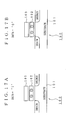
- Figs. 17A and 17B illustrate a structure of a memory cell 100 used in a flash memory. That is, the memory cell 100 is so formed as to stack a charge storage layer (floating gate) 102 and a control gate 103 on a semiconductor substrate 101.
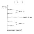
- the quantity of charge held in the floating gate 102 is controlled so that it is reached to one of two threshold voltages shown in Fig. 18 according to the data ("0" or "1") to be recorded.
- the data item is to be read from the memory cell 100, by using a reference voltage set between the two threshold voltages, it is determined that the data item in the memory cell 100 is judged to be "0" or "1" depending on whether the threshold voltage of the memory cell 100 is higher or lower than the reference voltage.
- an error correcting circuit based on an error correcting code such as the Hamming code is often incorporated in the semiconductor memory in order to counter aging-induced failures such as faulty cells, resulting in particular from an increasing number of write and erase operations.
- the error correcting code is a redundant code called check data attached to information data and then the check data are used to correct an error in the entire code.
- check data For example, 10-bit check data as shown in Fig. 19 are added to an abbreviated Hamming code for a 512-bit block of information data so that, even if one error occurs in the 522-bit code, the error may be corrected.
- Fig. 20 shows a structure of a flash memory 110 incorporating an error correcting circuit based on the Hamming code therein.
- the flash memory 110 comprises cell arrays 111 having a plurality of memory cells, an encoder 112 converting input data Din into an abbreviated Hamming code to provide write data WD to be written to the cell arrays 111 and a Hamming code decoder 113 providing output data Dout by subjecting read data RD retrieved from the cell arrays 111 to an error correction process.
- the encoder 112 and Hamming code decoder 113 constitute an error correcting circuit.
- the encoder 112 adds 10-bit check data to every 512-bit block of input data Din and the abbreviated Hamming code for the 512-bit information data is created.
- a data write operation takes place as follows. That is, input data Din are first inputted to the encoder 112. Then, the encoder 112 converts the input data Din into the abbreviated Hamming code for 512-bit information data, thereby generating write data WD. The write data WD outputted from the encoder 112 are fed and written to the cell arrays 111.
- a data read operation is carried out as follows.
- Read data RD retrieved from the cell arrays 111 are inputted to the Hamming code decoder 113. If one code of the read data RD contains no error, the Hamming code decoder 113 outputs the information data unchanged as output data Dout. If one code of the read data RD has one erroneous bit, the Hamming code decoder 113 outputs the information data as the output data Dout after correcting the error.
- an abbreviated BCH code Bose-Chaudhuri-Hocquenghem code
- Bose-Chaudhuri-Hocquenghem code Bose-Chaudhuri-Hocquenghem code
- the BCH code and techniques of code abbreviation are discussed illustratively by Hideki Imai in "Code Grafs" (Institute of Electronics, Information and Communication Engineers of Japan) among others.
- 20-bit check data are added to the abbreviated BCH code for 512-bit information data as shown in Fig. 21, thereby enabling to correct two errors in the 532-bit code.
- Fig. 22 shows a structure of a flash memory 120 incorporating an error correcting circuit based on the BCH code.
- the flash memory 120 comprises cell arrays 121 having a plurality of memory cells, an encoder 122 for converting input data Din into an abbreviated BCH code to provide write data WD to be written to the cell arrays 121 and a BCH code decoder 123 for subjecting read data RD retrieved from the cell arrays 121 to an error correction process to provide output data Dout.
- the encoder 122 and the BCH code decoder 123 constitute an error correcting circuit.
- the encoder 122 adds 20-bit check data to every 512-bit block of input data Din and the abbreviated BCH code capable of correcting two errors regarding the 512-bit information data is created.
- a data write operation takes place as follows. That is, input data Din are first inputted to the encoder 122. Then, the encoder 122 converts the input data Din into the abbreviated BCH code for 512-bit information data, thereby generating write data WD. The write data WD outputted from the encoder 122 are fed and written to the cell arrays 121.
- a data read operation is carried out as follows.
- Read data RD retrieved from the cell arrays 121 is inputted to the BCH code decoder 123. If one code of the read data RD contains no error, the BCH code decoder 123 outputs the information data unchanged as output data Dout. If one code of the read data RD has one or two erroneous bits, the information data are outputted as the output data Dout after correcting the error.
- the error correcting circuit incorporated in the flash memory 110 or 120 can suppress errors of written data despite a certain number of faulty cells caused by aging.
- a relatively large quantity of the check data, which are redundant check data are required to correct a fairly large number of errors and thus, the number of memory cells to be used is increased as well as the scale of the error correcting circuit to be incorporated is enlarged.
- the memory card constituted by a plurality of flash memories (flash memory chips) will be described.
- the memory card includes multiple flash memories and a controller.
- Fig. 23 shows a structure of a memory card 130 with a controller having an error correcting circuit based on the BCH code.
- the memory card 130 includes two flash memories 131 and 132 and a controller 133 for writing and reading data to and from these flash memories 131 and 132.
- the controller 133 comprises a card interface 134 for exchanging data with an entity outside the card, an encoder 135 for converting input data Din into an abbreviated BCH code to provide write data WD to be written to the flash memories 131 and 132, a BCH code decoder 136 for subjecting read data RD from the flash memories 131 and 132 to an error correction process to provide output data Dout, and a flash interface 137 for controlling the writing and reading of data to and from the flash memories 131 and 132.
- the encoder 135 and the BCH code decoder 136 constitute an error correcting circuit.
- the encoder 135 adds 20-bit check data to every 512-bit block of input data Din, thus creating an abbreviated BCH code capable of correcting two errors regarding the 512-bit information data.
- a data write operation takes place as follows. That is, input data Din are first taken into the card by the card interface 134 and supplied to the encoder 135. Then, the encoder 135 converts the input data Din into the abbreviated BCH code for 512-bit information data, thereby generating write data WD. The write data WD outputted from the encoder 135 are written to the flash memory 131 or 132 under control of the flash interface 137.
- a data read operation is carried out as follows.
- Read data RD retrieved from the flash memory 131 or 132 under control of the flash interface 137 are inputted to the BCH code decoder 136. If one code of the read data RD contains no error, the BCH code decoder 136 outputs the information data unchanged as output data Dout. If one code of the read data RD has one or two erroneous bits, the BCH code decoder 136 outputs the information data as the output data Dout after correcting the error(s). In this way, the output data Dout are outputted from the BCH code decoder 136 to an entity outside the card via the card interface 134.
- the error correcting code is also used in a memory card made of a plurality of flash memories. If a controller is used for error correction, it is possible to have a characteristic that error correcting circuit larger than an error correcting circuit incorporated in the flash memory is obtained so that the greater number of errors may be corrected.
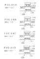
- Figs. 24A through 24D the quantity of charge accumulated in a floating gate 102 in a memory cell 100 of a flash memory for four-value recording is controlled so that it may attain one of four threshold voltages shown in Fig. 25 representing a data item to be stored ("11,” “10,” “01” or "00").
- threshold voltages shown in Fig. 25 representing a data item to be stored ("11,” “10,” “01” or "00").
- three reference voltages each established between the respective adjacent threshold values are used.
- the threshold value in the memory cell 100 By comparing the threshold value in the memory cell 100 with each of the reference voltages, the data from the memory cell 100 are retrieved. This arrangement allows each memory cell 100 to store two-bit information.
- Multi-value recording flash memories may, as with their binary recording counterparts, utilize an error correcting circuit as well.
- Fig. 26 shows a structure of a flash memory 140 for 16-value (4-bit) recording incorporating an error correcting circuit based on the BCH code.
- the flash memory 140 comprises cell arrays 141 having a plurality of memory cells, an encoder 142 for converting input data Din into an abbreviated BCH code to provide write data WD to be written to the cell arrays 141 and a one-bit/four-bit converter 143 for converting write data WD outputted from the encoder 142 from serial data format to four-bit parallel data format and supplying the converted data to the cell arrays 141.
- the flash memory 140 also includes a four-bit/one-bit converter 144 for converting read data RD retrieved from the cell arrays 141 from four-bit parallel data format to serial data format and a BCH code decoder 145 for providing output data Dout by subjecting to an error correction process the read data RD converted to serial data by the four-bit/one-bit converter 144.
- the encoder 142 and the BCH code decoder 145 constitute an error correcting circuit.
- the encoder 142 adds 20-bit check data to every 512-bit block of input data Din, thereby creating an abbreviated BCH code capable of correcting two errors regarding the 512-bit information data.
- a data write operation takes place as follows. That is, input data Din are first inputted to the encoder 142. Then, the encoder 142 converts the input data Din into the abbreviated BCH code for 512-bit information data, thereby generating write data WD.
- the write data WD outputted from the encoder 142 are converted by the one-bit/four-bit converter 143 from serial data format to four-bit parallel data format (four-bit data for storage into memory cells) , thus supplying the write data WD to the cell arrays 141 and writing the data WD consecutively to each of memory cells making up the cell arrays 141.
- a data read operation is carried out as follows.
- Read data RD retrieved from cell arrays 141 are converted by the four-bit/one-bit converter 144 from four-bit parallel data format to serial data format.
- the converted serial data are supplied to the BCH code decoder 145. If one code of the read data RD contains no error, the BCH code decoder 145 outputs the information data unchanged as output data Dout. If one code of the read data RD has one or two erroneous bits, the BCH code decoder 145 outputs the information data as the output data Dout after correcting the error(s).
- the multi-value recording flash memories such as the flash memory 140 shown in Fig. 26 have such a characteristic that a single faulty cell causes multiple erroneous bits. Since conventional flash memories have stored one bit per memory cell, these memories principally have used code systems for bit error correction as their error correcting code. However, if a single faulty memory cell results in a plurality of erroneous bits, the error correcting code for bit-by-bit error correction is inefficient.
- a memory apparatus comprising cell arrays having a plurality of memory cells each storing multi-bit information, an encoder for converting input data into a Reed-Solomon code to provide write data to be written to the cell arrays and a Reed-Solomon code decoder for subjecting read data retrieved from the cell arrays to an error correction process to provide output data.
- a memory apparatus comprising a memory portion having cell arrays made of a plurality of memory cells each storing multi-bit data and a controller for writing and reading data to and from the memory portion wherein the controller includes an encoder for converting input data into a Reed-Solomon code to provide write data to be written to the memory portion and a Reed-Solomon code decoder for subjecting read data retrieved from the memory portion to an error correction process to provide output data.
- each memory cell of the cell arrays stores multi-bit data.
- the encoder converts input data into a Reed-Solomon code as write data to be written to the cell arrays.
- the Reed-Solomon code reckons a plurality of bits as one byte and is an error correction code used for error correction in units of bytes.
- multi-bit data are read from each memory cell of the cell arrays and the read data are subjected to an error correction process by the Reed-Solomon code decoder, thereby providing output data.
- the Reed-Solomon code for error correction in units of bytes is thus used as the error correcting code for the memory apparatus made of memory cells each storing multi-bit data so that it is possible to provide sufficient performance involving a limited number of correcting errors.
- This makes it possible to reduce the error correcting circuit in scale with a smaller number of memory cells to be used than before.
- an encoding method comprising the steps of supplementing (n-m) bit data with m-bit data for conversion into n-bit data, n being greater than m, encoding the n-bit data using a Reed-Solomon code reckoning n bits as one symbol, and outputting as information data the m-bit data before supplementing the (n-m) bit data while outputting as check data the m-bit data after having undergone n-bit/m-bit conversion.
- a memory apparatus comprising cell arrays having a plurality of memory cells, an encoder for converting input data into an error correcting code to provide write data to be written to the cell arrays, and a decoder for subjecting read data retrieved from the cell arrays to an error correction process to provide output data, characterized in that the encoder supplements (n-m) bit data with m-bit input data for conversion into n-bit data, n being greater than m, encodes the n-bit data using a Reed-Solomon code reckoning n bits as one symbol and outputs as information data the m-bit data before supplementing the (n-m) bit data while outputting as check data the m-bit data after having undergone n-bit/m-bit conversion and that the decoder supplements the (n-m) bit data relating to an information data part thereof with the m-bit read data retrieved from the cell arrays for conversion into n-bit data, subjects a check data part to
- a memory apparatus comprising a memory portion having cell arrays made of a plurality of memory cells and a controller for writing and reading data to and from the memory portion, characterized in that the controller includes an encoder for converting input data into an error correcting code to provide write data to be written to the memory portion, and a decoder for subjecting read data retrieved from the memory portion to an error correction process to provide output data, wherein the encoder supplements (n-m) bit data with m-bit input data for conversion into n-bit data, n being greater than m, encodes the n-bit data using a Reed-Solomon code reckoning n bits as one symbol and outputs as information data the m-bit data before supplementing the (n-m) bit data while outputting as check data the m-bit data after having undergone n-bit/m-bit conversion, and wherein the decoder supplements the n-m bit data with m-bit read data retrieved from the cell array
- each memory cell of the cell arrays stores data of one bit or plural bits.
- m-bit input data are inputted to the encoder.
- the (n-m) bit data (n > m) of, for example, 0 are supplemented with m-bit input data for conversion into n-bit data.
- eight-bit input data are supplemented with two-bit zeros for conversion into 10-bit data.
- the n-bit data are then converted to a Reed-Solomon code reckoning n bites as one symbol.
- the m-bit data before supplementing the (n-m) bit data are outputted as information data, while the m-bit data after having undergone n-bit/m-bit conversion are outputted as check data. Then, the m-bit data outputted from the encoder are fed and written successively to cells of the cell arrays.
- the Reed-Solomon code is an error correcting code that reckons a plurality of bits as one symbol for error correction in units of symbols.
- the m-bit data retrieved from the cell arrays are inputted to the decoder.
- the (n-m) bit data are supplemented with the m-bit data for an information data part thereof for conversion into n-bit data, and a check data part thereof is subjected to m-bit/n-bit conversion into n-bit data, whereby the Reed-Solomon code reckoning n bits as one symbol is reconstituted.
- the reconstituted Reed-Solomon code is subjected to an error correction process.
- an m-bit part of the corrected n-bit information data is outputted as the output data.
- the input and the output data are both m-bit data whereas the encoder uses for its encoding operation the Reed-Solomon code reckoning n bits (n > m) as one symbol. Therefore, this makes it possible to extend the code length while maintaining data exchanges with an external entity in units of m bits. For this reason, there is no need to divide information data of a predetermined length into segments for encoding purposes. This makes it possible to reduce check data (redundant data) while preserving the continuity of decoded data.
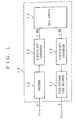
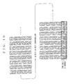
- Fig. 1 shows a structure of a flash memory 10 practiced as the first embodiment of the invention.
- the flash memory 10 designed for 16-value (4-bit) recording incorporates an error correcting circuit based on the abbreviated Reed-Solomon code capable of double-error correction.
- Each of the Reed-Solomon code and the abbreviated Reed-Solomon code reckons a plurality of bits as one byte to correct error in a unit of byte. Details of the Reed-Solomon code are described illustratively in the above-cited publication "Code Grafs" by Hideki Imai (Institute of Electronics, Information and Communication Engineers of Japan) among others.
- the flash memory 10 comprises cell arrays 11 having a plurality of memory cells, an encoder 12 for converting eight-bit parallel input data Din into an abbreviated Reed-Solomon code to provide write data WD to be written to the cell arrays 11 and an eight-bit/four-bit converter 13 for converting one-byte (8-bit) parallel write data WD outputted by the encoder 12 into four-bit parallel data (four-bit data to be stored in memory cell) that are fed to the cell arrays 11, as shown in Fig. 3.
- the flash memory 10 further includes a four-bit/eight-bit converter 14 for converting four-bit parallel read data RD retrieved from the cell arrays 11 into one-byte (8-bit) parallel data as shown in Fig. 3, and a Reed-Solomon code decoder 15 for subjecting read data RD converted as one-byte parallel data in the four-bit/eight-bit converter 14 to an error correction process to provide output data Dout.
- the encoder 12 and the Reed-Solomon code decoder 15 constitute an error correcting circuit. Then, the encoder 12 supplements each 128-byte block of input data Din with four-byte check data to generate an abbreviated Reed-Solomon code for correcting two errors in the 128-byte block of information data.
- a data write operation is carried out as follows. That is, eight-bit parallel input data Din are inputted to the encoder 12. Then, the encoder 12 converts the input data Din into an abbreviated Reed-Solomon code for 128 bytes of information data to provide write data WD. The one-byte (8-bit) parallel write data WD outputted by the encoder 12 are converted by the eight-bit/four-bit converter 13 into four-bit parallel data to be fed to the cell arrays 11 so that the converted data are written consecutively to memory cells making up the cell arrays 11.
- a data read operation takes place as follows.
- Four-bit parallel read data RD retrieved from the cell arrays 11 are converted by the four-bit/eight-bit converter 14 into one-byte (8-bit) parallel data that are supplied to the Reed-Solomon code decoder 15. If one code of read data RD has no error, the Reed-Solomon code decoder 15 outputs information data unchanged as output data Dout in units of bytes. If one code of the read data RD has one or two erroneous bytes, the Reed-Solomon code decoder 15 outputs information data as the output data Dout in units of bytes after correcting the error (s).
- a bit converter may be furnished upstream of the encoder 12 to convert the input data Din into eight-bit parallel data, or a bit converter may be installed downstream of the Reed-Solomon code decoder 15 to convert the eight-bit parallel data into parallel or serial data representing the output data Dout.
- the Reed-Solomon code is employed as an error correcting code for correcting errors in units of bytes in the cell arrays 11 made of memory cells each storing four-bit data and then sufficient performance may be attained with a limited number of correcting errors. Therefore, this makes it possible to reduce the error correcting circuit in scale and make smaller a number of memory cells to be used.
- the abbreviated BCH code is used for the correction of up to eight erroneous bits in 128 bytes, that is, 1,024-bit information data, 88 bits of check data are needed. Since one defective cell requires the correction of four bits, this error correcting code for eight-error correction permits correction of up to two faulty cells. Since 1,112 bits are stored in 278 cells and one block contains 256 codes, the probability of a block getting faulty is about 0.000091% as calculated by the expression (1) below.
- the probability of a block becoming faulty is then acquired when the abbreviated Reed-Solomon code for double-error correction is used. In this case, errors of up to two bytes can be corrected.
- the byte error rate is defined by the expression (2) below with eight bits of two-cell information regarded as one byte.
- the probability of a block getting defective is estimated at about 0.000077%.
- the abbreviated BCH code for eight-error correction and the abbreviated Reed-Solomon code for two-error correction have approximately the same error correcting capability.
- two errors for correction by the Reed-Solomon code are much smaller opposed to eight errors for correction by the BCH code
- use of Reed-Solomon code allows a scale of error correcting circuit to be composed as a far smaller one than that of BHC code.
- 32 bits of redundant data for the Reed-Solomon code are much smaller with compared with 88 bits of redundant data for the BCH code, a far smaller number of memory cells can be used therefor.
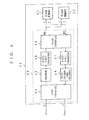
- Fig. 4 depicts a structure of a memory card 20 practiced as the second embodiment of the invention.
- the memory card 20 comprises two flash memories for 16-value (4-bit) recording and a controller incorporating an error correcting circuit based on the abbreviated Reed-Solomon code for double-error correction.
- the memory card 20 includes two flash memories 21 and 22 as well as a controller 23 for writing and reading data to and from the flash memories 21 and 22.
- the controller 23 has a card interface 24 for exchanging data with an entity outside the card, an encoder 25 for converting eight-bit parallel input data Din into an abbreviated Reed-Solomon code to provide write data WD to be written to the flash memories 21 and 22, and an eight-bit/four-bit converter 26 for converting the write data WD of one-byte (8-bit) parallel data outputted by the encoder 25 into four-bit parallel data (four-bit data to be stored in memory cells) as depicted in Fig. 3.
- the controller 23 further comprises a four-bit/eight-bit converter 27 for converting four-bit parallel read data RD retrieved from the flash memory 21 or 22 into one-byte (8-bit) parallel data as shown in Fig. 3, a Reed-Solomon code decoder 28 for subjecting to an error correction process the one-byte parallel read data RD converted in the four-bit/eight-bit converter 27 to provide output data Dout, and a flash interface 29 for controlling the writing and reading of data to and from the flash memories 21 and 22.
- a four-bit/eight-bit converter 27 for converting four-bit parallel read data RD retrieved from the flash memory 21 or 22 into one-byte (8-bit) parallel data as shown in Fig. 3
- a Reed-Solomon code decoder 28 for subjecting to an error correction process the one-byte parallel read data RD converted in the four-bit/eight-bit converter 27 to provide output data Dout
- a flash interface 29 for controlling the writing and reading of data to and from the flash memories 21 and 22
- the encoder 25 and the Reed-Solomon code decoder 28 constitute an error correcting circuit. Then, the encoder 25 supplements each 128-byte block of input data Din with four-byte check data to generate an abbreviated Reed-Solomon code for correcting two errors in the 128-byte information data.
- a data write operation is carried out as follows. That is, input data Din is taken into the card through the card interface 24 and sent to the encoder 25.
- the encoder 25 converts the input data Din into an abbreviated Reed-Solomon code for 128 bytes of information data to provide write data WD.
- the eight-bit/four-bit converter 26 converts the one-byte (8-bit) parallel write data WD outputted by the encoder 25 into four-bit parallel data.
- the converted four-bit parallel data are written to the flash memory 21 or the flash memory 22 under control of the flash interface 29.
- a data read operation takes place as follows.
- Four-bit parallel read data RD retrieved from the flash memory 21 or the flash memory 22 under control of the flash interface 29 are converted by the four-bit/eight-bit converter 27 into one-byte (8-bit) parallel data.
- the converted one-byte parallel data are fed to the Reed-Solomon code decoder 28. If one code of read data RD has no error, the Reed-Solomon code decoder 28 outputs information data unchanged as output data Dout in units of bytes. If one code of the read data RD has one or two erroneous bytes, the Reed-Solomon code decoder 28 outputs information data as the output data Dout in units of bytes after correcting the error(s). In this way, the output data Dout outputted by the Reed-Solomon code decoder 28 are sent out of the card through the card interface 24.
- a bit converter may be furnished upstream of the encoder 25 to convert the input data Din into eight-bit parallel data, or a bit converter may be installed downstream of the Reed-Solomon code decoder 28 to convert the eight-bit parallel data into parallel or serial data representing the output data Dout.
- the Reed-Solomon code is employed as the error correcting code for error correction in units of bytes in the flash memories 21 and 22, which constitute a memory portion, made of cell arrays comprising memory cells each storing four-bit data.
- the second embodiment provides sufficient performance involving a limited number of errors to be corrected. Accordingly, the second embodiment also makes it possible to reduce the error correcting circuit in scale with a smaller number of memory cells incorporated. Further, since the controller 23 corrects errors, the error correcting circuit is allowed to be larger in scale than if the error correcting circuit is incorporated in the flash memory 21 or 22. Therefore, even if a large number of errors result from multi-value recording, they can be corrected.
- Fig. 6 shows a state of coding wherein 512-byte data are encoded illustratively by four abbreviated Reed-Solomon codes each capable of correcting one error in 128 bytes of information data.
- decoded data of one page are outputted with intervening blanks when decoded (see Fig. 7). From a system performance point of view, decoded data of one page should be outputted uninterrupted as much as possible. Therefore, in that respect, it is also preferable for data of one page to be encoded as one block.
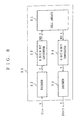
- Fig. 8 shows a structure of a flash memory 30 practiced as the third embodiment of the invention.
- the flash memory 30 permits data exchanges with an outside entity in units of bytes (8 bits).
- This flash memory 30 for 16-value (4-bit) recording incorporates an error correcting circuit based on the abbreviated Reed-Solomon code capable of double-error correction.
- the check data (redundant data) for double-error correction comprise four symbols requiring a 516-byte code length. Since the Reed-Solomon code reckoning 10 bits as one symbol is 1,023 bytes long, the 516-byte-long code is made available through abbreviation. Further, the check data comprising four symbols amounts to 40 bits representing five bytes.
- the flash memory 30 includes cell arrays 31 having a plurality of memory cells, an encoder 32 for converting eight-bit parallel input data Din into an abbreviated Reed-Solomon code to provide write data WD to be written to the cell arrays 31, and an eight-bit/four-bit converter 33 for converting eight-bit write data WD outputted by the encoder 32 into four-bit data (four-bit data to be stored in memory cells) that are supplied to the cell arrays 31, as shown in Fig. 3.
- the flash memory 30 comprises a four-bit/eight-bit converter 34 for converting four-bit read data RD retrieved from the cell arrays 31 into eight-bit data as shown in Fig. 3, and a decoder 35 for subjecting to an error correction process the eight-bit read data RD converted in the four-bit/eight-bit converter 34 to provide output data Dout.
- the encoder 32 and the decoder 35 constitute an error correcting circuit.
- Fig. 9 shows a structure of the encoder 32.
- the encoder 32 includes an eight-bit/10-bit converter 32a for converting eight-bit data as input data Din into 10-bit data by supplementing them with two-bit zeros as shown in Fig. 10, and a Reed-Solomon encoder 32b for encoding 10-bit data outputted by the converter 32a by use of the Reed-Solomon code reckoning 10 bits as one symbol.
- the Reed-Solomon encoder 32b supplements each 512-symbol block of 10-bit data with four-symbol check data (redundant data) to generate an abbreviated Reed-Solomon code capable of correcting two errors in 512 symbols.
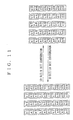
- the encoder 32 comprises a 10-bit/eight-bit converter 32c for removing two bits from 10-bit data for conversion into eight-bit data, a 10-bit/eight-bit converter 32d for changing the bit configuration of 10-bit data for conversion into eight-bit data as shown in Fig.
- a changeover switch 32e for selectively supplying to the converters 32c and 32d the 512-symbol information data and four-symbol check data constituting each Reed-Solomon code outputted by the Reed-Solomon encoder 32b, and a changeover switch 32f for selectively outputting as write data WD the eight-bit data corresponding to the 512-symbol information data from the converter 32c and the eight-bit data corresponding to the four-symbol check data from the converter 32d.
- the converter 32c When supplied with the 512-symbol information data, the converter 32c outputs 512-byte data making up an information data part.
- the converter 32d outputs five-byte data forming a check data part.
- Eight-bit input data Din of eight-bit data are fed to the eight-bit/10-bit converter 32a wherein the eight-bit data are supplemented with two-bit zeros for conversion into 10-bit data.
- the 10-bit data are supplied to the Reed-Solomon encoder 32b and converted into an abbreviated Reed-Solomon code for correcting two errors in the 512-symbol information data.
- the 512-symbol information data are sent to the 10-bit/eight-bit converter 32c, through the changeover switch 32e, wherein the two-bit zeros added by above-described eight-bit/10-bit converter 32a are removed from the supplied 10-bit data for conversion into eight-bit data (see Fig. 10). Then, the resulting eight-bit data are outputted as write data WD via the changeover switch 32f.
- each 516-symbol Reed-Solomon code outputted from the Reed-Solomon encoder 32b the four-symbol check data are fed to the 10-bit/eight-bit converter 32d, through the changeover switch 32e, wherein the bit configuration of the check data is changed for conversion into eight-bit data (see Fig. 11). Then, the converted eight-bit data are outputted as write data WD via the changeover switch 32f.
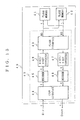
- Fig. 12 shows a structure of the decoder 35.
- the decoder 35 comprises an eight-bit/10-bit converter 35a for supplementing eight-bit data with two-bit zeros for conversion into 10-bit data as shown in Fig. 10, an eight-bit/10-bit converter 35b for changing the bit configuration of eight-bit data for conversion into 10-bit data as shown in Fig. 11, a changeover switch 35c for selectively supplying each 512-byte information data part and each five-byte check data part of eight-bit read data RD outputted from the four-bit/eight-bit converter 34 (in Fig.
- the decoder 35 includes a Reed-Solomon code decoder 35e for subjecting to an error correction process the Reed-Solomon code outputted by the changeover switch 35d, and a 10-bit/eight-bit converter 35f for removing two bits from the 10-bit information data having undergone error correction by the decoder 35e, for conversion into eight-bit data to provide output data Dout, as shown in Fig. 13.
- each 512-byte information data part is supplied to the eight-bit/10-bit converter 35a wherein two-bit zeros are added to the supplied data for conversion into 10-bit data (see Fig. 10).
- each five-byte check data part is supplied to the eight-bit/10-bit converter 35b wherein the bit configuration of the supplied data is changed for conversion into 10-bit data (see Fig. 11).
- the changeover switch 35d selectively extracts the 10-bit data corresponding to the 512-byte information data part outputted by the converter 35a and the 10-bit data corresponding to the five-byte check data part outputted by the converter 35b, so that the abbreviated Reed-Solomon code for correcting two errors in the 512-symbol information data may be reconstituted.
- the Reed-Solomon code outputted by the changeover switch 35d is supplied to the Reed-Solomon code decoder 35e. If one code contains one or two erroneous symbols, the Reed-Solomon code decoder 35e corrects the error(s). After the error correction by the decoder 35e, the 10-bit data as information data are supplied to the 10-bit/eight-bit converter 35f wherein two bits are removed from the supplied data for conversion into eight-bit data (see Fig. 13) to provide output data Dout.
- a data write operation is carried out as follows. That is, one-byte (8-bit) input data Din are fed to the encoder 32. Then, the encoder 32 adds two-byte zeros to the input data Din for conversion into 10-bit data. The 10-bit data are converted to a Reed-Solomon code capable of correcting two errors in 512-symbol information data. The eight-bit data before supplementing with 0 are outputted as information data, while the eight-bit data after the change of the bit configuration are outputted as check data. Then, the eight-bit write data WD outputted by the encoder 32 are converted by the eight-bit/four-bit converter 33 into four-bit data and fed to the cell arrays 31. The supplied four-bit data are written successively to memory cells making up the cell arrays 31.
- a data read operation takes place as follows.
- Four-bit read data RD retrieved from the cell arrays 31 are converted by the four-bit/eight-bit converter 34 into eight-bit data that are fed to the decoder 35.
- the decoder 35 adds two-bit zeros to each 512-byte information data part for conversion into 10-bit data; each five-byte check data part has its bit configuration changed for conversion from eight-bit to 10-bit data. This reconstitutes the Reed-Solomon code capable of correcting two errors in the 512-symbol information data.
- the decoder 35 subjects the reconstituted Reed-Solomon code to an error correction process. From the corrected information data, two bits are removed for conversion into eight-bit data that are outputted as the output data Dout in units of bytes.
- the input data Din and the output data Dout are eight-bit data and the encoder 32 performs its encoding operation using the Reed-Solomon code reckoning 10 bits as one symbol and thus, this makes it possible to extend the code length while maintaining data exchanges with an external entity in units of one byte (8 bits). Accordingly, there is no need to divide, for example, 512-byte information data making up each page into segments for encoding purposes.
- the scheme makes it possible to reduce check data (redundant data) while preserving the continuity of each page of 512-byte decoded data as shown in Fig. 14.
- the abbreviated Reed-Solomon code is used for double-error correction in a 512-byte information data part, with five-byte check data (redundant data) added to the data part as in the third embodiment, the probability of a faulty block becoming a reality is obtained.
- one abbreviated Reed-Solomon code can correct up to two symbols. If eight-bit information corresponding to two cells is regarded as one symbol, the rate of a symbol getting erroneous is given by the expression (4) below. The symbol error rate thus furnished is that of information data.
- the symbol error rate of check data (redundant data) is about 2.5 times the rate of a cell getting faulty, i.e., 2.5 x 10 -5 . 1-(1-1.0 ⁇ 10 -5 ) 2 ⁇ 2.0 ⁇ 10 -5
- the total number of symbols is 516, and one block contains 64 codes. Because the symbol error rate of check data is higher than that of information data, the probability of a block becoming defective is evaluated through the use of the symbol error rate regarding check data. Accordingly, the probability of a faulty block becoming a reality is evaluated from the expression (5) and estimated approximately at 0.0023% or less.
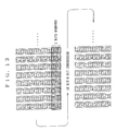
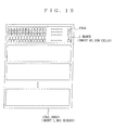
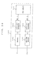
- FIG. 15 shows a structure of a memory card 40 practiced as the fourth embodiment of the invention.
- This memory card 40 uses two flash memories for 16-value (4-bit) recording, and has a controller incorporating an error correcting circuit based on the abbreviated Reed-Solomon code reckoning 10 bits as one symbol for double-error correction.
- the memory card 40 comprises two flash memories 41 and 42 as well as a controller 43 for writing and reading data to and from these flash memories 41 and 42.
- the controller 43 comprises a card interface 44 for exchanging data with an entity outside the card, an encoder 45 for converting eight-bit parallel input data Din into an abbreviated Reed-Solomon code to provide write data WD to be written to the flash memories 41 and 42, and an eight-bit/four-bit converter 46 for converting eight-bit write data WD outputted by the encoder 45 into four-bit data (four-bit data to be stored in memory cells) as shown in Fig. 3.
- the encoder 45 has the same structure as the encoder 32 (see Fig. 9) of the flash memory 30 in Fig. 8, so that a detailed description of the encoder 45 is omitted.
- the controller 43 comprises a four-bit/eight-bit converter 47 for converting four-bit read data RD retrieved from the flash memory 41 or 42 into eight-bit data as shown in Fig. 3, a decoder 48 for subjecting to an error correction process the eight-bit read data RD converted in the four-bit/eight-bit converter 47 to provide output data Dout, and a flash interface 49 for controlling the writing and reading of data to and from the flash memories 41 and 42.
- the decoder 48 has the same structure as the decoder 35 (see Fig. 12) of the flash memory 30 in Fig. 8, so that a detailed description of the decoder 48 is omitted.
- a data write operation in the memory card 40 of Fig. 15 is carried out as follows. That is, input data Din are taken into the card through the card interface 44 and fed to the encoder 45. Then, the encoder 45 supplements the input data Din with two-bit zeros for conversion into 10-bit data which in turn are converted into a Reed-Solomon code for correcting two errors in 512-symbol information data, and thus, the eight-bit data before supplementing with 0 are outputted as information data, while the eight-bit data after the change of the bit configuration are outputted as check data. Then, the eight-bit write data WD outputted by the encoder 45 are converted by the eight-bit/four-bit converter 46 into four-bit data that are written to the flash memory 41 or 42 under control of the flash interface 49.
- a data read operation takes place as follows.
- Four-bit read data RD retrieved from the flash memory 41 or 42 under control of the flash interface 49 are converted by the four-bit/eight-bit converter 47 into eight-bit data that are fed to the decoder 48.
- the decoder 48 supplements each 512-byte information data part with two-bit zeros to convert the eight-bit data into 10-bit data, and each five-byte check data part has its bit configuration changed for conversion from eight-bit to 10-bit data so that the Reed-Solomon code capable of correcting two errors in the 512-symbol information data is reconstituted.
- the decoder 48 subjects the reconstituted Reed-Solomon code to an error correction process and two bits are removed from the corrected information data for conversion into eight-bit data that are outputted as the output data Dout in units of bytes. In this way, the output data Dout outputted by the decoder 48 are sent out of the card through the card interface 44.
- the input data Din and the output data Dout are also eight-bit data and the encoder 45 performs its encoding operation using the Reed-Solomon code reckoning 10 bits as one symbol, so that it is possible to extend the code length while maintaining data exchanges with an external entity in units of one byte (8 bits). Accordingly, there is no need to divide, for example, 512-byte information data making up each page into segments for encoding purposes and then it possible to reduce check data (redundant data) while preserving the continuity of each page of 512-byte decoded data as shown in Fig. 14.
- the conversion into 10-bit data may be accomplished by use of other two-bit data. In such cases, the same two-bit data should be added to each information data part for conversion into 10-bit data at the time of decoding.
- a number of cell regarded as one byte is not limited to these two-cell data, so that other alterations such that one-cell data are regarded as one byte or three or other appropriate number of cells of data are regarded as one byte, may be conceived.
- first through the fourth embodiments above have been shown adopting a flash memory arrangement as their storage system, but the invention is not limited to flash memories but may be applied alternatively to other diverse storage systems such as semiconductor memories.
- the Reed-Solomon code for error correction in units of bytes is used as the error correcting code applied to a memory arrangement composed of memory cells each storing multi-bit data, thereby providing sufficient performance involving a limited number of correcting errors, reducing the error correcting circuit in scale with a smaller number of memory cells incorporated than before.
- the input and output data are m-bit data and the encoder performs its encoding operation using the Reed-Solomon code reckoning n bits (n > m) as one symbol, it possible to extend the code length while maintaining data exchanges with an external entity in units of m bits. Therefore, there is no need to divide each information data part of a predetermined length into segments for encoding purposes, thereby reducing the amount of check data (redundant data) while preserving the continuity of decoded data.
- the encoding method and memory apparatus according to the invention may be adapted advantageously to multi-value recording flash memories and memory cards using such memories, among others.
Applications Claiming Priority (5)
| Application Number | Priority Date | Filing Date | Title |
|---|---|---|---|
| JP995898 | 1998-01-21 | ||
| JP00995798A JP4099844B2 (ja) | 1998-01-21 | 1998-01-21 | メモリ装置 |
| JP995898A JPH11212876A (ja) | 1998-01-21 | 1998-01-21 | 符号化方法およびそれを利用したメモリ装置 |
| JP995798 | 1998-01-21 | ||
| EP99901130A EP0969480A4 (fr) | 1998-01-21 | 1999-01-21 | Procede de codage et dispositif de memoire |
Related Parent Applications (1)
| Application Number | Title | Priority Date | Filing Date |
|---|---|---|---|
| EP99901130A Division EP0969480A4 (fr) | 1998-01-21 | 1999-01-21 | Procede de codage et dispositif de memoire |
Publications (3)
| Publication Number | Publication Date |
|---|---|
| EP1496519A2 true EP1496519A2 (fr) | 2005-01-12 |
| EP1496519A3 EP1496519A3 (fr) | 2005-02-09 |
| EP1496519B1 EP1496519B1 (fr) | 2006-08-23 |
Family
ID=26344787
Family Applications (2)
| Application Number | Title | Priority Date | Filing Date |
|---|---|---|---|
| EP04023697A Expired - Lifetime EP1496519B1 (fr) | 1998-01-21 | 1999-01-21 | Procédé de codage et dispositif de mémoire |
| EP99901130A Ceased EP0969480A4 (fr) | 1998-01-21 | 1999-01-21 | Procede de codage et dispositif de memoire |
Family Applications After (1)
| Application Number | Title | Priority Date | Filing Date |
|---|---|---|---|
| EP99901130A Ceased EP0969480A4 (fr) | 1998-01-21 | 1999-01-21 | Procede de codage et dispositif de memoire |
Country Status (6)
| Country | Link |
|---|---|
| US (1) | US6732322B1 (fr) |
| EP (2) | EP1496519B1 (fr) |
| KR (1) | KR100535291B1 (fr) |
| CN (1) | CN1256005A (fr) |
| DE (1) | DE69932962T2 (fr) |
| WO (1) | WO1999038170A1 (fr) |
Cited By (1)
| Publication number | Priority date | Publication date | Assignee | Title |
|---|---|---|---|---|
| WO2008082591A2 (fr) * | 2007-01-02 | 2008-07-10 | Marvell World Trade Ltd. | Interface haute vitesse pour une mémoire à multiples niveaux |
Families Citing this family (50)
| Publication number | Priority date | Publication date | Assignee | Title |
|---|---|---|---|---|
| JP4074029B2 (ja) * | 1999-06-28 | 2008-04-09 | 株式会社東芝 | フラッシュメモリ |
| JP4417629B2 (ja) * | 2001-04-24 | 2010-02-17 | エヌエックスピー ビー ヴィ | ビット変更を可能にする、フラッシュメモリにおける使用のための、改良されたエラー修正方式 |
| KR100893428B1 (ko) * | 2001-07-25 | 2009-04-17 | 소니 가부시끼 가이샤 | 인터페이스 장치 |
| US6981196B2 (en) * | 2001-07-25 | 2005-12-27 | Hewlett-Packard Development Company, L.P. | Data storage method for use in a magnetoresistive solid-state storage device |
| JP4112849B2 (ja) * | 2001-11-21 | 2008-07-02 | 株式会社東芝 | 半導体記憶装置 |
| US6904492B2 (en) * | 2001-12-19 | 2005-06-07 | Hewlett-Packard Development Company, L.P. | Write-once memory device including non-volatile memory for temporary storage |
| JP2006004560A (ja) * | 2004-06-18 | 2006-01-05 | Elpida Memory Inc | 半導体記憶装置及びその誤り訂正方法 |
| GB2428496A (en) * | 2005-07-15 | 2007-01-31 | Global Silicon Ltd | Error correction for flash memory |
| US7681109B2 (en) * | 2005-10-13 | 2010-03-16 | Ramot At Tel Aviv University Ltd. | Method of error correction in MBC flash memory |
| ATE468558T1 (de) * | 2006-03-07 | 2010-06-15 | Nxp Bv | Elektronische schaltung mit einer speichermatrix zur speicherung von seiten einschliesslich zusätzlicher daten |
| CN101192924B (zh) * | 2006-11-24 | 2011-01-26 | 北京大学 | 基于Reed-Solomon码的P2P存储系统编码方法 |
| KR100845529B1 (ko) | 2007-01-03 | 2008-07-10 | 삼성전자주식회사 | 플래시 메모리 장치의 이씨씨 제어기 및 그것을 포함한메모리 시스템 |
| CN101067972B (zh) * | 2007-04-23 | 2012-04-25 | 北京兆易创新科技有限公司 | 一种存储器检错纠错编码电路及利用其读写数据的方法 |
| US8065583B2 (en) * | 2007-07-06 | 2011-11-22 | Micron Technology, Inc. | Data storage with an outer block code and a stream-based inner code |
| US8051358B2 (en) | 2007-07-06 | 2011-11-01 | Micron Technology, Inc. | Error recovery storage along a nand-flash string |
| JP5127350B2 (ja) * | 2007-07-31 | 2013-01-23 | 株式会社東芝 | 半導体記憶装置 |
| US8046542B2 (en) * | 2007-11-21 | 2011-10-25 | Micron Technology, Inc. | Fault-tolerant non-volatile integrated circuit memory |
| US8499229B2 (en) * | 2007-11-21 | 2013-07-30 | Micro Technology, Inc. | Method and apparatus for reading data from flash memory |
| US7826277B2 (en) * | 2008-03-10 | 2010-11-02 | Hynix Semiconductor Inc. | Non-volatile memory device and method of operating the same |
| KR101466695B1 (ko) * | 2008-04-30 | 2014-12-01 | 삼성전자주식회사 | 멀티 비트 레벨 데이터의 부호화 및 복호화 방법 |
| WO2009136357A1 (fr) * | 2008-05-09 | 2009-11-12 | Koninklijke Philips Electronics N.V. | Système de motivation pour faire ses devoirs |
| GB2492708B (en) * | 2010-03-30 | 2017-01-25 | Ibm | Data encoding in solid state storage devices |
| US8386895B2 (en) | 2010-05-19 | 2013-02-26 | Micron Technology, Inc. | Enhanced multilevel memory |
| US8972821B2 (en) * | 2010-12-23 | 2015-03-03 | Texas Instruments Incorporated | Encode and multiplex, register, and decode and error correction circuitry |
| KR101736337B1 (ko) | 2011-02-28 | 2017-05-30 | 삼성전자주식회사 | 비휘발성 메모리 장치, 상기 메모리 장치를 제어하는 컨트롤러, 및 상기 컨트롤러 동작 방법 |
| US8782494B2 (en) * | 2011-10-04 | 2014-07-15 | Cleversafe, Inc. | Reproducing data utilizing a zero information gain function |
| KR101813182B1 (ko) * | 2011-11-16 | 2017-12-29 | 삼성전자주식회사 | 비휘발성 메모리 소자를 포함하는 다치 논리 장치 |
| DE112012005424T5 (de) | 2011-12-21 | 2014-09-18 | International Business Machines Corporation | Lese/Schreib-Operationen in Halbleiterspeicher-Bauelementen |
| US9740484B2 (en) | 2011-12-22 | 2017-08-22 | Intel Corporation | Processor-based apparatus and method for processing bit streams using bit-oriented instructions through byte-oriented storage |
| US9176812B1 (en) | 2012-05-22 | 2015-11-03 | Pmc-Sierra, Inc. | Systems and methods for storing data in page stripes of a flash drive |
| US9021333B1 (en) | 2012-05-22 | 2015-04-28 | Pmc-Sierra, Inc. | Systems and methods for recovering data from failed portions of a flash drive |
| US8972824B1 (en) | 2012-05-22 | 2015-03-03 | Pmc-Sierra, Inc. | Systems and methods for transparently varying error correction code strength in a flash drive |
| US8996957B1 (en) | 2012-05-22 | 2015-03-31 | Pmc-Sierra, Inc. | Systems and methods for initializing regions of a flash drive having diverse error correction coding (ECC) schemes |
| US9047214B1 (en) | 2012-05-22 | 2015-06-02 | Pmc-Sierra, Inc. | System and method for tolerating a failed page in a flash device |
| US9021336B1 (en) | 2012-05-22 | 2015-04-28 | Pmc-Sierra, Inc. | Systems and methods for redundantly storing error correction codes in a flash drive with secondary parity information spread out across each page of a group of pages |
| US8793556B1 (en) | 2012-05-22 | 2014-07-29 | Pmc-Sierra, Inc. | Systems and methods for reclaiming flash blocks of a flash drive |
| US8788910B1 (en) | 2012-05-22 | 2014-07-22 | Pmc-Sierra, Inc. | Systems and methods for low latency, high reliability error correction in a flash drive |
| US9183085B1 (en) | 2012-05-22 | 2015-11-10 | Pmc-Sierra, Inc. | Systems and methods for adaptively selecting from among a plurality of error correction coding schemes in a flash drive for robustness and low latency |
| US9021337B1 (en) | 2012-05-22 | 2015-04-28 | Pmc-Sierra, Inc. | Systems and methods for adaptively selecting among different error correction coding schemes in a flash drive |
| US9577673B2 (en) | 2012-11-08 | 2017-02-21 | Micron Technology, Inc. | Error correction methods and apparatuses using first and second decoders |
| US9081701B1 (en) | 2013-03-15 | 2015-07-14 | Pmc-Sierra, Inc. | Systems and methods for decoding data for solid-state memory |
| US9009565B1 (en) | 2013-03-15 | 2015-04-14 | Pmc-Sierra, Inc. | Systems and methods for mapping for solid-state memory |
| US9026867B1 (en) | 2013-03-15 | 2015-05-05 | Pmc-Sierra, Inc. | Systems and methods for adapting to changing characteristics of multi-level cells in solid-state memory |
| US9208018B1 (en) | 2013-03-15 | 2015-12-08 | Pmc-Sierra, Inc. | Systems and methods for reclaiming memory for solid-state memory |
| US9053012B1 (en) | 2013-03-15 | 2015-06-09 | Pmc-Sierra, Inc. | Systems and methods for storing data for solid-state memory |
| KR102299880B1 (ko) * | 2017-04-04 | 2021-09-09 | 에스케이하이닉스 주식회사 | 데이터 변환 장치 및 방법 |
| TWI643201B (zh) | 2017-11-27 | 2018-12-01 | 慧榮科技股份有限公司 | 編碼器及相關的編碼方法與快閃記憶體控制器 |
| TWI665678B (zh) * | 2017-11-27 | 2019-07-11 | 慧榮科技股份有限公司 | 編碼器及相關的編碼方法與快閃記憶體控制器 |
| CN110147873B (zh) * | 2018-05-18 | 2020-02-18 | 中科寒武纪科技股份有限公司 | 卷积神经网络的处理器及训练方法 |
| KR20210129960A (ko) * | 2020-04-21 | 2021-10-29 | 삼성전자주식회사 | 채널들에 신호들을 송신하는 송신기, 채널들로부터 신호들을 수신하는 수신기, 및 이들을 포함하는 반도체 시스템 |
Citations (4)
| Publication number | Priority date | Publication date | Assignee | Title |
|---|---|---|---|---|
| JPS6167322A (ja) * | 1984-09-11 | 1986-04-07 | Nec Home Electronics Ltd | リ−ドソロモン符号・復号方式の訂正用メモリ制御回路 |
| US5233610A (en) * | 1989-08-30 | 1993-08-03 | Mitsubishi Denki Kabushiki Kaisha | Semiconductor memory device having error correcting function |
| US5394362A (en) * | 1991-02-08 | 1995-02-28 | Banks; Gerald J. | Electrically alterable non-voltatile memory with N-bits per memory cell |
| US5450363A (en) * | 1994-06-02 | 1995-09-12 | Intel Corporation | Gray coding for a multilevel cell memory system |
Family Cites Families (12)
| Publication number | Priority date | Publication date | Assignee | Title |
|---|---|---|---|---|
| US5226043A (en) * | 1990-12-27 | 1993-07-06 | Raytheon Company | Apparatus and method for data error detection and correction and address error detection in a memory system |
| US5459742A (en) * | 1992-06-11 | 1995-10-17 | Quantum Corporation | Solid state disk memory using storage devices with defects |
| JPH06195896A (ja) * | 1992-12-28 | 1994-07-15 | Canon Inc | 記録再生装置、記録装置及び再生装置 |
| KR950001695A (ko) * | 1993-06-18 | 1995-01-03 | 오오가 노리오 | 디스크 재생장치 |
| US5475716A (en) * | 1994-01-18 | 1995-12-12 | Gi Corporation | Method for communicating block coded digital data with associated synchronization/control data |
| JP3560074B2 (ja) * | 1994-07-29 | 2004-09-02 | ソニー株式会社 | 記録再生装置、及びメモリ制御装置 |
| JP3153730B2 (ja) * | 1995-05-16 | 2001-04-09 | 株式会社東芝 | 不揮発性半導体記憶装置 |
| US5719884A (en) * | 1995-07-27 | 1998-02-17 | Hewlett-Packard Company | Error correction method and apparatus based on two-dimensional code array with reduced redundancy |
| JPH09134313A (ja) * | 1995-11-10 | 1997-05-20 | Sony Corp | メモリ装置 |
| JP3275697B2 (ja) | 1996-04-05 | 2002-04-15 | 株式会社日立製作所 | 記録再生装置 |
| JPH09288895A (ja) * | 1996-04-19 | 1997-11-04 | Toshiba Corp | 3値記憶半導体記憶システム |
| US5864569A (en) * | 1996-10-18 | 1999-01-26 | Micron Technology, Inc. | Method and apparatus for performing error correction on data read from a multistate memory |
-
1999
- 1999-01-21 WO PCT/JP1999/000217 patent/WO1999038170A1/fr active IP Right Grant
- 1999-01-21 CN CN99800053A patent/CN1256005A/zh active Pending
- 1999-01-21 EP EP04023697A patent/EP1496519B1/fr not_active Expired - Lifetime
- 1999-01-21 EP EP99901130A patent/EP0969480A4/fr not_active Ceased
- 1999-01-21 KR KR10-1999-7008621A patent/KR100535291B1/ko not_active IP Right Cessation
- 1999-01-21 DE DE69932962T patent/DE69932962T2/de not_active Expired - Lifetime
- 1999-01-21 US US09/381,661 patent/US6732322B1/en not_active Expired - Lifetime
Patent Citations (4)
| Publication number | Priority date | Publication date | Assignee | Title |
|---|---|---|---|---|
| JPS6167322A (ja) * | 1984-09-11 | 1986-04-07 | Nec Home Electronics Ltd | リ−ドソロモン符号・復号方式の訂正用メモリ制御回路 |
| US5233610A (en) * | 1989-08-30 | 1993-08-03 | Mitsubishi Denki Kabushiki Kaisha | Semiconductor memory device having error correcting function |
| US5394362A (en) * | 1991-02-08 | 1995-02-28 | Banks; Gerald J. | Electrically alterable non-voltatile memory with N-bits per memory cell |
| US5450363A (en) * | 1994-06-02 | 1995-09-12 | Intel Corporation | Gray coding for a multilevel cell memory system |
Non-Patent Citations (1)
| Title |
|---|
| PATENT ABSTRACTS OF JAPAN vol. 0102, no. 36 (E-428), 15 August 1986 (1986-08-15) & JP 61 067322 A (NEC HOME ELECTRONICS LTD), 7 April 1986 (1986-04-07) * |
Cited By (6)
| Publication number | Priority date | Publication date | Assignee | Title |
|---|---|---|---|---|
| WO2008082591A2 (fr) * | 2007-01-02 | 2008-07-10 | Marvell World Trade Ltd. | Interface haute vitesse pour une mémoire à multiples niveaux |
| WO2008082591A3 (fr) * | 2007-01-02 | 2008-12-04 | Marvell World Trade Ltd | Interface haute vitesse pour une mémoire à multiples niveaux |
| US7978541B2 (en) | 2007-01-02 | 2011-07-12 | Marvell World Trade Ltd. | High speed interface for multi-level memory |
| US8432753B2 (en) | 2007-01-02 | 2013-04-30 | Marvell World Trade Ltd. | High speed interface for multi-level memory |
| US8638619B2 (en) | 2007-01-02 | 2014-01-28 | Marvell World Trade Ltd. | High speed interface for multi-level memory |
| TWI453755B (zh) * | 2007-01-02 | 2014-09-21 | Marvell World Trade Ltd | 用於多層記憶體之高速介面 |
Also Published As
| Publication number | Publication date |
|---|---|
| EP1496519A3 (fr) | 2005-02-09 |
| DE69932962D1 (de) | 2006-10-05 |
| US6732322B1 (en) | 2004-05-04 |
| WO1999038170A1 (fr) | 1999-07-29 |
| KR20010005558A (ko) | 2001-01-15 |
| EP1496519B1 (fr) | 2006-08-23 |
| KR100535291B1 (ko) | 2005-12-09 |
| EP0969480A4 (fr) | 2000-11-22 |
| CN1256005A (zh) | 2000-06-07 |
| EP0969480A1 (fr) | 2000-01-05 |
| DE69932962T2 (de) | 2007-02-01 |
Similar Documents
| Publication | Publication Date | Title |
|---|---|---|
| EP1496519B1 (fr) | Procédé de codage et dispositif de mémoire | |
| KR100327883B1 (ko) | 인터리빙을 사용한 멀티레벨 셀 메모리의 정정 방법 및 장치 | |
| US8626988B2 (en) | System and method for uncoded bit error rate equalization via interleaving | |
| US6336203B1 (en) | Error correction coding and decoding method, and circuit using said method | |
| CN101183565B (zh) | 存储介质中数据校验方法 | |
| JP5232014B2 (ja) | 符号化及び信号処理機能を有するフラッシュメモリ | |
| US8122303B2 (en) | Data structure for flash memory and data reading/writing method thereof | |
| EP2218003B1 (fr) | Correction d'erreurs dans une matrice mémoire | |
| US20130305119A1 (en) | Method and Device for Correction of Ternary Stored Binary Data | |
| US8635508B2 (en) | Systems and methods for performing concatenated error correction | |
| JPH11283396A (ja) | メモリ装置 | |
| EP1282040A2 (fr) | Procédé de stockage de données dans un mémoire à semi-conducteurs magnétorésistif | |
| US20110296272A1 (en) | Outer code protection for solid state memory devices | |
| WO2011121490A1 (fr) | Codes bch à deux niveaux pour dispositifs de stockage à semi-conducteurs | |
| KR20080106849A (ko) | 재생 장치 | |
| EP2447842A1 (fr) | Procédé et système pour la correction des erreurs dans un réseau de mémoire | |
| CN101281788A (zh) | 闪存系统及其控制方法 | |
| US8463982B2 (en) | Method of storing and accessing error correcting code in NAND flash | |
| JPH11143787A (ja) | 記録再生装置 | |
| JP4099844B2 (ja) | メモリ装置 | |
| JPH11212876A (ja) | 符号化方法およびそれを利用したメモリ装置 | |
| JPH11213693A (ja) | メモリ装置 | |
| US9299460B1 (en) | Data structure of defective address information and defective address information encoding method for memory array | |
| KR101172672B1 (ko) | 부호길이 동기화가 적용된 메모리 장치 및 이의 부호길이 동기화 방법 |
Legal Events
| Date | Code | Title | Description |
|---|---|---|---|
| PUAI | Public reference made under article 153(3) epc to a published international application that has entered the european phase |
Free format text: ORIGINAL CODE: 0009012 |
|
| PUAL | Search report despatched |
Free format text: ORIGINAL CODE: 0009013 |
|
| AC | Divisional application: reference to earlier application |
Ref document number: 0969480 Country of ref document: EP Kind code of ref document: P |
|
| AK | Designated contracting states |
Kind code of ref document: A2 Designated state(s): DE FR GB |
|
| AK | Designated contracting states |
Kind code of ref document: A3 Designated state(s): DE FR GB |
|
| RIC1 | Information provided on ipc code assigned before grant |
Ipc: 7G 11C 29/00 A Ipc: 7G 11C 11/56 B |
|
| 17P | Request for examination filed |
Effective date: 20050427 |
|
| 17Q | First examination report despatched |
Effective date: 20050525 |
|
| AKX | Designation fees paid |
Designated state(s): DE FR GB |
|
| GRAP | Despatch of communication of intention to grant a patent |
Free format text: ORIGINAL CODE: EPIDOSNIGR1 |
|
| GRAS | Grant fee paid |
Free format text: ORIGINAL CODE: EPIDOSNIGR3 |
|
| GRAA | (expected) grant |
Free format text: ORIGINAL CODE: 0009210 |
|
| AC | Divisional application: reference to earlier application |
Ref document number: 0969480 Country of ref document: EP Kind code of ref document: P |
|
| AK | Designated contracting states |
Kind code of ref document: B1 Designated state(s): DE FR GB |
|
| REG | Reference to a national code |
Ref country code: GB Ref legal event code: FG4D |
|
| REF | Corresponds to: |
Ref document number: 69932962 Country of ref document: DE Date of ref document: 20061005 Kind code of ref document: P |
|
| ET | Fr: translation filed | ||
| PLBE | No opposition filed within time limit |
Free format text: ORIGINAL CODE: 0009261 |
|
| STAA | Information on the status of an ep patent application or granted ep patent |
Free format text: STATUS: NO OPPOSITION FILED WITHIN TIME LIMIT |
|
| 26N | No opposition filed |
Effective date: 20070524 |
|
| REG | Reference to a national code |
Ref country code: DE Ref legal event code: R084 Ref document number: 69932962 Country of ref document: DE |
|
| REG | Reference to a national code |
Ref country code: GB Ref legal event code: 746 Effective date: 20150424 |
|
| REG | Reference to a national code |
Ref country code: DE Ref legal event code: R084 Ref document number: 69932962 Country of ref document: DE Effective date: 20150410 |
|
| REG | Reference to a national code |
Ref country code: FR Ref legal event code: PLFP Year of fee payment: 18 |
|
| REG | Reference to a national code |
Ref country code: FR Ref legal event code: PLFP Year of fee payment: 19 |
|
| REG | Reference to a national code |
Ref country code: FR Ref legal event code: PLFP Year of fee payment: 20 |
|
| PGFP | Annual fee paid to national office [announced via postgrant information from national office to epo] |
Ref country code: GB Payment date: 20180119 Year of fee payment: 20 Ref country code: DE Payment date: 20180122 Year of fee payment: 20 |
|
| PGFP | Annual fee paid to national office [announced via postgrant information from national office to epo] |
Ref country code: FR Payment date: 20180119 Year of fee payment: 20 |
|
| REG | Reference to a national code |
Ref country code: DE Ref legal event code: R071 Ref document number: 69932962 Country of ref document: DE |
|
| REG | Reference to a national code |
Ref country code: GB Ref legal event code: PE20 Expiry date: 20190120 |
|
| PG25 | Lapsed in a contracting state [announced via postgrant information from national office to epo] |
Ref country code: GB Free format text: LAPSE BECAUSE OF EXPIRATION OF PROTECTION Effective date: 20190120 |