EP1496367B1 - Halter für einen leitfähigen kontakt - Google Patents
Halter für einen leitfähigen kontakt Download PDFInfo
- Publication number
- EP1496367B1 EP1496367B1 EP03723132.1A EP03723132A EP1496367B1 EP 1496367 B1 EP1496367 B1 EP 1496367B1 EP 03723132 A EP03723132 A EP 03723132A EP 1496367 B1 EP1496367 B1 EP 1496367B1
- Authority
- EP
- European Patent Office
- Prior art keywords
- holder
- base plate
- opening
- contact probe
- hole forming
- Prior art date
- Legal status (The legal status is an assumption and is not a legal conclusion. Google has not performed a legal analysis and makes no representation as to the accuracy of the status listed.)
- Expired - Lifetime
Links
Images


Classifications
-
- G—PHYSICS
- G01—MEASURING; TESTING
- G01R—MEASURING ELECTRIC VARIABLES; MEASURING MAGNETIC VARIABLES
- G01R1/00—Details of instruments or arrangements of the types included in groups G01R5/00 - G01R13/00 and G01R31/00
- G01R1/02—General constructional details
- G01R1/06—Measuring leads; Measuring probes
- G01R1/067—Measuring probes
- G01R1/06711—Probe needles; Cantilever beams; "Bump" contacts; Replaceable probe pins
- G01R1/06716—Elastic
- G01R1/06722—Spring-loaded
-
- G—PHYSICS
- G01—MEASURING; TESTING
- G01R—MEASURING ELECTRIC VARIABLES; MEASURING MAGNETIC VARIABLES
- G01R1/00—Details of instruments or arrangements of the types included in groups G01R5/00 - G01R13/00 and G01R31/00
- G01R1/02—General constructional details
- G01R1/06—Measuring leads; Measuring probes
- G01R1/067—Measuring probes
- G01R1/073—Multiple probes
- G01R1/07307—Multiple probes with individual probe elements, e.g. needles, cantilever beams or bump contacts, fixed in relation to each other, e.g. bed of nails fixture or probe card
- G01R1/07314—Multiple probes with individual probe elements, e.g. needles, cantilever beams or bump contacts, fixed in relation to each other, e.g. bed of nails fixture or probe card the body of the probe being perpendicular to test object, e.g. bed of nails or probe with bump contacts on a rigid support
-
- G—PHYSICS
- G01—MEASURING; TESTING
- G01R—MEASURING ELECTRIC VARIABLES; MEASURING MAGNETIC VARIABLES
- G01R1/00—Details of instruments or arrangements of the types included in groups G01R5/00 - G01R13/00 and G01R31/00
- G01R1/02—General constructional details
- G01R1/06—Measuring leads; Measuring probes
- G01R1/067—Measuring probes
- G01R1/06711—Probe needles; Cantilever beams; "Bump" contacts; Replaceable probe pins
Definitions
- the present invention relates to an electroconductive contact probe holder for an electroconductive contact probe that can be used for testing components associated with semiconductor devices.
- Various tests that are conducted on components associated with semiconductor devices include a burn-in test that involves application of a voltage for a prolonged period of time (from a few hours to tens of hours) at a high temperature (approximately 150 °C). Because conducting a burn-in test on a package level is not efficient, it is more desirable to carrying out a burn-in test of a wafer level (by using a wafer having a diameter of 200 mm, for instance). In such a wafer level bum-in test, an electroconductive contact probe capable of simultaneously accessing a plurality of points is required.
- Each contact unit that is used in the electroconductive contact probe is desired to have a structure that can accommodate variations in the height of the electrodes on the wafer by applying the needle member to the corresponding electrode in a resilient manner, and such an example is illustrated in Figure 8 .
- a stepped holder hole 2 is formed across the thickness of a support member 21 in the form of a plate member, and an electroconductive needle member 23 is received in a small diameter hole 2a of each holder hole 2 so as to be moveable into and out of the holder hole 2 while a large diameter hole 2b of the holder hole 2 receives an electroconductive coil spring 24.
- the needle member 23 is provided with a radial flange 23a received in the large diameter hole 2b and one end of the coil spring 24 is wrapped around a stem portion 23b extending from the radial flange 23a so that the needle member 23 is resiliently urged by the coil spring 24.
- the other end of the coil spring 24 resiliently engages a corresponding terminal 25a of a circuit board 25 placed over the support member 21. These terminals 25a are connected to an electric circuit of the testing device.
- a contact probe may be required to have a large number of contact units in a highly dense arrangement in a planar support member.
- the positional accuracy of the contact units could be impaired owing to the warping or other deformation of the support member. In such a case, the positional errors in the contact points may create a serious problem.
- the contact probe is required to be adapted to such high frequency signals. It can be accomplished by reducing the total length (length of the signal path), and it requires the thickness of the support member (axial length of the contact probe) to be reduced accordingly. As it means a decrease in the thickness of both the support member and reinforcing member, the mechanical strength of the support member may be undesirably reduced.
- the support member When the support member is formed with plastic material and insert molded with a reinforcing member as described above, the thickness of the plastic material that covers the reinforcing member has to be reduced. Therefore, as the thickness of the support member is reduced, the proportion of the plastic material in the overall thickness of the support member tends to be increased, and this imposes a limit to an effort to minimize the thickness of the support member.
- JP 2001-223247 discloses an electroconductive contact probe holder according to the preamble of claim 1.
- a primary object of the present invention is to provide a contact probe holder that can be reduced in thickness without compromising the mechanical strength thereof.
- a second object of the present invention is to provide a contact probe holder that can ensure a high level of positional precision to the contact points while simplifying the manufacturing process.
- a third object of the present invention is to provide a contact probe holder that is favorable in terms of both electric and mechanical properties.
- an electroconductive contact probe holder for supporting a plurality of contact units for contacting an object, according to claim 1.
- the plastic material is prevented from coming off from the opening by being connected by the plastic material on the front and back sides of the metallic member, but the thickness of the metallic member is reduced by the thickness of the plastic material on the front and back sides of the metallic member.
- the holder hole forming portion is required to occupy only the interior of the opening, and the thickness of the holder can be made equal to the thickness of the high strength support member, and a required mechanical strength can be achieved without any difficulty.
- the holder holes for the contact probe can be formed in material suitable for forming such holes and a high positional accuracy can be achieved, the holder is highly suitable for use in contact probes for testing highly integrated chips.
- said first material comprises a member selected from a group consisting of metallic material, semiconductor material, ceramic material and glass material
- said second material comprises a plastic material
- film made of such material that promotes bonding and/or electric insulation between said holder hole forming member and said base plate may be formed over an inner circumferential surface of said opening.
- the freedom of selection of the materials for the various parts of the contact probe can be increased.
- the holder hole forming member can be firmly secured in the opening.
- the engagement feature may comprise an inwardly directed ridge formed by anisotropically etching said inner circumferential surface of said opening.
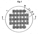
- Figure 1 is a plan view of a holder 1 for electroconductive contact units in a contact probe embodying the present invention.
- the holder 1 may consist of a disk having a diameter of eight inches (approximately 200 mm).
- An 8-inch wafer typically produces tens to hundreds of semiconductor chips.
- a 12-inch wafer (approximately 300 mm) typically produces thousands of semiconductor chips.
- the holder 1 for an electroconductive contact probe is circular in shape in plan view similarly as the wafer that is to be tested, and is provided with a plurality of holder holes 2 for receiving a plurality of electroconductive contact units at positions that correspond to the electrodes of the chips formed in the wafer as is the case with the prior art.
- the holder holes 2 are illustrated in a somewhat exaggerated manner, and are smaller in number than actually are.
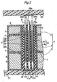
- Figure 2 is a fragmentary longitudinal sectional view taken along line II-II of Figure 1 showing exemplary electroconductive contact units embodying the present invention.
- three base plates 3, 4 and 5 having a same shape as seen in the plan view of Figure 1 are layered as an upper, middle and lower layer so as to form a three-layered holder 1 for an electroconductive contact probe.
- the base plates 3, 4 and 5 may be all made of a same material, and the mode of preparing a base plate 5 is described in the following with reference to Figure 3 .
- openings 5a are formed in a high strength base plate 5 by etching, laser, blanking or other mechanical process so as to correspond to the individual chips in the wafer that is to be tested.
- the high strength material for the base plate 5 may consist of metallic material having a low coefficient of thermal expansion such as invar and covar.
- the base plate may be made of ceramic, glass, silicon or other semiconductor or composite material having a desired mechanical properties.
- relatively thin film 6 (tens or hundreds of ⁇ m thick) made of such material as insulating plastic material is coated on the surface of the high strength base plate 5 having the openings 5a.
- the possible methods of coating may include calendar process, extrusion, immersion, spraying, spreading and electrostatic deposition.
- a holder hole forming portion 7 made of plastic material or the like that is suitable for machining or otherwise forming the holder holes for the contact probe is filled into each of the openings 5a.
- the film 6 demonstrates a high bonding strength with respect to the plastic material.
- a plurality of holder holes 2 for contact units are formed in each holder forming portion 7 so as to correspond to each individual chip.
- the base plate 5 is formed with a plurality of stepped holes each including a small diameter hole 2a and a large diameter hole 2b that are disposed coaxial to each other.
- the other base plates 3 and 4 are formed with a plurality of straight holes 2c and 2d each having a same diameter as the large diameter hole 2b.
- Each holder hole 2 is formed jointly by the corresponding stepped hole (2a and 2b) and straight holes (2c and 2d).
- the base plates 3, 4 and 5 are held in position in the laminated state as illustrated in Figure 2 by using threaded bolts or the like not shown in the drawing.
- the use of threaded bolts for securing the laminated assembly allows the assembly to be taken apart and reassembled with ease for maintenance and other purposes.
- each contact unit comprises an electroconductive coil spring 8 and pair of electroconductive contact needle members 9 and 10 provided on either end of the coil spring 8 with their free ends directed away from each other.
- One of the (or the lower) needle members 9 comprises a needle portion 9a having a pointed end that is directed downward in the drawing, a flange portion 9b having an enlarged diameter as compared with the needle portion 9a and a boss portion 9c projecting from the flange portion 9b away from the needle portion 9a (upward) all of which are disposed coaxial to one another.
- the other (or the upper) needle member 10 comprises a needle portion 10a having a pointed end that is directed upward in the drawing, a boss portion 10b having a smaller diameter than the needle portion 10a and a stem portion 10c projecting from the boss portion 10b away from the needle portion 10a (downward) all of which are again disposed coaxial to one another.
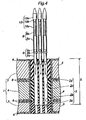
- the coil spring 8 comprises a closely wound portion 8a in a lower part thereof and a coarsely would portion 8b in an upper part thereof as seen in Figure 4 .
- the boss portion 9c of one of the needle member 9 fits into a coil end defined by the closely wound portion 8a, and the boss portion 10b of the other needle member 10 fits into the other coil end defined by the coarsely wound portion 8b.
- These boss portions 9b and 10c may be engaged by the corresponding ends of the coil spring 8 by virtue of the winding force of the coil spring or by solder. When solder is used, the fit between the boss portions 9b and 10c and the corresponding coil ends may be a loose one.
- the integrally joined assembly of the coil spring 8 and electroconductive needle members 9 and 10 is installed in the base plates (3, 4 and 5) by introducing it into the holder hole 2 as indicated by the arrow in Figure 4 .
- the contact unit may be used in an inverted orientation as illustrated in Figure 4 , as opposed to the orientation illustrated in Figure 2 . Even in such a case, by installing the assembly of the coil spring 8 and electroconductive needle members 9 and 10 as illustrated in Figure 4 , the assembly is prevented from coming off from the holder hole 2 by the flange portion 9b of one of the needle members 9 being engaged by the shoulder defined between the small diameter hole 2a and large diameter hole 2b.
- a circuit board 11 of the testing device is attached to the lower side of the contact probe, for instance by using threaded bolts with the stepped diameter hole of the holder 1 facing up and the straight hole of the holder hole 2 facing down.
- the circuit board 11 is provided with terminals 11a at positions corresponding to the needle members 10.
- the needle portion 10a of each needle member 10 engages the corresponding terminal 11a, and this prevents the assembly consisting of the coil spring 8 and needle members 9 and 10 from coming off from the holder hole 2 with the straight hole facing downward.
- the needle portion 9a of the upper needle member 9 projects upward.
- the contact probe By applying the contact probe toward a wafer 26 to be tested as indicated by the arrow in the drawing until the needle portions 9a come into contact with the corresponding electrodes 26a and the needle portions 9a and 10 are resiliently engage the corresponding electrodes 26a and terminals 11a.
- the wafer 26 can be electrically tested by using the contact probe in this manner.
- This arrangement enables the main component of the contact probe holder to be made of high strength base plates 3, 4 and 5, and the holder 1 may be provided with a level of mechanical strength comparable to the metallic material that is used for the high strength base plates 5.
- Forming the film 6 on the high strength base plate 5 can be most easily carried out by coating the film 6 over the entire surface of the high strength base plate 3, 4 and 5. If the film 6 is made of a highly insulating material, the entire surface of the high strength base plate 5 will be given with an insulating property.
- the film 6 defines a certain thickness on each of the front and back surfaces of the high strength base plate 5, but it is far less than the thickness of the plastic material that would cover the high strength base plate 5 by insert molding.
- the holder made by coating the film 6 over the high strength base plate 5 can be made thinner than the corresponding holder made by insert molding by the thickness of the plastic material that would cover the metallic reinforcing member for insert molding.
- This arrangement is particularly advantageous when a relatively thin base plate having a thickness in the order of 1 mm is used for a large holder (having a diameter in the range of 200 to 300 mm).
- the thickness of the plastic material covering the reinforcing metallic member inevitably accounts for a significant part of the total thickness when the thickness of the holder is as small as 1 mm. It would be extremely difficult to shave or otherwise remove the plastic layer to a thickness comparable to that of coated film, and would sharply increase the manufacturing cost.
- a very thin holder can be made relatively easily, and a rise in the manufacturing cost can be avoided.
- a slit 12 is formed between adjacent openings 5a of the high strength base plate 5.
- Each slit 12 extends along each side of each rectangular opening 5a in the illustrated embodiment, but may also be formed in other manner, for instance as a cross-shaped slit provided centrally of adjoining comers of the rectangular openings 5a.
- This structure can also be applied to a socket for mounting a chip on a circuit board.
- a socket of this type as the terminals of the chip get denser, the needle members (and coil springs) on the side of the socket get closer to one another, and the parts separating the adjacent holder holes 2 in each holder hole forming portion 7 become thinner. Therefore, when an electrostatic measure is required, the material for the holder hole forming portion 7 is required to have a favorably electrostatic property.
- readily available plastic materials which have a favorable electrostatic property are generally poor in electrically insulating properties.
- material having favorable electrically insulating properties as the material for the film 6, electric insulation in the holder can be ensured.
- a material having a favorable electrostatic property for the holder hole forming portion 7 By using a material having a favorable electrostatic property for the holder hole forming portion 7, a required electrostatic property can be ensured when the holder holes are densely arranged.
- a suitable material can be used for the holder hole forming portion 7 according to the particular application, and the range of application of the contact probe can be expanded.
- the contact probe holder was provided with a three-layered structure including three base plates 3, 4 and 5, but may also consist of a single base plate depending on the size and pitch of the holder holes.
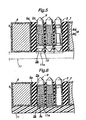
- Such a single layered structure is illustrated in Figure 5 .
- the base plate 5 shown in Figure 5 may be similar to the base plates of the previous embodiment, and the parts corresponding to those of the previous embodiment are denoted with like numerals without repeating the description of such parts.
- the contact probe holder illustrated in Figure 5 is provided with holder holes 2 each defined by a stepped diameter hole formed in a single base plate 5, and a coil spring 8 and a pair of electroconductive needle members 9 and 10 are received in each holder hole 2.
- holder holes 2 each defined by a stepped diameter hole formed in a single base plate 5, and a coil spring 8 and a pair of electroconductive needle members 9 and 10 are received in each holder hole 2.
- the coarsely wound portion 8b of the coil spring 8 is not required to be so long, and the holder 1 may consist of a single-layered structure including only one base plate 5. In such a case, the thickness of the holder 1 can be reduced even further.
- Electroconductive contact means on either end of each coil spring 8 consisted of a pair of needle members 9 and 10 in the foregoing embodiment, but the contact means on either end of each coil spring 8 facing the circuit board 11 may consist of a coil end 12 (the coil end of the coarsely wound portion in the illustrated embodiment) as illustrated in Figure 6 so as to apply this coil end 12 to the corresponding terminal 11a.
- the embodiment illustrated in Figure 6 consists of a single layer structure corresponding to the embodiment illustrated in Figure 5 , but may also consist of a three layer structure including three base plates 3, 4 and 5. In such a case also, the coil ends may be similarly adapted to be applied to the terminals 11a.
- the structure for the base plate according to the present invention is highly effective in increasing the mechanical strength of the base plates.
- thin insulating film 6 can be easily formed by spraying or dipping.
- the material for the hole forming portion in which the holder holes are formed may consist of plastic material suitable for forming such holes, the holder holes 2 can be formed at high precision without any difficulty, and a base plate having a generally high mechanical strength can be obtained with the added advantage of high productivity.
- the insulating film 6 was formed over the entire surface of the high strength base plate 5 in the illustrated embodiment, it is also possible to form film of different materials on the front and back surfaces of the high strength base plate 5 and the inner surface of the openings 5a.
- the film on the front and back surfaces of the high strength base plate 5 may consist of a highly insulating material while the film on the inner surface of the opening 5a may consist of a material demonstrating a high bonding force with respect to the holder hole forming portion 7, rather than a highly insulating property.
- the openings 5a can be formed in the high strength base plate 5 by etching, and by conducting etching from both directions as indicated by the arrows in Figure 7a , a ridge 13 that projects radially inward in an axially middle part of the openings and can serve as a means for preventing the dislodging of the holder hole forming portions 7 can be easily formed.
- This can be readily accomplished by using a base plate made from a silicon wafer, and anisotropically etching said inner circumferential surface of said opening, and no special work is required.
- the present invention when metallic material is used for the high strength base plate and plastic material is used for the holder hole forming portion, preferably by forming film on the inner circumferential surface of the opening to enhance a bonding force between the base plate and holder hole forming portion, there can be obtained an electroconductive contact probe holder having the high strength base plate and holder hole forming portions firmly joined together without requiring insert molding.
- This increases the proportion of the high strength base plate to the entire thickness of the holder, and the contact probe holder can be made almost as strong as the high strength base plate.
- the thickness of the high strength base plate can be minimized, and the favorable property of the material of the base plate can be favorably utilized.
- the holder holes for the contact probe can be formed in material suitable for forming such holes and a high positional accuracy can be achieved, the holder is highly suitable for use in contact probes for testing highly integrated chips.
- the opening is provided with a ridge or other projection for preventing the holder hole forming portion from coming off
- a recess corresponding to the projection is formed in the holder hole forming portion.
- the deformation of the holder as a whole owing to the thermal expansion of the high strength base plate may become too significant to be disregarded.
- This problem can be avoided by providing slits for accommodating deformation between adjacent openings that are provided in the high strength base plate in mutually parallel relationship.
- the slits accommodate the thermal deformation of the high strength base plate, and the positional accuracy of the contact units with respect to the individual chips in the wafer can be ensured.
- the slits can prevent the deformation of the holder into a dome-shape which otherwise could occur.
Landscapes
- Physics & Mathematics (AREA)
- General Physics & Mathematics (AREA)
- Testing Or Measuring Of Semiconductors Or The Like (AREA)
- Measuring Leads Or Probes (AREA)
Claims (6)
- Elektrisch leitfähige Kontaktsondenhalterung zum Tragen einer Mehrzahl von Kontakteinheiten, um ein Objekt zu kontaktieren, die umfasst:ein Basisplattenelement (5), das aus einem ersten Material hergestellt ist und mit einer Öffnung (5a) darin versehen ist, wobei das erste Material ein Element umfasst, das aus einer Gruppe ausgewählt ist, bestehend aus einem metallischen Material, Halbleitermaterial, keramischem Material und Glasmaterial, undein Halterungslochbildungselement (7), das aus einem zweiten Material hergestellt ist und in die Öffnung (5a) gefüllt ist, im Wesentlichen ohne sich außerhalb der Öffnung (5a) zu erstrecken, dadurch gekennzeichnet, dasseine Mehrzahl der Halterungslöchern (2) eine Dicke des Halterungslochbildungselements (7) passiert, wobei jedes vorgesehen ist, um darin eine Kontakteinheit aufzunehmen, so dass diese in das Halterungsloch (2) hinein und aus diesem heraus bewegbar ist, undein Film (6) über eine Innenumfangsfläche der Öffnung (5a) gebildet ist, wobei der Film (6) aus einem Material hergestellt ist, das eine Bindung zwischen dem Halterungslochbildungselement (7) und der Basisplatte (5) fördert.
- Elektrisch leitfähige Kontaktsondenhalterung nach Anspruch 1, wobei das zweite Material ein Kunststoffmaterial umfasst.
- Elektrisch leitfähige Kontaktsondenhalterung nach Anspruch 1, wobei der Film (6) aus einem Material hergestellt ist, das die elektrische Isolierung zwischen dem Halterungslochbildungselement (7) und der Basisplatte (5) fördert.
- Elektrisch leitfähige Kontaktsondenhalterung nach Anspruch 1, wobei ein Eingriffselement (13) auf einer Innenumfangsfläche der Öffnung (5a) gebildet ist.
- Elektrisch leitfähige Kontaktsondenhalterung nach Anspruch 4, wobei das Basisplattenelement (5) aus einem Siliciumwafer hergestellt ist und das Eingriffselement eine nach innen gerichtete Leiste (13) umfasst, die durch anisotropes Ätzen der Innenumfangsfläche der Öffnung (5a) gebildet ist.
- Elektrisch leitfähige Kontaktsondenhalterung nach Anspruch 1, wobei eine spannungsreduzierende Öffnung (12) der Öffnung (5a) benachbart gebildet ist, in die der Halterungslochbildungsabschnitt gefüllt ist.
Applications Claiming Priority (3)
| Application Number | Priority Date | Filing Date | Title |
|---|---|---|---|
| JP2002113485 | 2002-04-16 | ||
| JP2002113485 | 2002-04-16 | ||
| PCT/JP2003/004838 WO2003087853A1 (fr) | 2002-04-16 | 2003-04-16 | Support destine a un contact conducteur |
Publications (3)
| Publication Number | Publication Date |
|---|---|
| EP1496367A1 EP1496367A1 (de) | 2005-01-12 |
| EP1496367A4 EP1496367A4 (de) | 2005-09-07 |
| EP1496367B1 true EP1496367B1 (de) | 2015-09-16 |
Family
ID=29243355
Family Applications (1)
| Application Number | Title | Priority Date | Filing Date |
|---|---|---|---|
| EP03723132.1A Expired - Lifetime EP1496367B1 (de) | 2002-04-16 | 2003-04-16 | Halter für einen leitfähigen kontakt |
Country Status (7)
| Country | Link |
|---|---|
| US (1) | US7157922B2 (de) |
| EP (1) | EP1496367B1 (de) |
| KR (1) | KR100791137B1 (de) |
| CN (2) | CN100357744C (de) |
| AU (1) | AU2003235189A1 (de) |
| TW (1) | TWI290627B (de) |
| WO (1) | WO2003087853A1 (de) |
Families Citing this family (26)
| Publication number | Priority date | Publication date | Assignee | Title |
|---|---|---|---|---|
| KR100791136B1 (ko) * | 2002-04-16 | 2008-01-02 | 닛폰 하츠죠 가부시키가이샤 | 도전성 접촉자용 홀더 |
| GB2405249B (en) * | 2003-08-22 | 2007-03-07 | Ipwireless Inc | Holder for module and method therefor |
| JP4695337B2 (ja) * | 2004-02-04 | 2011-06-08 | 日本発條株式会社 | 導電性接触子および導電性接触子ユニット |
| JP4757531B2 (ja) * | 2005-04-28 | 2011-08-24 | 日本発條株式会社 | 導電性接触子ホルダおよび導電性接触子ユニット |
| US7154286B1 (en) * | 2005-06-30 | 2006-12-26 | Interconnect Devices, Inc. | Dual tapered spring probe |
| KR100679663B1 (ko) * | 2005-10-31 | 2007-02-06 | (주)티에스이 | 반도체 디바이스 테스트 소켓 |
| JP4884749B2 (ja) | 2005-10-31 | 2012-02-29 | 日本発條株式会社 | 導電性接触子ホルダの製造方法および導電性接触子ユニットの製造方法 |
| JP4905876B2 (ja) * | 2005-10-31 | 2012-03-28 | 日本発條株式会社 | 導電性接触子ホルダの製造方法および導電性接触子ホルダ |
| KR101077239B1 (ko) * | 2006-12-15 | 2011-10-27 | 니혼 하츠쵸 가부시키가이샤 | 도전성 접촉자 홀더 및 도전성 접촉자 유닛 |
| CN101315392A (zh) * | 2007-05-31 | 2008-12-03 | 佛山普立华科技有限公司 | 探针定位装置 |
| US7862391B2 (en) * | 2007-09-18 | 2011-01-04 | Delaware Capital Formation, Inc. | Spring contact assembly |
| US8633724B2 (en) | 2008-11-26 | 2014-01-21 | Nhk Spring Co., Ltd. | Probe-unit base member and probe unit |
| KR101415722B1 (ko) * | 2010-06-25 | 2014-07-25 | 니혼 하츠쵸 가부시키가이샤 | 콘택트 프로브 및 프로브 유닛 |
| JP5647869B2 (ja) * | 2010-11-18 | 2015-01-07 | 株式会社エンプラス | 電気接触子及び電気部品用ソケット |
| TW201231977A (en) * | 2011-01-20 | 2012-08-01 | Pleader Yamaichi Co Ltd | Structure of high-frequency vertical spring plate probe card |
| KR101552553B1 (ko) * | 2014-09-23 | 2015-10-01 | 리노공업주식회사 | 검사장치용 컨택트 프로브 |
| JP6411169B2 (ja) * | 2014-10-22 | 2018-10-24 | 株式会社日本マイクロニクス | 電気的接触子及び電気的接続装置 |
| CN107430151B (zh) * | 2015-03-31 | 2021-06-15 | 泰克诺探头公司 | 特别适用于高频应用的竖向接触探针和包含其的测试头 |
| PH12017000234A1 (en) * | 2016-09-02 | 2018-07-23 | Knight Auto Prec Engineering Pte Ltd | Handling assembly of semiconductor test equipment |
| CN109782041B (zh) * | 2019-02-20 | 2021-08-17 | 航天亮丽电气有限责任公司 | 一种具有防护功能的放置稳定的电力测量设备 |
| TWI679424B (zh) * | 2019-03-29 | 2019-12-11 | 矽品精密工業股份有限公司 | 檢測裝置及其製法 |
| US11150269B2 (en) * | 2019-08-15 | 2021-10-19 | Mpi Corporation | Probe head for high frequency signal test and medium or low frequency signal test at the same time |
| TWI807917B (zh) * | 2022-07-14 | 2023-07-01 | 中華精測科技股份有限公司 | 匹配型晶片測試插座 |
| CN117491836A (zh) | 2022-07-26 | 2024-02-02 | 迪科特测试科技(苏州)有限公司 | 测试装置 |
| CN117137323A (zh) * | 2023-09-13 | 2023-12-01 | 宁波霍科电器有限公司 | 一种冲奶机 |
| IT202300027405A1 (it) * | 2023-12-20 | 2025-06-20 | Technoprobe S P A | Testa di misura per un’apparecchiatura di test di dispositivi elettronici ad elevata frequenza |
Citations (1)
| Publication number | Priority date | Publication date | Assignee | Title |
|---|---|---|---|---|
| JP2001223247A (ja) * | 2000-02-10 | 2001-08-17 | Nhk Spring Co Ltd | 導電性接触子用支持体及びコンタクトプローブユニット |
Family Cites Families (17)
| Publication number | Priority date | Publication date | Assignee | Title |
|---|---|---|---|---|
| US4322682A (en) * | 1979-05-21 | 1982-03-30 | Everett/Charles Inc. | Vacuum actuated test head having programming plate |
| US4423376A (en) * | 1981-03-20 | 1983-12-27 | International Business Machines Corporation | Contact probe assembly having rotatable contacting probe elements |
| JPS60168062A (ja) | 1984-02-10 | 1985-08-31 | Yokowo Mfg Co Ltd | 集積回路のパタ−ン検査用ピンブロツク |
| JPH01213579A (ja) | 1988-02-22 | 1989-08-28 | Oki Electric Ind Co Ltd | 表面抵抗測定方法及びその装置 |
| JP2775267B2 (ja) * | 1988-11-10 | 1998-07-16 | 富士重工業株式会社 | 自動車用電動式パワステアリング装置の制御方法 |
| JPH02128961U (de) * | 1989-03-30 | 1990-10-24 | ||
| JP2538700B2 (ja) * | 1990-06-19 | 1996-09-25 | パトロマリサーチ有限会社 | 誤りファクシミリ繰り返し防止電話機 |
| JPH0451663U (de) * | 1990-09-06 | 1992-04-30 | ||
| JP3066784B2 (ja) * | 1992-12-14 | 2000-07-17 | 東京エレクトロン株式会社 | プローブカード及びその製造方法 |
| JP3394620B2 (ja) * | 1995-01-20 | 2003-04-07 | 株式会社日立製作所 | 探針組立体および検査装置 |
| JP2790074B2 (ja) | 1995-03-31 | 1998-08-27 | 日本電気株式会社 | プローブ装置 |
| US5804984A (en) | 1996-08-02 | 1998-09-08 | International Business Machines Corporation | Electronic component test apparatus with rotational probe |
| US6051982A (en) | 1996-08-02 | 2000-04-18 | International Business Machines Corporation | Electronic component test apparatus with rotational probe and conductive spaced apart means |
| WO1998011446A1 (en) | 1996-09-13 | 1998-03-19 | International Business Machines Corporation | Integrated compliant probe for wafer level test and burn-in |
| TW438977B (en) * | 1998-07-10 | 2001-06-07 | Nhk Spring Co Ltd | Electroconductive contact probe |
| JP4124520B2 (ja) * | 1998-07-30 | 2008-07-23 | 日本発条株式会社 | 導電性接触子のホルダ及びその製造方法 |
| US6641430B2 (en) * | 2000-02-14 | 2003-11-04 | Advantest Corp. | Contact structure and production method thereof and probe contact assembly using same |
-
2003
- 2003-04-16 CN CNB038085283A patent/CN100357744C/zh not_active Expired - Lifetime
- 2003-04-16 US US10/510,615 patent/US7157922B2/en not_active Expired - Lifetime
- 2003-04-16 TW TW092108968A patent/TWI290627B/zh not_active IP Right Cessation
- 2003-04-16 EP EP03723132.1A patent/EP1496367B1/de not_active Expired - Lifetime
- 2003-04-16 CN CNB2007101089309A patent/CN100543474C/zh not_active Expired - Lifetime
- 2003-04-16 AU AU2003235189A patent/AU2003235189A1/en not_active Abandoned
- 2003-04-16 WO PCT/JP2003/004838 patent/WO2003087853A1/ja not_active Ceased
- 2003-04-16 KR KR1020047016566A patent/KR100791137B1/ko not_active Expired - Fee Related
Patent Citations (1)
| Publication number | Priority date | Publication date | Assignee | Title |
|---|---|---|---|---|
| JP2001223247A (ja) * | 2000-02-10 | 2001-08-17 | Nhk Spring Co Ltd | 導電性接触子用支持体及びコンタクトプローブユニット |
Also Published As
| Publication number | Publication date |
|---|---|
| TWI290627B (en) | 2007-12-01 |
| US20050258843A1 (en) | 2005-11-24 |
| EP1496367A4 (de) | 2005-09-07 |
| AU2003235189A1 (en) | 2003-10-27 |
| TW200306426A (en) | 2003-11-16 |
| US7157922B2 (en) | 2007-01-02 |
| CN101059532A (zh) | 2007-10-24 |
| KR100791137B1 (ko) | 2008-01-02 |
| CN100357744C (zh) | 2007-12-26 |
| WO2003087853A1 (fr) | 2003-10-23 |
| CN1646923A (zh) | 2005-07-27 |
| CN100543474C (zh) | 2009-09-23 |
| KR20040105878A (ko) | 2004-12-16 |
| EP1496367A1 (de) | 2005-01-12 |
Similar Documents
| Publication | Publication Date | Title |
|---|---|---|
| EP1496367B1 (de) | Halter für einen leitfähigen kontakt | |
| US7239158B2 (en) | Holder for conductive contact | |
| US7898272B2 (en) | Probe card | |
| KR101921291B1 (ko) | 반도체소자 테스트소켓 | |
| US7306493B2 (en) | Interconnection device for a printed circuit board, a method of manufacturing the same, and an interconnection assembly having the same | |
| EP1496368B1 (de) | LEITFäHIGER KONTAKT | |
| US4623839A (en) | Probe device for testing an integrated circuit | |
| EP1950571A1 (de) | Verfahren zum herstellen eines leitfähigen kontakthalters und leitfähiger kontakthalter | |
| EP1400811B1 (de) | Haltekörperbaugruppe für einen leitfähigen kontaktor | |
| KR20170096480A (ko) | 프로브 카드 | |
| WO2010095521A1 (ja) | プローブカード | |
| US20220149555A1 (en) | Contactor block of self-aligning vertical probe card and manufacturing method therefor | |
| JPH05174923A (ja) | Icソケット | |
| JP2011153998A (ja) | コンタクトプローブおよびプローブユニット | |
| EP1555533B1 (de) | Prüfvorrichtung für Halbleiter und Verfahren zur Herstellung einer Prüfsonde | |
| KR200309258Y1 (ko) | 멀티소켓형 프로브카드 | |
| US20220155345A1 (en) | Contact terminal, inspection jig, and inspection device | |
| KR100493223B1 (ko) | 전자회로기판의검사프로브및검사방법 |
Legal Events
| Date | Code | Title | Description |
|---|---|---|---|
| PUAI | Public reference made under article 153(3) epc to a published international application that has entered the european phase |
Free format text: ORIGINAL CODE: 0009012 |
|
| 17P | Request for examination filed |
Effective date: 20041008 |
|
| AK | Designated contracting states |
Kind code of ref document: A1 Designated state(s): AT BE BG CH CY CZ DE DK EE ES FI FR GB GR HU IE IT LI LU MC NL PT RO SE SI SK TR |
|
| AX | Request for extension of the european patent |
Extension state: AL LT LV MK |
|
| A4 | Supplementary search report drawn up and despatched |
Effective date: 20050727 |
|
| REG | Reference to a national code |
Ref country code: DE Ref legal event code: R079 Ref document number: 60348046 Country of ref document: DE Free format text: PREVIOUS MAIN CLASS: G01R0001060000 Ipc: G01R0001067000 |
|
| GRAP | Despatch of communication of intention to grant a patent |
Free format text: ORIGINAL CODE: EPIDOSNIGR1 |
|
| RIC1 | Information provided on ipc code assigned before grant |
Ipc: G01R 1/067 20060101AFI20150325BHEP Ipc: G01R 1/073 20060101ALI20150325BHEP |
|
| INTG | Intention to grant announced |
Effective date: 20150408 |
|
| GRAS | Grant fee paid |
Free format text: ORIGINAL CODE: EPIDOSNIGR3 |
|
| GRAA | (expected) grant |
Free format text: ORIGINAL CODE: 0009210 |
|
| AK | Designated contracting states |
Kind code of ref document: B1 Designated state(s): DE IT |
|
| REG | Reference to a national code |
Ref country code: DE Ref legal event code: R096 Ref document number: 60348046 Country of ref document: DE |
|
| REG | Reference to a national code |
Ref country code: DE Ref legal event code: R097 Ref document number: 60348046 Country of ref document: DE |
|
| PLBE | No opposition filed within time limit |
Free format text: ORIGINAL CODE: 0009261 |
|
| STAA | Information on the status of an ep patent application or granted ep patent |
Free format text: STATUS: NO OPPOSITION FILED WITHIN TIME LIMIT |
|
| 26N | No opposition filed |
Effective date: 20160617 |
|
| PGFP | Annual fee paid to national office [announced via postgrant information from national office to epo] |
Ref country code: DE Payment date: 20200331 Year of fee payment: 18 |
|
| PGFP | Annual fee paid to national office [announced via postgrant information from national office to epo] |
Ref country code: IT Payment date: 20200312 Year of fee payment: 18 |
|
| REG | Reference to a national code |
Ref country code: DE Ref legal event code: R119 Ref document number: 60348046 Country of ref document: DE |
|
| PG25 | Lapsed in a contracting state [announced via postgrant information from national office to epo] |
Ref country code: DE Free format text: LAPSE BECAUSE OF NON-PAYMENT OF DUE FEES Effective date: 20211103 |
|
| PG25 | Lapsed in a contracting state [announced via postgrant information from national office to epo] |
Ref country code: IT Free format text: LAPSE BECAUSE OF NON-PAYMENT OF DUE FEES Effective date: 20200416 |
|
| PG25 | Lapsed in a contracting state [announced via postgrant information from national office to epo] |
Ref country code: IT Free format text: LAPSE BECAUSE OF NON-PAYMENT OF DUE FEES Effective date: 20210416 |