EP1555533B1 - Prüfvorrichtung für Halbleiter und Verfahren zur Herstellung einer Prüfsonde - Google Patents
Prüfvorrichtung für Halbleiter und Verfahren zur Herstellung einer Prüfsonde Download PDFInfo
- Publication number
- EP1555533B1 EP1555533B1 EP05250161A EP05250161A EP1555533B1 EP 1555533 B1 EP1555533 B1 EP 1555533B1 EP 05250161 A EP05250161 A EP 05250161A EP 05250161 A EP05250161 A EP 05250161A EP 1555533 B1 EP1555533 B1 EP 1555533B1
- Authority
- EP
- European Patent Office
- Prior art keywords
- view
- contact probe
- inspection device
- semiconductor inspection
- block parts
- Prior art date
- Legal status (The legal status is an assumption and is not a legal conclusion. Google has not performed a legal analysis and makes no representation as to the accuracy of the status listed.)
- Ceased
Links
Images
















Classifications
-
- H—ELECTRICITY
- H10—SEMICONDUCTOR DEVICES; ELECTRIC SOLID-STATE DEVICES NOT OTHERWISE PROVIDED FOR
- H10P—GENERIC PROCESSES OR APPARATUS FOR THE MANUFACTURE OR TREATMENT OF DEVICES COVERED BY CLASS H10
- H10P72/00—Handling or holding of wafers, substrates or devices during manufacture or treatment thereof
- H10P72/06—Apparatus for monitoring, sorting, marking, testing or measuring
- H10P72/0616—Monitoring of warpages, curvatures, damages, defects or the like
-
- G—PHYSICS
- G01—MEASURING; TESTING
- G01R—MEASURING ELECTRIC VARIABLES; MEASURING MAGNETIC VARIABLES
- G01R1/00—Details of instruments or arrangements of the types included in groups G01R5/00 - G01R13/00 and G01R31/00
- G01R1/02—General constructional details
- G01R1/06—Measuring leads; Measuring probes
- G01R1/067—Measuring probes
- G01R1/06711—Probe needles; Cantilever beams; "Bump" contacts; Replaceable probe pins
- G01R1/06716—Elastic
-
- G—PHYSICS
- G01—MEASURING; TESTING
- G01R—MEASURING ELECTRIC VARIABLES; MEASURING MAGNETIC VARIABLES
- G01R31/00—Arrangements for testing electric properties; Arrangements for locating electric faults; Arrangements for electrical testing characterised by what is being tested not provided for elsewhere
- G01R31/28—Testing of electronic circuits, e.g. by signal tracer
- G01R31/2851—Testing of integrated circuits [IC]
- G01R31/2886—Features relating to contacting the IC under test, e.g. probe heads; chucks
-
- Y—GENERAL TAGGING OF NEW TECHNOLOGICAL DEVELOPMENTS; GENERAL TAGGING OF CROSS-SECTIONAL TECHNOLOGIES SPANNING OVER SEVERAL SECTIONS OF THE IPC; TECHNICAL SUBJECTS COVERED BY FORMER USPC CROSS-REFERENCE ART COLLECTIONS [XRACs] AND DIGESTS
- Y10—TECHNICAL SUBJECTS COVERED BY FORMER USPC
- Y10T—TECHNICAL SUBJECTS COVERED BY FORMER US CLASSIFICATION
- Y10T29/00—Metal working
- Y10T29/49—Method of mechanical manufacture
- Y10T29/49002—Electrical device making
- Y10T29/49117—Conductor or circuit manufacturing
- Y10T29/49124—On flat or curved insulated base, e.g., printed circuit, etc.
- Y10T29/49155—Manufacturing circuit on or in base
- Y10T29/49165—Manufacturing circuit on or in base by forming conductive walled aperture in base
Definitions
- the present invention generally relates to a semiconductor inspection device and a method for manufacturing a contact probe, and more particularly, to a semiconductor inspection device including a contact probe that is electrically connected to a terminal part of an electronic device when inspecting the electronic device and a method for manufacturing the contact probe.
- the BGA (Ball Grid Array) and the CSP (Chip Size Package) have its bottom surface part provided with a grid-like array of solder balls.
- the pitch of the solder balls can be arranged with a narrower pitch. This enables high densification and size-reduction of the semiconductor device.
- a reliability inspection is performed on the semiconductor device before shipment. In the reliability test, the semiconductor device is tested by actually supplying a test signal to the semiconductor device. Accordingly, contact probes connected to a tester is connected to the solder balls of the semiconductor device.
- Fig.1 is a drawing showing a contact probe according to a conventional technology.
- a contact probe 10 being generally referred to as a pogo pin, is illustrated in Fig.1 .
- the contact probe 10 mainly includes a shaft part 11, an upper part plunger 12 for connecting to the solder balls of the BGA, a lower part plunger 13 for connecting to an inspection apparatus (tester), and coil springs 14.
- the coil springs 14 are disposed between the upper and lower plungers 12, 13.
- the coil springs 14 allow the upper part plunger 12 to be displaceable in a vertical direction (arrow direction in Fig.1 ) with respect to the lower part plunger 13.
- a housing 15 is formed with a through-hole for disposing the contact probe 10 therein (See, for example, Japanese Laid-Open Patent Application No.2001-255340 ).
- FIG.2 is a drawing showing a wire-shaped contact probe according to a conventional technology.
- a contact probe 20 includes a soft core 21 and a hard shell 22 disposed in a manner encasing the soft core 21.
- the soft core 21 is formed with a wire bonding technique.
- the hard shell 22 is formed with a plating method (See, for example, Japanese Laid-Open Patent Application No. 11-126800 ).
- the contact probe 10 since the contact probe 10 employs mechanical components such as the coil springs, the contact probe 10 has a difficulty in disposing the contact probe 10 in a narrow pitch. Furthermore, since the contact probe 10 is hand-manufactured, the contact probe 10 has poor process precision, requires large manufacture cost, and its unable to be mass-produced. In addition, the contact probe 10 requiring a large number of components further increases the manufacture cost.
- the contact probe 20 formed by the wire-bonding technique it is difficult to disposed the contact probe 20 in a narrow pitch since the contact probe 20 is formed with a complicated shape. Furthermore, owing to the wire shape of the contact probe 20, the contact probe 20 is liable to be subject to problems as permanent set in fatigue and/or plastic deformation.
- US-B-6359455 discloses a device having a contact probe supported a spiral arm acting as volute like plate. The entire contact probe is formed from nickel or a nickel alloy.
- JP07007052A Another known semi-conductor inspection device is disclosed in JP07007052A . This discloses a contact probe supported by a cantilever beam structure formed on a silicon substrate.
- the invention provides a semiconductor inspection device according to claim 1.
- the block parts may be disposed on the silicon substrate in a spiral-like manner when observed from a plan view direction.
- the holding part may include a frame body encompassing the block parts, wherein the frame body is integrally formed with at least one of the block parts of the contact probe, wherein the block parts each have a bottom face part that shares a same plane with respect to a bottom face part of the frame body.
- the present invention provides a method of manufacturing a contact probe according to claim 4.
- the present invention provides a method of manufacturing a contact probe including first to fourth block parts, the method including the steps of: a) forming a first resist film on a portion of the silicon substrate corresponding to the holding part and a portion of the silicon substrate corresponding to a position of the first block part; b) forming a second resist film on the first resist flim and a portion of the silicon substrate corresponding to a position of the second block part, the second resist film having a property different from that of the first resist flim; c-1) forming a third resist film on the second resist film and a portion of the silicon substrate corresponding to a position of the third block part, the third resist film having a property different from that of the second resist film; c-2) forming a fourth resist film on the third resist flim and a portion of the fourth block part, the fourth resist film having a property different from that of the third resist; d) etching a first area to a first depth by using the fourth resist film as a mask and then removing
- the holding part may include a frame body encompassing the first to fourth block parts, wherein the frame body may be integrally formed with at least one of the first to fourth block parts of the contact probe.
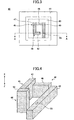
- Fig.3 is a plan view showing the semiconductor inspection device according to the first embodiment of the present invention
- Fig.4 is a perspective view of a contact probe shown in Fig.3
- Fig.5 is a cross-sectional view of the semiconductor inspection device along line A-A of Fig.3 .
- the arrow direction Z-Z in Fig.4 indicates a vertical direction.
- Numeral 60B shown in Fig.5 indicates a back face of a contact probe 45 and a holding part 41 (hereinafter referred to as "rear face 60B").
- a semiconductor inspection device 40 mainly includes the holding part 41, the contact probe 45, and a measuring part 58 (see Fig.5 ).
- the contact probe 45 and the holding part 41 are integrally formed.
- the holding part 41 is formed as a frame body in a manner encompassing the contact probe 45, a through part 83 is formed between the contact probe 45 and the holding part 41. It is to be noted that, although not shown in the drawing, plural contact probes 45 are disposed in grid-like manner in the semiconductor inspection device 40.
- the contact probe 45 mainly includes plural column parts (first column part 46 to fourth column part 49), a conductive layer (conductive metal layer) 52, and a through-hole electrode 55.
- the first-fourth column parts 46-49 having different height, are disposed in continuation, in which the first column part 46 is the most highest column part, the second column part 47 is the second highest column part, the third column part 48 is the third highest column part, and the fourth column part 49 is the fourth highest column part. Furthermore, the first-fourth column parts 46-49 each have a bottom face part (rear face 60B) which shares a same plane.
- the first-fourth column parts 46-49 are arranged forming a spiral-like shape.
- the contact probe 45 is supported in a cantilever manner by the holding part 41 via the fourth column part 49.
- the contact probe 45 is able to attain a spring-like property with respect to the frame body-shaped holding part 41. Accordingly, when the contact probe 45 is contacted to a terminal part 57 of an electronic device 56, plastic deformation of the contact probe 45 can be reduced, thereby extending the lifetime of the contact probe 45. Furthermore, since the first-fourth column parts 46-49 support each other by arranging the first-fourth column parts 46-49 in the spiral-like manner, the strength of the contact probe 45 can be increased.
- the conductive layer 52 is formed at least on the surfaces of the first-fourth column parts 46-49.
- the fourth column part 49 which is lowest in height, includes the through-hole electrode 55 being formed in a through-hole penetrating the fourth column part 49 in direction Z-Z.
- the through-hole electrode 55 is formed simultaneously with the forming of the conductive layer 52.
- the through-hole electrode 55 serves to electrically connect the rear face 60B and the conductive layer 52.
- the measuring part 58 is electrically connected to the through-hole electrode 55.
- the measuring part 58 is used in inspecting an electronic device 56 based on input-output signals from the electronic device 56.
- the electronic device 56 being the target for inspection, other semiconductor elements may be employed as alternatives of the CSP or the BGA.
- the inspection of the electronic device 56 is performed by abutting the terminal part 57 of the electronic device 56 to the conductive layer 52 formed at an upper face part of the first column part 46 and electrically connecting the measuring part 58 and the electronic device 56 via the through-hole electrode 55.
- the contact probe 45 and the holding part 41 is integrally formed with a single silicon substrate.
- a high precision processing technology used in processing semiconductor devices is employed (described in detail below). Accordingly, process precision can be improved, thereby enabling the contact probes 45 to be disposed in a narrower pitch compared to the conventional contact probe.
- the contact probes 45 can be mass produced at low cost. Furthermore, since a silicon substrate is employed as the material of the contact probe 45, plastic deformation of the contact probe 45 can be prevented more effectively compared to the conventional contact probe.
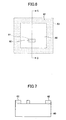
- Fig.6 is a plan view (part 1) showing a process of the manufacture method of the semiconductor inspection device according to the first embodiment of the present invention.
- Fig.7 is a cross-sectional view of the configuration shown in Fig.6 along line C-C of Fig.6 .
- a first resist film 62 is formed on an area 63 of the silicon substrate 60 corresponding to the holding part 41 and on an area 61 of the silicon substrate 60 corresponding to the first column part 46.
- a liquid resist containing, for example, a phenolic resin as a main component, a melamine and/or epoxy resin as a sub-component, and a photosensitive agent may be employed, in which the resist is coated and is then heated.
- Fig.8 is a plan view (part 2) showing a process of the manufacture method of the semiconductor inspection device according to the first embodiment of the present invention.
- Fig.9 is a cross-sectional view of the configuration shown in Fig.8 along line C-C of Fig.6 .
- a second resist film 65 having a property different from that of the first resist film 62, is formed on an area 64 of the silicon substrate 60 corresponding to the second column part 47 and on the first resist film 62.
- a liquid resist containing, for example, a novolac resin and/or naphthoquinone diazide dielectric as a main component may be employed.
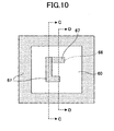
- Fig.10 is a plan view (part 3) showing a process of the manufacture method of the semiconductor inspection device according to the first embodiment of the present invention.
- Fig.11 is a cross-sectional view of the configuration shown in Fig.10 along line C-C of Fig.10 .
- Fig.12 is a cross-sectional view of the configuration shown in Fig.10 along line D-D of Fig.10 .
- a third resist film 67 having a property different from that of the second resist film 65, is formed on an area 66 of the silicon substrate 60 corresponding to the third column part 48 and on the second resist film 65.
- a liquid resist containing, for example, a phenolic resin as a main component, a melamine and/or epoxy resin as a sub-component, and a photosensitive agent may be employed, in which the resist is coated and is then heated.
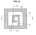
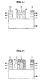
- Fig.13 is a plan view (part 4) showing a process of the manufacture method of the semiconductor inspection device according to the first embodiment of the present invention.
- Fig.14 is a cross-sectional view of the configuration shown in Fig.13 along line C-C of Fig.6 .
- Fig.15 is a cross-sectional view of the configuration shown in Fig.13 along line E-E of Fig.13 .
- a fourth resist film 71 having a property different from that of the third resist film 67, is formed on an area 72 of the silicon substrate 60 corresponding to the fourth column part 49 and on the third resist film 67.
- the fourth resist layer 71 at the area 62 corresponding to the fourth column part 49 and the fourth resist layer 71 situated at the area 63 corresponding to the holding part 41 are integrally formed in a continuing manner.
- the fourth column part 49 can be supported by the holding part 41 during a first etching process using the fourth resist layer 71 as a mask.
- a liquid resist containing, for example, a novolac resin and/or naphthoquinone diazide dielectric as a main component may be employed.
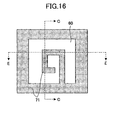
- Fig.16 is a plan view (part 5) showing a process of the manufacture method of the semiconductor inspection device according to the first embodiment of the present invention.
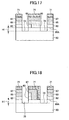
- Fig.17 is a cross-sectional view of the configuration shown in Fig.16 along line C-C of Fig.16 .
- Fig.18 is a cross-sectional view of the configuration shown in Fig.16 along line E-E of Fig.16 .
- H1 in Figs.17 and 18 indicates the depth of a groove part 73 formed by a first etching process (hereinafter referred to depth H1).
- the first etching process using the fourth resist layer 71 as a mask is performed on the silicon substrate 60 to form the groove part 73 having a depth H1 with respect to surface 60A of the silicon substrate 60. Then, the fourth resist film 71 is removed.
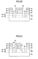
- Fig.19 is a plan view (part 6) showing a process of the manufacture method of the semiconductor inspection device according to the first embodiment of the present invention.
- Fig.20 is a cross-sectional view of the configuration shown in Fig.19 along line C-C of Fig.19 .
- Fig.21 is a cross-sectional view of the configuration shown in Fig.19 along line E-E of Fig.19 .
- H2 in Figs.20 and 21 indicates an etching depth formed by a second etching process (hereinafter referred to depth H2).
- the second etching process using the third resist layer 67 as a mask is performed on the silicon substrate 60 to form a groove part 75 having a depth (H1+H2) with respect to surface 60A of the silicon substrate 60, and a step part 76 of area 72 corresponding to the fourth column part 49.
- the step part 75 is formed as a step having a depth H2 with respect to surface 60A of the silicon substrate 60.
- the third resist film 67 is removed.
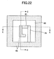
- Fig.22 is a plan view (part 7) showing a process of the manufacture method of the semiconductor inspection device according to the first embodiment of the present invention.
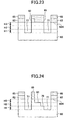
- Fig.23 is a cross-sectional view of the configuration shown in Fig.22 along line C-C of Fig.22 .
- Fig.24 is a cross-sectional view of the configuration shown in Fig.22 along line E-E of Fig.22 .
- H3 in Figs.23 and 24 indicates an etching amount of a third etching process (etching depth, hereinafter referred to as "depth H3").
- the third etching process using the second resist layer 65 as a mask is performed on the silicon substrate 60 to form a groove part 77 having a depth (H1+H2+H3) with respect to surface 60A of the silicon substrate 60, a step part 79 having a depth (H2+H3) in the area 72 corresponding to the fourth column part 49, and a step part 81 having a depth H3 in the area 66 corresponding to the third column part 48.
- the second resist film 65 is removed.
- Fig.25 is a plan view (part 8) showing a process of the manufacture method of the semiconductor inspection device according to the first embodiment of the present invention.
- Fig.26 is a cross-sectional view of the configuration shown in Fig.25 along line C-C of Fig.25 .
- Fig.27 is a cross-sectional view of the configuration shown in Fig.25 along line E-E of Fig.25 .
- H4 in Figs.26 and 27 indicates an etching amount of a fourth etching process (etching depth, hereinafter referred to as "depth H4").
- the fourth etching process using the first resist layer 62 as a mask is performed on the silicon substrate 60 to form the through part 83, the holding part 41, the fourth column part 49 including a step having a depth (H2+H3+H4) with respect to an upper face 41A of the holding part (silicon holding part) 41 in the area 72, the third column part 48 including a step having a depth (H3+H4) in the area 66, the second column part 47 including a step having a depth (H4) in the area 64, and the first column part 46.
- An upper face 46A of the first column part 46 is disposed sharing a common plane with the upper face 41A of the holding part 41.
- Fig.28 is a plan view (part 9) showing a process of the manufacture method of the semiconductor inspection device according to the first embodiment of the present invention.
- Fig.29 is a cross-sectional view of the configuration shown in Fig.28 along line A-A of Fig.28 .
- Fig.30 is a cross-sectional view (part 1) showing a process of the manufacture method of the semiconductor inspection device according to the first embodiment of the present invention.
- a resist film 91 having an opening part 92 for forming a through-hole 94 is formed so that the through-hole electrode 55 can be formed in the fourth column part 49.
- an etching process using the resist film 91 as a mask is performed to form the through-hole 94.
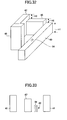
- Fig.31 is a plan view (part 10) showing a process of the manufacture method of the semiconductor inspection device according to the first embodiment of the present invention.
- Fig.32 is a perspective view of the first-fourth column parts 46-49 formed in an area G shown in Fig.31 .
- Fig.33 is a cross-sectional view of the configuration shown in Fig.31 along line A-A of Fig.31 .
- the resist film 91 is removed.
- Fig.34 is a plan view (part 11) showing a process of the manufacture method of the semiconductor inspection device according to the first embodiment of the present invention.
- Fig.35 is a cross-sectional view of the configuration shown in Fig.34 along line A-A of Fig.34 .
- a seed layer 95 used when forming a plating film on the configuration shown in Fig.33 and inside the through-hole 94.
- the seed layer 95 may be formed with, for example, a sputter method or a CVD method.
- a Ti film, a W film, or a Cr film may be employed for the seed layer 95.
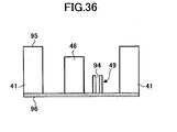
- Fig.36 is a cross-sectional view is a cross-sectional view (part 2) showing a process of the manufacture method of the semiconductor inspection device according to the first embodiment of the present invention.
- the seed layer 96 is adhered to the rear face 60B of the contact probe 45 and the holding part 41.
- a conductive tape having CU as a base material may be employed as the seed layer 96.
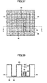
- Fig.37 is a plan view (part 12) showing a process of the manufacture method of the semiconductor inspection device according to the first embodiment of the present invention.
- Fig.38 is a cross-sectional view of the configuration shown in Fig.37 along line A-A of Fig.37 .
- electricity is supplied from the seed layer 95 adhered to the rear face 60B of the contact probe 45 and the holding part 41, and then a plating process is performed to form a plating film 98 at the upper and side faces of the first-fourth column parts 46-49.
- the through-hole electrode 55 including the seed layer 95 and the plating film 98 is formed inside the through-hole 94, and the conductive layer 52 including the seed layer 95 and the plating film 98 is formed on the contact probe 45 and the holding part 41.
- a film including a Ni alloy, Cu, and/or gold may be employed as the plating film 98.
- Fig.39 is a plan view (part 13) showing a process of the manufacture method of the semiconductor inspection device according to the first embodiment of the present invention.
- Fig.40 is a cross-sectional view of the configuration shown in Fig.39 along line A-A of Fig.39 .
- the seed layers 95 and 96 and the plating film 98 (conductive layer 52) except for those formed on the surface of the contact probe 45 and the through-hole electrode 55 are removed, thereby completing the manufacturing of the semiconductor inspection device 40 including the contact probe 45 according to the first embodiment of the present invention.
- a film of conductive polymer such as polypyrrole or polyacetylene, may be employed as an alternative for the conductive metal material of the conductive layer 52.
- The'through-hole electrode 55 may be formed with the conductive polymer.
- a polypyrrole film can be formed by coating with a polypyrrole solution.
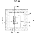
- Fig.41 is a plan view showing the semiconductor inspection device according to the second embodiment of the present invention
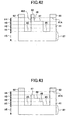
- Fig.42 is a cross-sectional view of the configuration shown in Fig.41 along line C-C of Fig.41
- Fig.43 is a cross-sectional view of the configuration shown in Fig.41 along line E-E of Fig.41
- the method of manufacturing the semiconductor inspection device including the contact probe according to the second embodiment of the present invention is a modified example of the method of manufacturing the semiconductor inspection device 40 including the contact probe 45 according to the first embodiment of the present invention. Therefore, in Figs.41 to 43 , like components are denoted by like numerals as of Figs.25 to 27 .
- a plate member 87 having a thickness H5 and the holding part 41 are formed in addition to the formation of the first-fourth column parts 46-49. Furthermore, a groove part 85 is formed between the first-fourth column parts 46-49 and the holding part 41.
- the plate member 87 is removed by polishing or etching. After the plate member 87 is removed, the conductive layer 52 and the through-hole electrode 55 are formed by executing the above-described processes illustrated with Figs.28-40 , thereby completing the manufacturing of the semiconductor inspection device 40.
- the strength of the semiconductor inspection device 40 can be maintained when the semiconductor inspection device 40 is transported to or from processing apparatuses, such as a photolithography apparatus or an etching apparatus, during the manufacture processes.
- Fig.44 is a plan view showing the semiconductor inspection device according to the third embodiment of the present invention
- Fig.45 is a perspective view of a contact probe shown in Fig.44
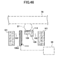
- Fig.46 is a cross-sectional view of the semiconductor inspection device along line I-I of Fig.44 . It is to be noted that the arrow direction Z-Z in Fig.45 indicates a vertical direction.
- a semiconductor inspection device 100 mainly includes a holding part 101, a contact probe 105, and a measuring part 58 (see Fig.46 ).
- the contact probe 105 and the holding part 101 are integrally formed.
- the holding part 101 is formed as a frame body in a manner encompassing the contact probe 105.
- the holding part 101 is integrally formed with a first column part 106 included in the contact probe 105.
- a through part 102 is formed between the contact probe 105 and the holding part 101. This allows the contact probe 105 to be supported by the holding part 101 in a flexible state.
- the contact probe 105 is able to attain a spring-like property with respect to the holding part 101. Accordingly, when the contact probe 105 is contacted to the terminal part 57 of the electronic device 56, plastic deformation of the contact probe 105 can be reduced, thereby extending the lifetime of the contact probe 105.
- the contact probe 105 includes plural column parts (first column part 106 to fourth column part 109), a conductive layer (conductive metal layer) 114, and a through-hole electrode 111.
- the first-fourth column parts 106-109 having different height, are disposed in continuation, in which the first column part 106 is the most highest column part, the second column part 107 is the second highest column part, the third column part 108 is the third highest column part, and the fourth column part 109 is the fourth highest column part.
- the first-fourth column parts 106-109 are arranged forming a spiral-like shape. Furthermore, the first-fourth column parts 106-109 each have bottom face parts 106A-109A which share a same plane.
- the bottom face parts 106A-109A of the first-fourth column parts 106-109 are respectively formed with the conductive metal layer 114 for electrically connecting with the terminal part 57 of the electronic device 56.
- the first column part 106 includes the through-hole electrode 111 being formed in a through-hole penetrating the first column part 106 in direction Z-Z.
- the through-hole electrode 111 serves to electrically connect a surface part of the first column part 106 and the conductive layer 114.
- the through-hole electrode 111 is formed simultaneously with the forming of the conductive layer 114.
- the measuring part 58 is electrically connected to the through-hole electrode 111.
- the measuring part 58 is used in inspecting the electronic device 56 based on input-output signals from the electronic device 56.
- the inspection of the electronic device 56 is performed by abutting the terminal part 57 of the electronic device 56 to a face of the fourth column part at which the conductive layer 114 is formed and electrically connecting the measuring part 58 and the electronic device 56 via the through-hole electrode 111.
- the contact probe(s) 105 can be disposed in a narrow pitch and be mass produced at low cost.
- Fig.47 is a plan view (part 1) showing a process of the manufacture method of the semiconductor inspection device according to the third embodiment of the present invention.
- Fig.48 is a cross-sectional view of the configuration shown in Fig.47 along line I-I of Fig.47 .
- a first resist film 123 is formed on an area 121 of the silicon substrate 120 corresponding to the holding part 101 and on an area 122 of the silicon substrate 120 corresponding to the first column part 106.
- a opening part 124 is formed in the first resist film 123 disposed in the area 122 corresponding to the first column part 106.
- the opening part 124 is provided for forming a through-hole afterwards in the first column part 106.
- a liquid resist containing, for example, a phenolic resin as a main component, a melamine and/or epoxy resin as a sub-component, and a photosensitive agent may be employed, in which the resist is coated and is then heated.
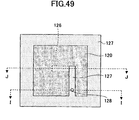
- Fig.49 is a plan view (part 2) showing a process of the manufacture method of the semiconductor inspection device according to the third embodiment of the present invention.
- Fig.50 is a cross-sectional view of the configuration shown in Fig.49 along line I-I of Fig.49 .
- Fig.51 is a cross-sectional view of the configuration shown in Fig.49 along line J-J of Fig.49 .
- a second resist film 107 having a property different from that of the first resist film 123 and thus having an opening part 128 formed thereto, is formed on an area 126 of the silicon substrate 120 corresponding to the second column part 107 and on the first resist film 123.
- a liquid resist containing, for example, a novolac resin and/or naphthoquinone diazide dielectric as a main component may be employed.
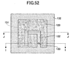
- Fig.52 is a plan view (part 3) showing a process of the manufacture method of the semiconductor inspection device according to the third embodiment of the present invention.
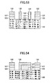
- Fig.53 is a cross-sectional view of the configuration shown in Fig.52 along line I-I of Fig.52 .
- Fig.54 is a cross-sectional view of the configuration shown in Fig.52 along line J-J of Fig.52 .
- a third resist film 108 having a property different from that of the second resist film 127, is formed on an area 131 of the silicon substrate 120 corresponding to the third column part 108 and on the second resist film 127.
- the third resist film 132 is formed with an opening part 133 which exposes the opening part 128.
- a liquid resist containing, for example, a phenolic resin as a main component, a melamine and/or epoxy resin as a sub-component, and a photosensitive agent may be employed, in which the resist is coated and is then heated.
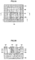
- Fig.55 is a plan view (part 4) showing a process of the manufacture method of the semiconductor inspection device according to the third embodiment of the present invention.
- Fig.56 is a cross-sectional view of the configuration shown in Fig.55 along line I-I of Fig.55 .
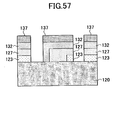
- Fig.57 is a cross-sectional view of the configuration shown in Fig.55 along line J-J of Fig.55 .
- a fourth resist film 109 having a property different from that of the third resist film 132, is formed on an area 136 of the silicon substrate 120 corresponding to the fourth column part 109 and on the third resist film 132.
- the fourth resist film 137 is formed with an opening part 138 which exposes the opening part 133.
- a liquid resist containing, for example, a novolac resin and/or naphthoquinone diazide dielectric as a main component may be employed.
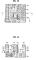
- Fig.58 is a plan view (part 5) showing a process of the manufacture method of the semiconductor inspection device according to the third embodiment of the present invention.
- Fig.59 is a cross-sectional view of the configuration shown in Fig.58 along line I-I of Fig.58 .
- Fig.60 is a cross-sectional view of the configuration shown in Fig.58 along line J-J of Fig.58 .
- L1 in Figs.58 to 60 indicates the depth of a groove part 141 formed by a first etching process (etching depth, hereinafter referred to as depth L1).
- the first etching process using the fourth resist layer 137 as a mask is performed on the silicon substrate 120 to form the groove part 141 having a depth L1 with respect to the surface of the silicon substrate 120. Then, the fourth resist film 137 is removed.
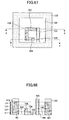
- Fig.61 is a plan view (part 6) showing a process of the manufacture method of the semiconductor inspection device according to the third embodiment of the present invention.
- Fig.62 is a cross-sectional view of the configuration shown in Fig.61 along line I-I of Fig.61 .
- Fig.63 is a cross-sectional view of the configuration shown in Fig.61 along line J-J of Fig.61 .
- L2 in Figs.61 to 63 indicates an etching amount depth formed by a second etching process (etching depth, hereinafter referred to as depth L2).
- the second etching process using the third resist layer 132 as a mask is performed on the silicon substrate 120 to form a groove part 146 having a depth (L1+L2) with respect to the surface of the silicon substrate 120, and a step part 142 of area 136 corresponding to the fourth column part 109.
- the step part 142 is formed as a step having a depth L2 with respect to the surface of the silicon substrate 120.
- the third resist film 132 is removed.
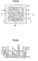
- Fig.64 is a plan view (part 7) showing a process of the manufacture method of the semiconductor inspection device according to the third embodiment of the present invention.
- Fig.65 is a cross-sectional view of the configuration shown in Fig.64 along line I-I of Fig.64 .
- Fig.66 is a cross-sectional view of the configuration shown in Fig.64 along line J-J of Fig.64 .
- L3 in Figs.64 to 66 indicates an etching amount of a third etching process (etching depth, hereinafter referred to as "depth L3").
- the third etching process using the second resist layer 127 as a mask is performed on the silicon substrate 120 to form a groove part 152 having a depth (L1+L2+L3) with respect to the surface of the silicon substrate 120, a step part 148 having a depth (L2+L3) in the area 136 corresponding to the fourth column part 109, and a step part 149 having a depth L3 in the area 131 corresponding to the third column part 108.
- the second resist film 127 is removed.
- Fig.67 is a plan view (part 8) showing a process of the manufacture method of the semiconductor inspection device according to the third embodiment of the present invention.
- Fig.68 is a cross-sectional view of the configuration shown in Fig.67 along line I-I of Fig.67 .
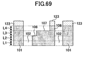
- Fig.69 is a cross-sectional view of the configuration shown in Fig.67 along line J-J of Fig.67 .
- L4 in Figs.67 to 69 indicates an etching amount of a fourth etching process (etching depth, hereinafter referred to as "depth L4").
- the fourth etching process using the first resist layer 123 as a mask is performed on the silicon substrate 120 to form the through part 102, the holding part 101, the fourth column part 109 including a step having a depth (L2+L3+L4) with respect to an upper face of the holding part 101 in the area 136, the third column part 108 including a step having a depth (L3+L4) with respect to the upper face of the holding part 101 in the area 131, the second column part 107 including a step having a depth (L4) with respect to the upper face of the holding part 101 in the area 126, and the first column part 106 having an upper face that shares a same plane with respect to the upper surface of the holding part 101. Furthermore, the first column part 106 is provided with a through-hole 125 for forming the through-hole electrode 111.
- the step having the depth L4 is formed between the first column part 106 and the second column part 107
- the step having the depth L3 is formed between the second column part 107 and the third column part 108
- the step having the depth L2 is formed between the third column part 108 and the fourth column part 109.
- L1 may be set to, for example, 50 ⁇ m.
- the widths of the first-fourth column parts 106-109 may be formed, for example, in sizes ranging approximately between 15-50 ⁇ m.
- Fig.70 is a plan view (part 9) showing a process of the manufacture method of the semiconductor inspection device according to the third embodiment of the present invention.
- Fig.71 is a cross-sectional view of the configuration shown in Fig.70 along line I-I of Fig.70 .
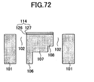
- Fig.72 is a cross-sectional view of the configuration shown in Fig.70 along line J-J of Fig.70 .
- the conductive metal layer 114 including a seed layer 126 and a metal plating film 127 is formed on the bottom face parts 106A-109A of the first-fourth column parts 106-109, and the through-hole electrode 111 including the seed layer 126 and the metal plating film 127 is formed in the through-hole 125.
- a Ti film, a W film, or a Cr film may be employed as the seed layer 126.
- a film including, for example, a Ni alloy, Cu, and/or gold may be employed as the plating film 127. It is to be noted that, since the processes for forming the conductive metal layer 114 and the through-hole 111 are the same as that of the first embodiment, further description thereof is omitted.
- the semiconductor inspection device 100 in manufacturing the semiconductor inspection device 100 with the above-described manufacturing processes, process precision can be improved by employing such photo-etching technique used for processing semiconductor devices or the like, to thereby enable the contact probe(s) 105 to be arranged in a narrower pitch than the conventional contact probe(s).
- the contact probe 105 having little plastic deformation can be mass-produced at low cost.
- the fourth column part 109 may be integrally formed with the holding part 101.
- the position of the through-hole electrode (55, 111) is not limited to the position described in the first-third embodiments, but may be formed at any one of the plural column parts.
- the present invention provides a semiconductor inspection apparatus including a contact probe and a method for manufacturing the contact probe for improving process precision, enabling contact probes to be disposed in a narrow pitch, and allowing contact probes to be mass produced at low cost.
Landscapes
- Physics & Mathematics (AREA)
- General Physics & Mathematics (AREA)
- Testing Or Measuring Of Semiconductors Or The Like (AREA)
- Measuring Leads Or Probes (AREA)
- Testing Of Individual Semiconductor Devices (AREA)
Claims (6)
- Halbleiterprüfungsvorrichtung (40) zum Prüfen einer elektronischen Vorrichtung, wobei die Halbleiterprüfungsvorrichtung gekennzeichnet ist durch
eine Kontaktsonde (45), die eine Mehrzahl von Blookteilen (46-49), die in einem Reiheokontakt angeordnet sind, umfasst, wobei jeder der Blockteile eine unterschiedliche Höhe hat;
eine leitfähige Schicht (52), die mindestens an den Oberflächen der Blockteile gebildet ist;
einen Halteteil (41) zum Halten der Kontaktsonde; und
eine Durohgangslochelektrode (55), die mindestens einen der Blockteile (49) durchdringt:
wobei die Kontaktsonde und der Halteteil aus einem einzelnen Siliziumsubstrat (60) einstückig gebildet sind. - Halbleiterprüfungsvorrichtung nach Anspruch 1, dadurch gekennzeichnet, dass die Blockteile, aus einer Draufsichtrichtung betrachtet, auf eine spiralartige Art und Weise auf dem Siliziumsubstrat angeordnet sind.
- Halbleiterprüfungsvorrichtung nach Anspruch 1, dadurch gekennzeichnet, dass der Halteteil einen Rahmenkörper, der die Blockteile umgibt, umfasst, wobei der Rahmenkörper mit mindestens einem der Blockteile der Kontaktsonde einstückig gebildet ist, wobei die Blockteile jeweils einen Bodenflächenteil haben, der hinsichtlich eines Bodenflächenteils des Rahmenkörpers eine gleiche Ebene teilt.
- Verfahren zum Herstellen einer Kontaktsonde (45), die erste bis Nte Blockteile (46-49), die in einem Reihenkontakt angeordnet sind, umfasst, wobei jeder der Blockteile eine unterschiedliche Höhe hat, und die N Blockteile durch einen Halteteil (41) getragen sind, wobei das Verfahren durch folgende Schritte gekennzeichnet ist:a) Bilden eines ersten, d. h. N=1, Resistfilms an einem Abschnitt eines Siliziumsubstrats (60), der einer Position des Halteteils entspricht, und einem Abschnitt des Siliziumsubstrats (60), der einer Position eines ersten Blockteils entspricht,b) Erhöhen von N um 1 und Bilden eines Nten Resists an dem N-Iten Resistfilm und einem Abschnitt des Siliziumsubstrats, der einer Position eines Nten Blockteils entspricht, wobei der Nte Resistfilm eine Eigenschaft hat, die sich von derjenigen des N-1ten Resistfilms unterscheidet;c) Wiederholen des Schritts b) für die restlichen Werte von N;d) Ätzen eines vorbestimmten Bereichs auf eine vorbestimmte Tiefe durch Verwenden des Nten Resistfilms als eine Maske und dann Entfernen des Nten Resistfilms;e) Verringern von N um 1 und Wiederholen des Schritts d) für die restlichen Werte von N; undf) Bilden einer leitfähigen Schicht (52) mindestens an den Oberflächen der ersten bis Nten Blockteile.
- Verfahren zum Herstellen einer Kontaktsonde nach Anspruch 4, dadurch gekennzeichnet, dass die Sonde erste bis vierte, d. h. N-4, Blockteile umfasst, wobei das Verfahren durch folgenden Schritt gekennzeichnet ist:Bilden eines Durchgangslochs in mindestens einem der Blockteile und Bilden einer leitfähigen. Schicht (52) mindestens an den Oberflächen der ersten bis vierten Blockteile und Füllen des Durchgangslochs mit einem leitfähigen Material.
- Verfahren nach Anspruch 5, dadurch gekennzeichnet, dass der Halteteil einen Rahmenkörper, der die ersten bis vierten Blockteile umgibt, umfasst, wobei der Rahmenkörper mit mindestens einem der ersten bis vierten Blockteile der Kontaktsonde einstückig gebildet ist.
Applications Claiming Priority (2)
| Application Number | Priority Date | Filing Date | Title |
|---|---|---|---|
| JP2004009614 | 2004-01-16 | ||
| JP2004009614A JP2005201813A (ja) | 2004-01-16 | 2004-01-16 | 半導体検査装置及びコンタクトの製造方法 |
Publications (2)
| Publication Number | Publication Date |
|---|---|
| EP1555533A1 EP1555533A1 (de) | 2005-07-20 |
| EP1555533B1 true EP1555533B1 (de) | 2008-02-27 |
Family
ID=34616919
Family Applications (1)
| Application Number | Title | Priority Date | Filing Date |
|---|---|---|---|
| EP05250161A Ceased EP1555533B1 (de) | 2004-01-16 | 2005-01-14 | Prüfvorrichtung für Halbleiter und Verfahren zur Herstellung einer Prüfsonde |
Country Status (4)
| Country | Link |
|---|---|
| US (2) | US7061261B2 (de) |
| EP (1) | EP1555533B1 (de) |
| JP (1) | JP2005201813A (de) |
| DE (1) | DE602005004942T2 (de) |
Families Citing this family (3)
| Publication number | Priority date | Publication date | Assignee | Title |
|---|---|---|---|---|
| KR100769891B1 (ko) * | 2007-01-25 | 2007-10-24 | 리노공업주식회사 | 검사용 탐침 장치 및 이를 이용한 검사용 소켓 |
| CN103424574A (zh) * | 2012-05-15 | 2013-12-04 | 苏州星诺奇传动科技有限公司 | 测量夹具 |
| CN104090131A (zh) * | 2014-06-30 | 2014-10-08 | 昆山迈致治具科技有限公司 | 一种用于屏幕测试的固定装置及治具 |
Family Cites Families (11)
| Publication number | Priority date | Publication date | Assignee | Title |
|---|---|---|---|---|
| US4574235A (en) * | 1981-06-05 | 1986-03-04 | Micro Component Technology, Inc. | Transmission line connector and contact set assembly for test site |
| EP0078339B1 (de) * | 1981-10-30 | 1986-07-30 | Ibm Deutschland Gmbh | Tastkopfanordnung für Leiterzugüberprüfung mit mindestens einem, eine Vielzahl von federnden Kontakten aufweisenden Tastkopf |
| US5172050A (en) * | 1991-02-15 | 1992-12-15 | Motorola, Inc. | Micromachined semiconductor probe card |
| JPH077052A (ja) * | 1993-06-16 | 1995-01-10 | Seiko Epson Corp | 電気特性測定用プローブ |
| EP1198001A3 (de) | 1994-11-15 | 2008-07-23 | FormFactor, Inc. | Test- und Montage-Methode mittels Federkontaktstruktur |
| US5828226A (en) * | 1996-11-06 | 1998-10-27 | Cerprobe Corporation | Probe card assembly for high density integrated circuits |
| US6255126B1 (en) * | 1998-12-02 | 2001-07-03 | Formfactor, Inc. | Lithographic contact elements |
| JP4414502B2 (ja) * | 1999-02-25 | 2010-02-10 | 東京エレクトロン株式会社 | プロービングカード |
| JP2001255340A (ja) | 2000-03-13 | 2001-09-21 | Yokowo Co Ltd | コンタクトプローブ及び該コンタクトプローブを設けたicパッケージ検査用ソケット |
| JP2002168904A (ja) | 2000-12-01 | 2002-06-14 | Hitachi Ltd | 半導体装置の製造方法 |
| JP2003227847A (ja) | 2002-02-05 | 2003-08-15 | Sony Corp | プローブ針、プローブカード、プローブ針を用いた検査装置及び方法 |
-
2004
- 2004-01-16 JP JP2004009614A patent/JP2005201813A/ja active Pending
-
2005
- 2005-01-14 EP EP05250161A patent/EP1555533B1/de not_active Ceased
- 2005-01-14 DE DE602005004942T patent/DE602005004942T2/de not_active Expired - Lifetime
- 2005-01-14 US US11/036,314 patent/US7061261B2/en not_active Expired - Lifetime
- 2005-12-21 US US11/316,642 patent/US20060130322A1/en not_active Abandoned
Also Published As
| Publication number | Publication date |
|---|---|
| US7061261B2 (en) | 2006-06-13 |
| JP2005201813A (ja) | 2005-07-28 |
| US20060130322A1 (en) | 2006-06-22 |
| US20050156614A1 (en) | 2005-07-21 |
| DE602005004942T2 (de) | 2009-02-26 |
| DE602005004942D1 (de) | 2008-04-10 |
| EP1555533A1 (de) | 2005-07-20 |
Similar Documents
| Publication | Publication Date | Title |
|---|---|---|
| US7452248B2 (en) | Interconnection device for a printed circuit board, a method of manufacturing the same, and an interconnection assembly having the same | |
| US11204369B2 (en) | Semiconductor device test socket | |
| US5534784A (en) | Method for probing a semiconductor wafer | |
| KR101387719B1 (ko) | 컴플라이언스를 갖는 마이크로 전자 어셈블리 및 그 방법 | |
| US7616016B2 (en) | Probe card assembly and kit | |
| US6948940B2 (en) | Helical microelectronic contact and method for fabricating same | |
| KR100430208B1 (ko) | 시험조립체 | |
| KR100580008B1 (ko) | 콘택터, 콘택터의 제조 방법 및 콘택터를 사용한 프로브 카드 | |
| US6344752B1 (en) | Contactor and production method for contractor | |
| EP1408338A2 (de) | Herstellungsverfahren für eine Sondkarte mit mehreren Kontaktpunkten zur Prüfung von integrierten Schaltungen | |
| US20050282411A1 (en) | Stud bump socket | |
| US20050084989A1 (en) | Semiconductor device manufacturing method | |
| JP3128199B2 (ja) | 検査用プローブ | |
| US20090278561A1 (en) | Probe card having redistributed wiring probe needle structure and probe card module using the same | |
| US6667627B2 (en) | Probe for inspecting semiconductor device and method of manufacturing the same | |
| US7061261B2 (en) | Semiconductor inspection device and method for manufacturing contact probe | |
| JP3128200B2 (ja) | 電子回路基板の検査方法 | |
| JPH10111317A (ja) | 半導体ウエハーの検査方法 |
Legal Events
| Date | Code | Title | Description |
|---|---|---|---|
| PUAI | Public reference made under article 153(3) epc to a published international application that has entered the european phase |
Free format text: ORIGINAL CODE: 0009012 |
|
| AK | Designated contracting states |
Kind code of ref document: A1 Designated state(s): AT BE BG CH CY CZ DE DK EE ES FI FR GB GR HU IE IS IT LI LT LU MC NL PL PT RO SE SI SK TR |
|
| AX | Request for extension of the european patent |
Extension state: AL BA HR LV MK YU |
|
| 17P | Request for examination filed |
Effective date: 20050613 |
|
| AKX | Designation fees paid |
Designated state(s): DE |
|
| GRAP | Despatch of communication of intention to grant a patent |
Free format text: ORIGINAL CODE: EPIDOSNIGR1 |
|
| GRAS | Grant fee paid |
Free format text: ORIGINAL CODE: EPIDOSNIGR3 |
|
| GRAA | (expected) grant |
Free format text: ORIGINAL CODE: 0009210 |
|
| AK | Designated contracting states |
Kind code of ref document: B1 Designated state(s): DE |
|
| REF | Corresponds to: |
Ref document number: 602005004942 Country of ref document: DE Date of ref document: 20080410 Kind code of ref document: P |
|
| PLBE | No opposition filed within time limit |
Free format text: ORIGINAL CODE: 0009261 |
|
| STAA | Information on the status of an ep patent application or granted ep patent |
Free format text: STATUS: NO OPPOSITION FILED WITHIN TIME LIMIT |
|
| 26N | No opposition filed |
Effective date: 20081128 |
|
| PGFP | Annual fee paid to national office [announced via postgrant information from national office to epo] |
Ref country code: DE Payment date: 20160105 Year of fee payment: 12 |
|
| REG | Reference to a national code |
Ref country code: DE Ref legal event code: R119 Ref document number: 602005004942 Country of ref document: DE |
|
| PG25 | Lapsed in a contracting state [announced via postgrant information from national office to epo] |
Ref country code: DE Free format text: LAPSE BECAUSE OF NON-PAYMENT OF DUE FEES Effective date: 20170801 |