EP1463123A2 - Lichtempfindliches Element und sein Herstellungsverfahren - Google Patents
Lichtempfindliches Element und sein Herstellungsverfahren Download PDFInfo
- Publication number
- EP1463123A2 EP1463123A2 EP04007552A EP04007552A EP1463123A2 EP 1463123 A2 EP1463123 A2 EP 1463123A2 EP 04007552 A EP04007552 A EP 04007552A EP 04007552 A EP04007552 A EP 04007552A EP 1463123 A2 EP1463123 A2 EP 1463123A2
- Authority
- EP
- European Patent Office
- Prior art keywords
- layer
- semiconductor substrate
- groove
- receiving element
- light receiving
- Prior art date
- Legal status (The legal status is an assumption and is not a legal conclusion. Google has not performed a legal analysis and makes no representation as to the accuracy of the status listed.)
- Withdrawn
Links
- 238000004519 manufacturing process Methods 0.000 title claims abstract description 13
- 239000000758 substrate Substances 0.000 claims abstract description 69
- 239000004065 semiconductor Substances 0.000 claims abstract description 63
- 230000010748 Photoabsorption Effects 0.000 claims abstract description 25
- 239000010410 layer Substances 0.000 claims description 109
- 238000000034 method Methods 0.000 claims description 36
- 239000006117 anti-reflective coating Substances 0.000 claims description 21
- 238000005530 etching Methods 0.000 claims description 16
- 239000002184 metal Substances 0.000 claims description 15
- 239000000463 material Substances 0.000 claims description 12
- 238000001039 wet etching Methods 0.000 claims description 7
- 238000005229 chemical vapour deposition Methods 0.000 claims description 6
- 239000012535 impurity Substances 0.000 claims description 5
- 238000005240 physical vapour deposition Methods 0.000 claims description 4
- 229910001218 Gallium arsenide Inorganic materials 0.000 claims description 2
- 239000007769 metal material Substances 0.000 claims description 2
- XUIMIQQOPSSXEZ-UHFFFAOYSA-N Silicon Chemical compound [Si] XUIMIQQOPSSXEZ-UHFFFAOYSA-N 0.000 claims 1
- 229910052710 silicon Inorganic materials 0.000 claims 1
- 239000010703 silicon Substances 0.000 claims 1
- 230000008878 coupling Effects 0.000 description 7
- 238000010168 coupling process Methods 0.000 description 7
- 238000005859 coupling reaction Methods 0.000 description 7
- 230000003287 optical effect Effects 0.000 description 7
- 238000010521 absorption reaction Methods 0.000 description 4
- 239000000835 fiber Substances 0.000 description 4
- 238000002161 passivation Methods 0.000 description 4
- 229910000530 Gallium indium arsenide Inorganic materials 0.000 description 3
- 229910004205 SiNX Inorganic materials 0.000 description 3
- 239000013078 crystal Substances 0.000 description 3
- 238000000623 plasma-assisted chemical vapour deposition Methods 0.000 description 3
- VYPSYNLAJGMNEJ-UHFFFAOYSA-N Silicium dioxide Chemical compound O=[Si]=O VYPSYNLAJGMNEJ-UHFFFAOYSA-N 0.000 description 2
- 230000003667 anti-reflective effect Effects 0.000 description 2
- 238000010276 construction Methods 0.000 description 2
- 238000000151 deposition Methods 0.000 description 2
- 239000003989 dielectric material Substances 0.000 description 2
- 230000000694 effects Effects 0.000 description 2
- 230000003647 oxidation Effects 0.000 description 2
- 238000007254 oxidation reaction Methods 0.000 description 2
- 229920002120 photoresistant polymer Polymers 0.000 description 2
- 229910052581 Si3N4 Inorganic materials 0.000 description 1
- QAOWNCQODCNURD-UHFFFAOYSA-N Sulfuric acid Chemical compound OS(O)(=O)=O QAOWNCQODCNURD-UHFFFAOYSA-N 0.000 description 1
- 238000003486 chemical etching Methods 0.000 description 1
- 238000006243 chemical reaction Methods 0.000 description 1
- 229910052681 coesite Inorganic materials 0.000 description 1
- 238000004891 communication Methods 0.000 description 1
- 229910052906 cristobalite Inorganic materials 0.000 description 1
- 230000008020 evaporation Effects 0.000 description 1
- 238000001704 evaporation Methods 0.000 description 1
- 238000000227 grinding Methods 0.000 description 1
- 238000012544 monitoring process Methods 0.000 description 1
- 238000000206 photolithography Methods 0.000 description 1
- 230000002250 progressing effect Effects 0.000 description 1
- 230000035945 sensitivity Effects 0.000 description 1
- 239000000377 silicon dioxide Substances 0.000 description 1
- HQVNEWCFYHHQES-UHFFFAOYSA-N silicon nitride Chemical compound N12[Si]34N5[Si]62N3[Si]51N64 HQVNEWCFYHHQES-UHFFFAOYSA-N 0.000 description 1
- 238000004544 sputter deposition Methods 0.000 description 1
- 229910052682 stishovite Inorganic materials 0.000 description 1
- 229910052905 tridymite Inorganic materials 0.000 description 1
Images


Classifications
-
- G—PHYSICS
- G02—OPTICS
- G02B—OPTICAL ELEMENTS, SYSTEMS OR APPARATUS
- G02B6/00—Light guides; Structural details of arrangements comprising light guides and other optical elements, e.g. couplings
- G02B6/24—Coupling light guides
- G02B6/42—Coupling light guides with opto-electronic elements
-
- H—ELECTRICITY
- H01—ELECTRIC ELEMENTS
- H01L—SEMICONDUCTOR DEVICES NOT COVERED BY CLASS H10
- H01L31/00—Semiconductor devices sensitive to infrared radiation, light, electromagnetic radiation of shorter wavelength or corpuscular radiation and specially adapted either for the conversion of the energy of such radiation into electrical energy or for the control of electrical energy by such radiation; Processes or apparatus specially adapted for the manufacture or treatment thereof or of parts thereof; Details thereof
- H01L31/02—Details
- H01L31/0232—Optical elements or arrangements associated with the device
- H01L31/02327—Optical elements or arrangements associated with the device the optical elements being integrated or being directly associated to the device, e.g. back reflectors
-
- H—ELECTRICITY
- H01—ELECTRIC ELEMENTS
- H01L—SEMICONDUCTOR DEVICES NOT COVERED BY CLASS H10
- H01L31/00—Semiconductor devices sensitive to infrared radiation, light, electromagnetic radiation of shorter wavelength or corpuscular radiation and specially adapted either for the conversion of the energy of such radiation into electrical energy or for the control of electrical energy by such radiation; Processes or apparatus specially adapted for the manufacture or treatment thereof or of parts thereof; Details thereof
- H01L31/02—Details
- H01L31/0216—Coatings
- H01L31/02161—Coatings for devices characterised by at least one potential jump barrier or surface barrier
-
- H—ELECTRICITY
- H01—ELECTRIC ELEMENTS
- H01L—SEMICONDUCTOR DEVICES NOT COVERED BY CLASS H10
- H01L31/00—Semiconductor devices sensitive to infrared radiation, light, electromagnetic radiation of shorter wavelength or corpuscular radiation and specially adapted either for the conversion of the energy of such radiation into electrical energy or for the control of electrical energy by such radiation; Processes or apparatus specially adapted for the manufacture or treatment thereof or of parts thereof; Details thereof
- H01L31/02—Details
- H01L31/0224—Electrodes
- H01L31/022408—Electrodes for devices characterised by at least one potential jump barrier or surface barrier
-
- H—ELECTRICITY
- H01—ELECTRIC ELEMENTS
- H01L—SEMICONDUCTOR DEVICES NOT COVERED BY CLASS H10
- H01L31/00—Semiconductor devices sensitive to infrared radiation, light, electromagnetic radiation of shorter wavelength or corpuscular radiation and specially adapted either for the conversion of the energy of such radiation into electrical energy or for the control of electrical energy by such radiation; Processes or apparatus specially adapted for the manufacture or treatment thereof or of parts thereof; Details thereof
- H01L31/0248—Semiconductor devices sensitive to infrared radiation, light, electromagnetic radiation of shorter wavelength or corpuscular radiation and specially adapted either for the conversion of the energy of such radiation into electrical energy or for the control of electrical energy by such radiation; Processes or apparatus specially adapted for the manufacture or treatment thereof or of parts thereof; Details thereof characterised by their semiconductor bodies
- H01L31/0352—Semiconductor devices sensitive to infrared radiation, light, electromagnetic radiation of shorter wavelength or corpuscular radiation and specially adapted either for the conversion of the energy of such radiation into electrical energy or for the control of electrical energy by such radiation; Processes or apparatus specially adapted for the manufacture or treatment thereof or of parts thereof; Details thereof characterised by their semiconductor bodies characterised by their shape or by the shapes, relative sizes or disposition of the semiconductor regions
- H01L31/035272—Semiconductor devices sensitive to infrared radiation, light, electromagnetic radiation of shorter wavelength or corpuscular radiation and specially adapted either for the conversion of the energy of such radiation into electrical energy or for the control of electrical energy by such radiation; Processes or apparatus specially adapted for the manufacture or treatment thereof or of parts thereof; Details thereof characterised by their semiconductor bodies characterised by their shape or by the shapes, relative sizes or disposition of the semiconductor regions characterised by at least one potential jump barrier or surface barrier
- H01L31/035281—Shape of the body
-
- Y—GENERAL TAGGING OF NEW TECHNOLOGICAL DEVELOPMENTS; GENERAL TAGGING OF CROSS-SECTIONAL TECHNOLOGIES SPANNING OVER SEVERAL SECTIONS OF THE IPC; TECHNICAL SUBJECTS COVERED BY FORMER USPC CROSS-REFERENCE ART COLLECTIONS [XRACs] AND DIGESTS
- Y02—TECHNOLOGIES OR APPLICATIONS FOR MITIGATION OR ADAPTATION AGAINST CLIMATE CHANGE
- Y02E—REDUCTION OF GREENHOUSE GAS [GHG] EMISSIONS, RELATED TO ENERGY GENERATION, TRANSMISSION OR DISTRIBUTION
- Y02E10/00—Energy generation through renewable energy sources
- Y02E10/50—Photovoltaic [PV] energy
Definitions
- the present invention relates to a light receiving element for converting a received light signal into an electric signal and a method manufacturing the same.
- An optical coupling allows light signals emitted from light sources, such as a laser diode, fiber, a Planar Lightwave Circuit (PLC) device and the like, to arrive at the light receiving surface without a loss, so as to be converted into optimal electric signals.
- light sources such as a laser diode, fiber, a Planar Lightwave Circuit (PLC) device and the like.
- PLC Planar Lightwave Circuit
- the light module In order to manufacture a light module of ultra-low cost, the light module must be manufactured in complete automatization, that is, in a chip mounting method. Therefore, two-dimensional optical coupling is necessary throughout the field of optical coupling, such as optical coupling between a laser diode and a photodiode, between a fiber and a photodiode, and between a PLC and a photodiode, and so forth.
- FIG. 1 is a sectional view showing the structure of a photo detector for two-dimensional optical coupling according to the prior art.
- the photo detector is a light receiving element having the so-called edge-illuminated refracting-facet structure.
- the photo detector includes: an InP substrate 1, a light-incidence plane 2, an n-type InP layer 3, a photo-absorption layer 4, a p-type InP layer 5, a p-type electrode 6, and an n-type electrode 7.
- the light-incidence plane 2 of the photo detector is formed so as to be inclined at an angle of ⁇ through a wet etching process.
- the photo detector has a structure in which incident light is refracted to the photo-absorption layer 4.
- the refracted light, which is incident to the photo-absorption layer has longer effective absorption length than that of the light being incident at vertical direction, thus increasing the receiving sensitivity
- the conventional photo detector goes under a chemical etching process for forming an angled facet.
- the manufacturing of the photo detector according to the conventional art has drawbacks in that reproducibility and uniformity of elements are difficult to achieve.
- an anti-reflective coating layer is implemented to improve the performance, a difficult task of mesa etching is required which in turn reduces the productive yield as it requires additional steps.
- the present invention has been made to overcome the above-mentioned problems and provides additional advantages, by providing a light receiving element having a vertical structure to enable two-dimensional coupling of a light signal generated from a light source.
- One aspect of the present invention is to provide a light receiving element that may be realized in a reliable and simple implementation.
- a light receiving element for receiving a light signal and converting the received light signal into an electric signal
- the semiconductor substrate further includes: a first groove having an inclination with respect to an incidence plane of the light signal so that the light signal can be refracted when the light signal has been incident to the first groove; and a second groove by which the light signal having been refracted by the first groove is totally reflected and then absorbed into the photo-absorption layer, so that a vertical-incidence drift of the light signal toward the photo-absorption layer is minimized.
- the semiconductor substrate is made from a semiconductor material in which a specific crystalline direction is etched more slowly than other directions when it is wet-etched, so that the semiconductor substrate can achieve an inclined profile after being etched.
- the semiconductor substrate may be made from one of a group VI, a group II -VI, and a group III-V semiconductor substrate.
- first groove and the second groove are formed so as to have a slant angle of 50° to 60° on the basis of a horizontal direction of the semiconductor substrate, and are formed so as to have a 'U' shape or a 'V' shape.
- the total reflection layer is made from one of an air layer, a vapor layer, and a metal layer having a thickness larger than the skin depth of the metal.
- a method of manufacturing a light receiving element by performing the following steps: growing a first semiconductor layer, a photo-absorption layer, and a second semiconductor layer on a semiconductor substrate of a first conduction type, each of the first semiconductor layer and the second semiconductor layer having the same conduction type as that of the first semiconductor layer; selectively converting the second semiconductor layer from the first conduction type to a second conduction type by diffusing impurities; and, forming a first groove and a second groove by wet-etching the semiconductor substrate.
- the method further comprises a step of forming an anti-reflective coating layer on the first groove and a step of forming a total reflection layer made of metal on the second groove.
- a light receiving element 100 includesan n-type InP substrate (first semiconductor layer) 110, an InGaAs photo-absorption layer 120 formed on the substrate 110, an InP 5 window layer 130 formed on the photo-absorption layer 120, p-type InP active region (second semiconductor layer) 140 formed in appointed region of the window layer 130, a passivation layer 150 formed on the window layer 130, a p-type electrode 160 formed on the active region, an SiN x anti-reflective coating layer 170 formed on a rear surface of the substrate 110, a total reflection layer 180, and a n-type electrode 190 formed on a rear surface of the substrate 110.
- the semiconductor substrate 110 consists of a semiconductor material that (11)_is etched slowly so that an inclined profile can be formed after the etching process.
- the etching process is performed with a wet solution in which a specific crystalline direction is etched more slowly than other directions.
- the semiconductor substrate 110 is made of one of a group VI, a group II -VI, and a group III- V semiconductor substrates and produced in a single crystal growth using a chemical vapor deposition process.
- the photo-absorption layer 120 is made of materials having a smaller bandgap energy than that of a wavelength of light signals intended for absorption thereon .
- InGaAs may be used to make the photo-absorption layer 120.
- the window layer 130 is made of materials having larger bandgap energy than that of a wavelength of light signals which is intended for absorption, and InP may be used to make the window layer 130.
- the active region 140 performs the function of converting light signals absorbed through the photo-absorption layer 120 into electric signals, and is formed by selectively diffusing impurities having a conduction type which is opposite to the conduction type of the impurities in the substrate 110.
- the passivation layer 150 prevents oxidation of the boundary surface of the window layer 130 positioned under the passivation layer 150 and may be made using dielectric materials, such as a silicon nitride.
- the p-type electrode 160 and the n-type electrode 190 detects electric signals, which are photoelectric-converted in the active region 140, using an external circuit, and maybe made of metal materials.
- the anti-reflective coating layer 170 enables light signals, which are inputted from light sources such as a laser diode, fiber, a PLC (Planar Lightwave Circuit) device and the like, to go through the inside of the substrate 110 without reflection.
- the anti-reflective coating layer 170 may be formed by depositing anti-reflective materials on a first groove surface A, which is formed with an inclination through an etching process.
- the anti-reflective coating layer 170 may be omitted, and in this case, about 30 to 35% of incident light signals are reflected off.
- the anti-reflective coating layer 170 is need depending on the reflection (that is, a degree of light loss), convenience of manufacturing process, and characteristic of a light element. For example, in the case of a MPD (Monitor Photo Diode) performing a monitoring function of light signals, it is preferred not to form an anti-reflective coating layer 170 for the convenience of manufacturing process.
- MPD Monitoring Photo Diode
- the total reflection layer 180 reflects all light signals inputted into the inside of the substrate 110 through the anti-reflective coating layer 170.
- the total reflection layer 180 may consist of an air layer or a vapor layer, without other material layers, on second groove surface B, which is formed with an inclination on a rear surface of the substrate 110 by an etching process. Further, the total reflection layer 180 may be formed by depositing total-reflection materials on the second groove surface B through a CVD (Chemical Vapor Deposition) process or a PVD (Physical Vapor Deposition) process.
- CVD Chemical Vapor Deposition
- PVD Physical Vapor Deposition
- light signals which are inputted from light sources, such as a laser diode, fiber, a Planar Lightwave Circuit (PLC) device and the like, arrive at the first groove surface A, then progress into the inside the n-type InP substrate 110 via the anti-reflective coating layer 170, which is formed on the first groove surface A. At this point, light signals passes through without being absorbed in the n-type InP substrate 110. Note that the light signals have wavelengths of 1.3 ⁇ m (energy bandgap of 1eV) and 1.55 ⁇ m (energy bandgap of 0.8eV), which are commonlight signals used in most optical communication systems. As shown in FIG.
- light sources such as a laser diode, fiber, a Planar Lightwave Circuit (PLC) device and the like
- the reason for this is that the energy bandgap of the InP is too large in normal temperature to absorb any energy, thus the light signals pass through the n-type InP substrate 110. Therefore, incident light progresses through the first groove A at a refracted state without any light loss. Note that an incident light is refracted whenever the incident light passes two different media from each other, which is illustrated in Snell's law in which the degree of refraction of light is defined when light passes a boundary surface between two media having different properties from each other.
- n 1 represents a refractive index of an incidence layer through which light is incident to an interface
- ⁇ 1 represents an incidence angle of the light with respect to the vertical line to the interface
- n 2 represents a refractive index of a refraction layer through which the light proceeds after passing the interface
- ⁇ 2 represents a refraction angle of the light with respect to the vertical line to the interface.
- the anti-reflective coating layer 170 is formed as multiple layers, the incident light will be refracted as many times as there are layers.
- the principle of the total refraction of the second groove surface B is as follows.
- FIG. 6 is a sectional view showing the structure of a light receiving element according to another embodiment of the present invention. As shown, the construction and operation of the this embodiment are essentially same as that described above with respect to FIG. 2. The only notable difference is that a metal layer is provided as the total reflection layer. Hence, the discussion of similar components described in the preceding paragraphs is omitted to avoid redundancy, as they are described with respect to FIG. 2.
- the metal layer 200 is formed on the second groove surface B, so that light signals are reflected totally on the metal layer 200.
- the metal layer has a skin depth of about 30 ⁇ to 60 ⁇ depending on the kind of metal and the wavelengths, the metal layer 200 is formed so as to have a thickness larger than the skin depth.
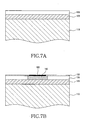
- FIG. 7a to 7e are sectional views showing a manufacturing process of a light receiving element according to a preferred embodiment of the present invention.
- an InP buffer layer (not shown), a photo-absorption layer 120, and a window layer 130 are formed in sequence, through a single crystal growth of the n-type InP substrate 110 using a Metal-Organic Chemical Vapor Deposition (MOCVD) process.
- the photo-absorption layer 120 is made of materials having smaller energy bandgap than that of wavelengths of light signals to be absorbed.
- InGaAs may be used to make the photo-absorption layer 120.
- the window layer 130 is made of materials having larger energy bandgap than that of wavelengths of light signals to be absorbed.
- InP may be used to make the window layer 130.
- a p-type InP active region 140 is formed by diffusing p-type impurities selectively in a predetermined region of the window layer 130, and passivation layer 150 is formed from dielectric materials so as to prevent oxidation of the interface of the window layer 130. Finally, a p-type electrode 160 is formed on the active region 140.
- a thinning process of grinding the InP substrate 110 to a desired thickness is performed, and etching masks 210 are selectively formed on one end of the InP substrate 110.
- a first groove area 220 and a second groove area 230 are determined by the etching masks 210, then the etching masks 210 is formed so that the first groove area 220 forms a portion of an edge of one side of the InP substrate 110.
- the etching masks 210 may be made of dielectric films such as SiN x , SiO 2 or PR (Photo Resist).
- the InP substrate 110 is etched using a wet etching process.
- An etching solution may be changed depending on the type of substrate.
- the wet etching makes use of the characteristic that (111) plane is etched more slowly than other directions in the crystal structure. Therefore, the wet etching is performed until the (111) plane appears.
- an InP substrate 110 is used, an HCl-based, an HBr-based or a Br-Me(OH)-based etching solution is used to form the (111) plane.
- (111) plane may be obtained by using a KOH-based etching solution if an Si substrate, or using a H 2 SO 4 -based etching solution of a GaAs substrate.
- an anti-reflective coating (ARC) layer 170 is formed on the first groove A using a Plasma Enhanced Chemical Vapor Deposition (PECVD) or a Sputter technique, forms N-metal 190 through sputtering or e-beam evaporation after opening N-type electrode region through photolithography process, and then a n-type electrode 190_Then, the anti-reflective coating layer 170 is deposited to a thickness and has a composition capable of achieving anti-reflective condition so that incident light is not reflected nor lost.
- PECVD Plasma Enhanced Chemical Vapor Deposition
- Sputter technique forms N-metal 190 through sputtering or e-beam evaporation after opening N-type electrode region through photolithography process, and then a n-type electrode 190_Then, the anti-reflective coating layer 170 is deposited to a thickness and has a composition capable of achieving anti-reflective condition so that incident light is not reflected nor lost.
- the light receiving element according to the present invention can improve a vertical-incidence angle of light signals toward the photo-absorption layer by 97° to 94° through refraction and reflection in the substrate. Therefore, loss of light can be minimized, and it has an effect in which process margin is greatly improved since vertical-incidence drift representing deviation degree of light signals according to thickness of substrates is very small.
- a light receiving element having vertical structure which cannot be constructed into a two-dimensional package in the prior art, can be constructed into a two-dimensional package. Therefore, in the work for optical coupling, the degree of freedom is reduced from three to two, and thus working error is reduced.
- an anti-reflective coating layer can be formed on a groove surface by using a simple PECVD process, so that it has an effect of increasing its process yield.
Applications Claiming Priority (2)
| Application Number | Priority Date | Filing Date | Title |
|---|---|---|---|
| KR10-2003-0019621A KR100464333B1 (ko) | 2003-03-28 | 2003-03-28 | 수광소자 및 그 제조방법 |
| KR2003019621 | 2003-03-28 |
Publications (2)
| Publication Number | Publication Date |
|---|---|
| EP1463123A2 true EP1463123A2 (de) | 2004-09-29 |
| EP1463123A3 EP1463123A3 (de) | 2010-11-03 |
Family
ID=32822764
Family Applications (1)
| Application Number | Title | Priority Date | Filing Date |
|---|---|---|---|
| EP04007552A Withdrawn EP1463123A3 (de) | 2003-03-28 | 2004-03-29 | Lichtempfindliches Element und sein Herstellungsverfahren |
Country Status (4)
| Country | Link |
|---|---|
| US (2) | US7161221B2 (de) |
| EP (1) | EP1463123A3 (de) |
| JP (1) | JP2004304187A (de) |
| KR (1) | KR100464333B1 (de) |
Families Citing this family (12)
| Publication number | Priority date | Publication date | Assignee | Title |
|---|---|---|---|---|
| JP5250165B2 (ja) * | 2005-02-23 | 2013-07-31 | ジョージア テック リサーチ コーポレーション | 端面視光検出器 |
| CN101730942A (zh) * | 2007-04-30 | 2010-06-09 | 陈小源 | 导波光伏装置 |
| JP2013058656A (ja) | 2011-09-09 | 2013-03-28 | Mitsubishi Electric Corp | 裏面入射型半導体受光素子 |
| JP6500442B2 (ja) * | 2014-02-28 | 2019-04-17 | 住友電気工業株式会社 | アレイ型受光素子 |
| JP6507891B2 (ja) * | 2015-07-03 | 2019-05-08 | 国立大学法人九州大学 | 導光部材、光導出部材及び光導出方法 |
| US10879415B2 (en) | 2017-06-23 | 2020-12-29 | Kabushiki Kaisha Toshiba | Photodetector, photodetection system, lidar apparatus, vehicle, and method of manufacturing photodetector |
| CN107516684A (zh) * | 2017-08-25 | 2017-12-26 | 深圳市芯思杰智慧传感技术有限公司 | 光电二极管芯片及其制作方法 |
| US20210083131A1 (en) * | 2017-08-31 | 2021-03-18 | Kyoto Semiconductor Co., Ltd. | End surface incident-type light receiving element |
| TW202010141A (zh) * | 2018-08-29 | 2020-03-01 | 鼎元光電科技股份有限公司 | 檢光二極體及其製造方法 |
| CN110880540A (zh) * | 2018-09-06 | 2020-03-13 | 鼎元光电科技股份有限公司 | 检光二极管及其制造方法 |
| US20210104638A1 (en) | 2019-10-04 | 2021-04-08 | Sensors Unlimited, Inc. | Visible-swir hyper spectral photodetectors with reduced dark current |
| US11355659B2 (en) * | 2019-11-27 | 2022-06-07 | Xintec Inc. | Chip package and manufacturing method thereof |
Citations (5)
| Publication number | Priority date | Publication date | Assignee | Title |
|---|---|---|---|---|
| EP0607524A1 (de) * | 1992-11-25 | 1994-07-27 | Robert Bosch Gmbh | Anordnung zur Ankopplung von Lichtwellenleiterenden an Sende- oder Empfangselemente |
| US5932114A (en) * | 1995-05-12 | 1999-08-03 | Fujitsu Limited | Integrated optical module including a waveguide and a photoreception device |
| US6049638A (en) * | 1997-05-22 | 2000-04-11 | Fujitsu Limited | Photodetector module |
| US6246097B1 (en) * | 1998-03-20 | 2001-06-12 | Oki Electric Industry Co., Ltd. | Semiconductor photodetector |
| US6353250B1 (en) * | 1997-11-07 | 2002-03-05 | Nippon Telegraph And Telephone Corporation | Semiconductor photo-detector, semiconductor photo-detection device, and production methods thereof |
Family Cites Families (8)
| Publication number | Priority date | Publication date | Assignee | Title |
|---|---|---|---|---|
| EP0397911A1 (de) * | 1989-05-19 | 1990-11-22 | Siemens Aktiengesellschaft | Optoelektronisches Halbleiterbauelement |
| JPH04336473A (ja) | 1991-05-14 | 1992-11-24 | Mitsubishi Electric Corp | 半導体受光装置 |
| DE19751650A1 (de) | 1997-11-21 | 1999-05-27 | Bosch Gmbh Robert | Optisches Bauelement |
| JPH11307806A (ja) * | 1998-04-17 | 1999-11-05 | Matsushita Electric Ind Co Ltd | 受光素子及びその製造方法 |
| JP2000261025A (ja) * | 1999-03-12 | 2000-09-22 | Toyoda Gosei Co Ltd | 受光素子 |
| JP4496636B2 (ja) | 2000-11-10 | 2010-07-07 | 株式会社デンソー | 光集積回路およびその製造方法 |
| JP3717785B2 (ja) * | 2000-12-28 | 2005-11-16 | ユーディナデバイス株式会社 | 半導体受光装置およびその製造方法 |
| JP2002344002A (ja) * | 2001-03-12 | 2002-11-29 | Matsushita Electric Ind Co Ltd | 受光素子及び受光素子実装体 |
-
2003
- 2003-03-28 KR KR10-2003-0019621A patent/KR100464333B1/ko not_active IP Right Cessation
- 2003-09-08 US US10/657,371 patent/US7161221B2/en not_active Expired - Fee Related
-
2004
- 2004-03-24 JP JP2004087467A patent/JP2004304187A/ja active Pending
- 2004-03-29 EP EP04007552A patent/EP1463123A3/de not_active Withdrawn
-
2005
- 2005-02-08 US US11/053,488 patent/US20050145965A1/en not_active Abandoned
Patent Citations (5)
| Publication number | Priority date | Publication date | Assignee | Title |
|---|---|---|---|---|
| EP0607524A1 (de) * | 1992-11-25 | 1994-07-27 | Robert Bosch Gmbh | Anordnung zur Ankopplung von Lichtwellenleiterenden an Sende- oder Empfangselemente |
| US5932114A (en) * | 1995-05-12 | 1999-08-03 | Fujitsu Limited | Integrated optical module including a waveguide and a photoreception device |
| US6049638A (en) * | 1997-05-22 | 2000-04-11 | Fujitsu Limited | Photodetector module |
| US6353250B1 (en) * | 1997-11-07 | 2002-03-05 | Nippon Telegraph And Telephone Corporation | Semiconductor photo-detector, semiconductor photo-detection device, and production methods thereof |
| US6246097B1 (en) * | 1998-03-20 | 2001-06-12 | Oki Electric Industry Co., Ltd. | Semiconductor photodetector |
Also Published As
| Publication number | Publication date |
|---|---|
| JP2004304187A (ja) | 2004-10-28 |
| US20050145965A1 (en) | 2005-07-07 |
| EP1463123A3 (de) | 2010-11-03 |
| KR100464333B1 (ko) | 2005-01-03 |
| US20040188787A1 (en) | 2004-09-30 |
| KR20040084495A (ko) | 2004-10-06 |
| US7161221B2 (en) | 2007-01-09 |
Similar Documents
| Publication | Publication Date | Title |
|---|---|---|
| US20050145965A1 (en) | Light receiving element and method of manufacturing the same | |
| US7148465B2 (en) | Semiconductor photodetector with internal reflector | |
| US20040241897A1 (en) | Edge-illuminated refracting-facet type light receiving device and method for manufacturing the same | |
| JP2002289904A (ja) | 半導体受光素子とその製造方法 | |
| US10218150B2 (en) | Wafer scale monolithic integration of lasers, modulators, and other optical components using ALD optical coatings | |
| JP2007013202A (ja) | 光検出器が集積可能な光結合装置 | |
| US6921956B2 (en) | Optical apparatus using vertical light receiving element | |
| KR20040015117A (ko) | 광자 집적회로 및 그 제조방법 | |
| JP3717785B2 (ja) | 半導体受光装置およびその製造方法 | |
| US6808957B1 (en) | Method for improving a high-speed edge-coupled photodetector | |
| US6395577B1 (en) | Photodetecting device and method of manufacturing the same | |
| JP2000150923A (ja) | 裏面入射型受光装置およびその作製方法 | |
| KR102307789B1 (ko) | 후면 입사형 애벌런치 포토다이오드 및 그 제조 방법 | |
| JP2001007353A (ja) | 光送受信モジュールおよびその製造方法 | |
| US20190109244A1 (en) | Semiconductor light receiving element and method for manufacturing the same | |
| JP3320058B2 (ja) | アングルキャビティ共鳴型光検出器組立体及びその製造方法 | |
| JP7409489B2 (ja) | 受光装置 | |
| KR100265858B1 (ko) | 반도체 레이저와 광검출기가 단일칩에 집적된 파장 분할 다중화 소자 | |
| JP2005093937A (ja) | 高速のエージ・カップル式フォトデテクタの改善方法 |
Legal Events
| Date | Code | Title | Description |
|---|---|---|---|
| PUAI | Public reference made under article 153(3) epc to a published international application that has entered the european phase |
Free format text: ORIGINAL CODE: 0009012 |
|
| 17P | Request for examination filed |
Effective date: 20040329 |
|
| AK | Designated contracting states |
Kind code of ref document: A2 Designated state(s): AT BE BG CH CY CZ DE DK EE ES FI FR GB GR HU IE IT LI LU MC NL PL PT RO SE SI SK TR |
|
| AX | Request for extension of the european patent |
Extension state: AL LT LV MK |
|
| PUAL | Search report despatched |
Free format text: ORIGINAL CODE: 0009013 |
|
| AK | Designated contracting states |
Kind code of ref document: A3 Designated state(s): AT BE BG CH CY CZ DE DK EE ES FI FR GB GR HU IE IT LI LU MC NL PL PT RO SE SI SK TR |
|
| AX | Request for extension of the european patent |
Extension state: AL LT LV MK |
|
| AKX | Designation fees paid |
Designated state(s): DE FR GB |
|
| 17Q | First examination report despatched |
Effective date: 20110704 |
|
| RAP1 | Party data changed (applicant data changed or rights of an application transferred) |
Owner name: SAMSUNG ELECTRONICS CO., LTD. |
|
| STAA | Information on the status of an ep patent application or granted ep patent |
Free format text: STATUS: THE APPLICATION IS DEEMED TO BE WITHDRAWN |
|
| 18D | Application deemed to be withdrawn |
Effective date: 20160719 |