EP1455986B1 - Method of laser machining a fluid slot - Google Patents
Method of laser machining a fluid slot Download PDFInfo
- Publication number
- EP1455986B1 EP1455986B1 EP02747939A EP02747939A EP1455986B1 EP 1455986 B1 EP1455986 B1 EP 1455986B1 EP 02747939 A EP02747939 A EP 02747939A EP 02747939 A EP02747939 A EP 02747939A EP 1455986 B1 EP1455986 B1 EP 1455986B1
- Authority
- EP
- European Patent Office
- Prior art keywords
- slot
- substrate
- laser
- laser beam
- illustrates
- Prior art date
- Legal status (The legal status is an assumption and is not a legal conclusion. Google has not performed a legal analysis and makes no representation as to the accuracy of the status listed.)
- Expired - Lifetime
Links
Images


Classifications
-
- B—PERFORMING OPERATIONS; TRANSPORTING
- B23—MACHINE TOOLS; METAL-WORKING NOT OTHERWISE PROVIDED FOR
- B23K—SOLDERING OR UNSOLDERING; WELDING; CLADDING OR PLATING BY SOLDERING OR WELDING; CUTTING BY APPLYING HEAT LOCALLY, e.g. FLAME CUTTING; WORKING BY LASER BEAM
- B23K26/00—Working by laser beam, e.g. welding, cutting or boring
- B23K26/02—Positioning or observing the workpiece, e.g. with respect to the point of impact; Aligning, aiming or focusing the laser beam
- B23K26/06—Shaping the laser beam, e.g. by masks or multi-focusing
- B23K26/067—Dividing the beam into multiple beams, e.g. multi-focusing
- B23K26/0676—Dividing the beam into multiple beams, e.g. multi-focusing into dependently operating sub-beams, e.g. an array of spots with fixed spatial relationship or for performing simultaneously identical operations
-
- B—PERFORMING OPERATIONS; TRANSPORTING
- B23—MACHINE TOOLS; METAL-WORKING NOT OTHERWISE PROVIDED FOR
- B23K—SOLDERING OR UNSOLDERING; WELDING; CLADDING OR PLATING BY SOLDERING OR WELDING; CUTTING BY APPLYING HEAT LOCALLY, e.g. FLAME CUTTING; WORKING BY LASER BEAM
- B23K26/00—Working by laser beam, e.g. welding, cutting or boring
- B23K26/16—Removal of by-products, e.g. particles or vapours produced during treatment of a workpiece
-
- B—PERFORMING OPERATIONS; TRANSPORTING
- B23—MACHINE TOOLS; METAL-WORKING NOT OTHERWISE PROVIDED FOR
- B23K—SOLDERING OR UNSOLDERING; WELDING; CLADDING OR PLATING BY SOLDERING OR WELDING; CUTTING BY APPLYING HEAT LOCALLY, e.g. FLAME CUTTING; WORKING BY LASER BEAM
- B23K26/00—Working by laser beam, e.g. welding, cutting or boring
- B23K26/36—Removing material
- B23K26/38—Removing material by boring or cutting
- B23K26/382—Removing material by boring or cutting by boring
- B23K26/384—Removing material by boring or cutting by boring of specially shaped holes
-
- B—PERFORMING OPERATIONS; TRANSPORTING
- B23—MACHINE TOOLS; METAL-WORKING NOT OTHERWISE PROVIDED FOR
- B23K—SOLDERING OR UNSOLDERING; WELDING; CLADDING OR PLATING BY SOLDERING OR WELDING; CUTTING BY APPLYING HEAT LOCALLY, e.g. FLAME CUTTING; WORKING BY LASER BEAM
- B23K26/00—Working by laser beam, e.g. welding, cutting or boring
- B23K26/36—Removing material
- B23K26/38—Removing material by boring or cutting
- B23K26/382—Removing material by boring or cutting by boring
- B23K26/389—Removing material by boring or cutting by boring of fluid openings, e.g. nozzles, jets
-
- B—PERFORMING OPERATIONS; TRANSPORTING
- B41—PRINTING; LINING MACHINES; TYPEWRITERS; STAMPS
- B41J—TYPEWRITERS; SELECTIVE PRINTING MECHANISMS, i.e. MECHANISMS PRINTING OTHERWISE THAN FROM A FORME; CORRECTION OF TYPOGRAPHICAL ERRORS
- B41J2/00—Typewriters or selective printing mechanisms characterised by the printing or marking process for which they are designed
- B41J2/005—Typewriters or selective printing mechanisms characterised by the printing or marking process for which they are designed characterised by bringing liquid or particles selectively into contact with a printing material
- B41J2/01—Ink jet
- B41J2/135—Nozzles
- B41J2/16—Production of nozzles
- B41J2/1601—Production of bubble jet print heads
- B41J2/1603—Production of bubble jet print heads of the front shooter type
-
- B—PERFORMING OPERATIONS; TRANSPORTING
- B41—PRINTING; LINING MACHINES; TYPEWRITERS; STAMPS
- B41J—TYPEWRITERS; SELECTIVE PRINTING MECHANISMS, i.e. MECHANISMS PRINTING OTHERWISE THAN FROM A FORME; CORRECTION OF TYPOGRAPHICAL ERRORS
- B41J2/00—Typewriters or selective printing mechanisms characterised by the printing or marking process for which they are designed
- B41J2/005—Typewriters or selective printing mechanisms characterised by the printing or marking process for which they are designed characterised by bringing liquid or particles selectively into contact with a printing material
- B41J2/01—Ink jet
- B41J2/135—Nozzles
- B41J2/16—Production of nozzles
- B41J2/1607—Production of print heads with piezoelectric elements
-
- B—PERFORMING OPERATIONS; TRANSPORTING
- B41—PRINTING; LINING MACHINES; TYPEWRITERS; STAMPS
- B41J—TYPEWRITERS; SELECTIVE PRINTING MECHANISMS, i.e. MECHANISMS PRINTING OTHERWISE THAN FROM A FORME; CORRECTION OF TYPOGRAPHICAL ERRORS
- B41J2/00—Typewriters or selective printing mechanisms characterised by the printing or marking process for which they are designed
- B41J2/005—Typewriters or selective printing mechanisms characterised by the printing or marking process for which they are designed characterised by bringing liquid or particles selectively into contact with a printing material
- B41J2/01—Ink jet
- B41J2/135—Nozzles
- B41J2/16—Production of nozzles
- B41J2/1621—Manufacturing processes
- B41J2/1632—Manufacturing processes machining
- B41J2/1634—Manufacturing processes machining laser machining
Definitions
- the present invention relates to a method of laser machining a fluid channel according to preamble of claim 1.
- JP-06-079486 A discloses in combination all features of preamble of claim 1.
- thermal actuated printheads tend to use resistive elements or the like to achieve ink expulsion
- mechanically actuated printheads tend to use piezoelectric transducers or the like.
- a representative thermal inkjet printhead has a plurality of thin film resistors provided on a semiconductor substrate.
- An orifice and/or a barrier layer is provided on the substrate.
- the orifice and/or the barrier layer defines firing chambers about each of the resistors, an orifice corresponding to each resistor, and an entrance to each firing chamber. Actuation of a heater resistor by a "fire signal" causes ink in the corresponding firing chamber to be heated and expelled through the corresponding orifice.
- Ink typically is provided at the entrance of the firing chamber through a feed slot that is machined in the semiconductor substrate.
- the substrate usually has a rectangular shape, with the slot disposed longitudinally therein.
- Resistors are often arranged in rows located on one or both sides of the slot. The width of the print swath achieved by one pass of a printhead is approximately equal to the length of the resistor rows, which in turn is approximately equal to the length of the slot.
- Feed slots have typically been formed by sand drilling (also known as sandblasting or "sand slotting").
- sand blasting also known as sandblasting or "sand slotting”
- This method is a rapid, relatively simple and scalable process.
- the sand blasting method is capable of forming an opening in a substrate with a relatively high degree of accuracy for simple slot shapes, while generally avoiding substantial damage to surrounding components and materials. Also, it is capable of cutting openings in various substrates having different materials without the generation of excessive heat. Furthermore, it allows for improved relative placement accuracies during the production process.
- sand slotting affords these apparent benefits, sand slotting is also disadvantageous in that it may cause microcracks in the semiconductor substrate that significantly reduce the substrate's fracture strength, resulting in significant yield loss due to cracked die. Low fracture strength also limits substrate length which in turn adversely impacts print swath height and overall print speed.
- sand slotting typically causes chips to the substrate on both the input and output side of the slot. Normally the chipping is tens of microns large and limits how close the firing chamber can be placed to the edge of the slot. Occasionally the chipping is larger and causes yield loss in the manufacturing process. The chipping problem is more prevalent as the desired slot length increases and the desired slot width decreases.
- Feed slots may also be formed by wet chemical etching with, for example, alkaline etchants. Such etching techniques result in etch angles that cause a very wide backside slot opening.
- the wide backside opening limits how small a particular die on the wafer could be and therefore limits the number of die per wafer (the separation ratio). It is desired to maximize the separation ratio.
- the invention consists in a method of laser machining a fluid channel according to claim 1.
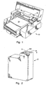
- Fig. 1 is a perspective view of a printer 10 for printing on media 22 with a print cartridge (or ejection cartridge) 12.
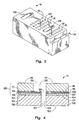
- Fig. 2 is a perspective view of the cartridge 12 with a printhead (or fluid drop generator or fluid ejection device) 14 of an embodiment of the present invention. Fluid or ink is ejected or fired out from nozzles 132 to the media 22.
- Fig. 3 illustrates an enlarged view of one embodiment of the printhead 14 in perspective view.
- the printhead 14 in this embodiment has multiple features, including an edge step 119 for an edge fluid feed to resistors (or fluid ejectors) 61.
- the printhead also has a trench 124 that is partially formed into the substrate surface.
- a slot (or channel) 126 for a slot fluid feed to resistors 61, and/or a series of holes 127 feeding fluid to resistors 61 are also shown on this printhead, each being formed by a UV laser machining process as described herein.
- the trench 124 may also be formed by the UV laser machining processes as described further below.
- the edge step and/or the trench 124 are formed as well.
- the edge step 119, and the slot 126 are formed in the printhead 14, where in an alternative embodiment the trench 124 and/or the feedholes 127 are formed as well.
- Fig. 4 illustrates a cross-sectional view of the printhead 14 of Fig. 2 where the slot 126 having slot (or side) walls 123 is formed through a substrate 102.
- the formation of the slot through a slot region (or slot area) in the substrate is described in more detail below.
- a higher density of slots is etched in a given die.
- the inter slot spacing or spacing between adjacent slots in the die or substrate are as low as 10 microns. (In an embodiment, 10 microns is just over twice the extent of a heat affected zone for each slot, where the heat affected zone is the area along the slot walls that is affected by the laser machining described in this application.)
- a thin film layer (or an active layer, a thin film stack, an electrically conductive layer, or a layer with micro-electronics) 120 that is formed or deposited on a front or first side (or surface) 121 of the substrate 102 is illustrated.
- the first side 121 of the substrate is opposite a second side (or surface) 122 of the substrate 102.
- the thin film stack 120 is at least one layer formed on the substrate, and, in a particular embodiment, masks at least a portion of the first side 121 of the substrate 102.
- the layer. 120 electrically insulates at least a portion of the first side 121 of the substrate 102.
- the thin film stack 120 includes a capping layer 104, a resistive layer 107, a conductive layer 108, a passivation layer 110, a cavitation barrier layer 111, and a barrier layer 112, each formed or deposited over the first side 121 of the substrate 102 and/or the previous layer(s).
- the substrate 102 is silicon.
- the substrate is one of the following: single crystalline silicon, polycrystalline silicon, gallium arsenide, glass, silica, ceramics, or a semiconducting material.
- the various materials listed as possible substrate materials are not necessarily interchangeable and are selected depending upon the application for which they are to be used.
- the thin film layers are patterned and etched, as appropriate, to form the resistors 61 in the resistive layer, conductive traces of the conductive layer, and a firing chamber 130 at least in part defined by the barrier layer.
- the barrier layer 112 defines the firing chamber 130 where fluid is heated by the corresponding resistor and defines a nozzle orifice 132 through which the heated fluid is ejected.
- an orifice layer (not shown) having the orifices 132 is applied over the barrier layer 112.
- An example of the physical arrangement of the barrier layer, and thin film substructure is illustrated at page 44 of the Hewlett-Packard Journal of February 1994. Further examples of ink jet printheads are set forth in commonly assigned U.S. Pat.
- At least one layer or thin film layer is formed or deposited upon the substrate 102.
- Embodiments of the present invention include having any number and type of layers formed or deposited over the substrate (or no layers at all), depending upon the application for which the slotted substrate is to be utilized.
- a channel 129 is formed as a hole or fluid feed slot 129 through the layers (120) formed upon the substrate.
- the channel 129 fluidically couples the firing chamber 130 and the slot 126, such that fluid flows through the slot 126 and into the firing chamber 130 via channel 129.
- the channel entrance 129 for the fluid is not in the center of the slot 126.
- the slotted substrate is formed as described below substantially the same in either instance where the entrance 129 is centrally located or off-center.
- a plan and a perspective view of the printhead 14 and its slot 126 is shown without the barrier layer 112 (for Fig. 4A) and without the stack 120 (for Fig. 4B).
- the resistors 61 are along the slot 126.
- the slot wall 123 has striations (or vertical lines) 142, and a rough area (or breakthrough area) 144 near the middle of the slot 126 formed by the slotting process of the present invention.
- the rough area 144 is formed by a breakthrough near the middle of the slot 126.
- slots formed by an embodiment of the present invention have chip sizes along the surfaces of the substrate of at most 3 microns, if any.
- the slot 126 has a wall edge 146.
- the roughness (or smoothness) of the wall edge 146 along the front side 121 of the substrate is about 3 microns, and about 5 microns along the second side 122 of the substrate, although in the embodiment the roughness could be more or less.
- the thin film layer or stack 120 is formed, masked and patterned over the first side 121 of the wafer or substrate 102 to form the recess 129, as shown in Fig. 6A.
- a hard mask and/or a photoimagable material layer are additionally formed on the backside 122 of the substrate opposite the thin film layer 120.
- the slot formation is begun using a UV laser beam 140 (See Fig. 6A) directed to an area of the substrate to be slotted.
- an area on the second side 122 of the substrate is the initial area to be exposed to the UV laser beam.
- the substrate material in the area of the substrate that is exposed to the UV laser beam is ablated and/or vaporized to form the slot, 126, as described in more detail below.
- debris or residue 149 from the laser machining begins to form along the slot walls 123 as well as along the bottom of the trench being formed in the substrate.
- the debris may be formed of polycrystalline and/or amorphous silicon oxide.
- the substrate 102 is laser machined to a depth x.
- the laser beam 140 is directed towards the first side or surface 121 of the substrate through the recess in the thin film stack 120, as shown in Fig. 6B.
- y is about 20 microns.
- x is about twice y.
- x is about the same as y.
- y is greater than x.
- steps 210 and 220 are repeated for each slot 126 in the die (or substrate).
- throughput is improved with the described bi-directional process because the debris (or redeposited material) 149 escapes the machined channel more readily in shallower rather than deeper trenches.
- the majority of the debris that escapes the machined channels escapes from the backside 122, thereby limiting the amount of contamination to the active layer(s) 120 on the front side 121 of the substrate.
- the UV laser etch is performed first from the first side 121, and then from the second side 122 to meet at the breakthrough area 144.
- the laser machining is provided by a UV laser beam 140 (Fig. 6A), and in one particular embodiment, is provided by a diode-pumped solid-state pulsed UV laser.
- the UV laser 140 originates from a Xise 200 Laser Machining Tool, manufactured by Xsil of Dublin, Ireland.
- a laser source 139 (shown in Figs. 9A and 9B) uses power in the range of about 2 to 100 Watts, and more particularly about 4.5 Watts.
- the UV wavelength is less than about 400 nm, in particular about 355 nm.
- the pulse width of the laser beam is about 15 ns in this embodiment, and the repetition rate is about 30 kHz.
- the laser beam has a diameter of about 5 to 100 microns, and more particularly about 30 microns in this embodiment.
- the laser-machining tool of the present invention has a debris extraction system to remove the debris 149 resulting from the laser machining.
- the intense UV light is absorbed into less than about 1 micron of the surface of the material being ablated. Because the light energy is so concentrated near the surface of the material, the material rapidly heats, melts, and vaporizes. A mixture of vapor and molten droplets are then quickly ejected away. Consequently, the surrounding region (or heat affected zone) is not melted substantially or otherwise substantially damaged because the process happens so quickly, and there is not enough time for significant heat to propagate to the surrounding regions.
- a more in depth explanation of the process is described on pps. 131-134 of Laser-Beam Interactions with Materials: Physical Principles and Applications , 2nd updated edition, 1995, written by Martin von Allmen & Andreas Blatter.
- slots formed by embodiments of the present invention again have surface roughness of at most 5 microns.
- the rough area 144 near the center of the slot is redeposited material caused by heated fragments that were not efficiently extracted due to the depth of the trench. These fragments subsequently melted and resolidified to form the debris 149.
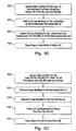
- step 300 is similar to step 200 of Fig. 5A.
- Steps 310 and 320 can be considered similar to steps 210 and 220 of Fig. 5A, however, some differences are as follows.
- First in step 310 each slot on the die is partially formed from the second side 122. Then each partially formed slot is completed when the laser beam is directed towards the first side 121 in step 320. In other words, no repetition of previous steps occurs in this embodiment.
- a beam splitter is used to partially form slots from the second side in step 310 and/or is used to complete slotting from the first side in step 320, wherein the beam splitter is discussed in more detail below with regard to Figs. 8A and 8B.
- the first side 121 is subjected to the laser machining process before the second side 122 thereby reversing steps 310 and 320.
- step 400 is similar to step 200 of Fig. 5A.
- step 410 two or more slots on the die or wafer are partially formed simultaneously from the second side 122 of the die.
- step 420 those two or more slots 126 are fully formed simultaneously from the front side 121.
- steps 410 and 420 are repeated until each of the slots are formed in step 430.
- two or more slots are formed in step 420, or partially formed in step 410, simultaneously through use of the beam splitters discussed below.
- the first side 121 is subjected to the laser machining process before the second side 122 thereby reversing the steps 410 and 420.
- Figs. 5B and 5C can be combined such that two or more slots are partially formed simultaneously from the second side 122. Then, each slot on the die is partially formed from the second side (in groups of two or more slots simultaneously) before any of the slots are fully formed by laser machining from the front side of the die (in groups of two or more slots simultaneously).
- the first side 121 is subjected to the laser machining process before the second side 122.
- steps 500, 510 and 520 are similar to steps 200, 210 and 220 of Fig. 5A, with some differences as follows.
- the slot is laser-machined from the second side in step 510, and then laser-machined from the first side of the substrate in step 520. After the slot is laser-machined from both sides, the slot is still not yet fully formed in that the laser machining has not fully broken through the substrate 102, as opposed to be completely formed after step 220.
- the partially formed slot is laser machined from the second side again, until breakthrough occurs.
- steps 510 to 530 are repeated for each slot on the die.
- step 510 is performed for each partially formed slot on the second side, then step 520 is performed for each partially formed slot on the first side, and then step 530 is performed for each partially formed slot on the second side until breakthrough occurs.
- the first side is partially laser machined, then the second side is partially laser machined, and then ultimate breakthrough occurs from the first side.
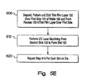
- steps 600 and 610 are similar to step 200 and 210 with some differences as follows.
- the laser machining from the second side breaks all the way through to the first surface of the substrate.
- the step 610 is repeated for each slot 126 to be formed in the die.
- the barrier layer 112 is formed with the thin film stack 120 over the first side 121 of the substrate in step 600.
- step 600 is performed after step 620 is completed.
- the UV laser machining of the slot is fully performed from the first side 121 of the substrate.
- Figs. 6E to 6L illustrate various embodiments of a slot profile in a substrate 102.
- the slot profile is not to scale. Generally, the slot profile is narrower than as depicted.
- the slot profiles are depicted in these drawings as wider than in general for ease of viewing the distinctions in the slot profiles.
- the substrate 102 is illustrated in these embodiments as having active layer (or layer with microelectronics) 120 on a first side of the substrate. However, in alternative embodiments, the active layer(s) 120 is on the second side of the substrate.
- the slot profile is formed by one of the laser machining process described above, including a bi-directional laser machining process.
- Fig. 6E illustrates an embodiment of the slotted substrate 102 having stepped slot walls 128.
- the slot walls 128 of Fig. 6E have varying cross-sectional areas that incrementally decrease from the second surface 122 to the first surface 121.
- the slot width a is adjacent the first surface 121
- the slot width c is adjacent the second surface 122
- the slot width b is in between a and c.
- the slot width a is 210 microns
- the slot width b is 220 microns
- the slot width c is 260 microns.
- the slot width near the first surface is in a range of about 5 to 100 microns
- the slot width near the second surface is in a range of about 100 to 300 microns, where the slot width near the second surface is greater than that of the first surface.
- the width near the second surface is at least 10% greater than that of the first surface.
- the slot width near the second surface is about 140 microns
- the slot width near the first surface is about 50 microns.
- the slot profile is formed as follows: the slot widths b and c are formed from the second side 122, then the slot width a is formed from the first side 121. In another embodiment, each of the slot widths are consecutively formed from the second side 122. In a first embodiment, the slot width a is formed, then slot width b, then slot width c. In a second embodiment, the slot width c is formed, then slot width b, then slot width a. However, various other embodiments are envisioned, including forming slot width b, then slot width c, then slot width a, especially when using bi-directional laser machining processes.
- Fig. 7E illustrates an embodiment where laser beams are traced in a multiple cookie-cutter pattern 156 to form the slot 126.
- the laser beams traced are substantially concentric elliptical shapes: shapes m, n, and p, where shape m is the smallest elliptical shape, and shape p is the largest elliptical shape as shown in Fig. 7E.
- shape m is the smallest elliptical shape
- shape p is the largest elliptical shape as shown in Fig. 7E.
- the shapes n and p are traced first, then the shape m is traced, where the shape m corresponds to the slot width a, the shape n corresponds to the slot width b, and the shape p corresponds to the slot width c.
- Other orders of tracing are envisioned with alternate embodiments of this invention. Additional embodiments of laser beam tracing patterns are illustrated in and described with respect to Figs. 7A to 7F.
- Fig. 6F illustrates an embodiment of the slotted substrate 102 having substantially tapered and smoothed slot walls 125.
- the slot walls 125 of Fig. 6F have varying cross-sectional areas and incrementally decrease from the second surface 122 to the first surface 121.
- the slot profile approaches the first surface 121, the slot profile narrows and then expands slightly to the first surface 121. Because the slot profile narrows and expands near the first surface in this embodiment, there is a non-symmetrical hourglass shape with respect to the first and second surfaces of the substrate.
- the slot width adjacent the first surface is labeled as a.
- the slot width adjacent the second surface is labeled as c.
- the slot widths a and c of Fig. 6F are similar to the slot widths of Fig. 6E.
- the slot walls 125 are formed by the method described with respect to Figs. 6A and 6B.
- the breakthrough area of the slot has the narrower cross-sectional area as described above and shown in Fig. 6F.
- the slot walls 125 of Fig. 6F are formed by first forming the slot profile shown in Fig. 6E. In this embodiment, the stepped slot walls 128 are then smoothed out to form the tapered walls 125 of Fig. 6F. Methods of smoothing are discussed in more detail below. In an alternative embodiment, the smoothed out walls have a slight curvature. In another embodiment, the slot profile tapers from the second surface 122 to the first surface 121 without the narrow cross-sectional area in the slot profile.
- Fig. 6G illustrates an embodiment of the slot profile having a substantially hourglass-type shape, where the narrowing section 144 near the middle is formed when the breakthrough in the silicon occurs.
- the slot has tapered walls 125 that taper towards the middle of the slot from both the first and second surfaces of the substrate 102.
- This embodiment is generally formed with the bi-directional fluid slot formation described above with respect to flow chart Fig. 5A.
- Fig. 6H illustrates an embodiment of the slot profile having substantially straight slot walls. These slot walls are formed using the smoothing methods described below. In one embodiment, these walls are formed by one of the methods described above.
- Fig. 61 illustrates an embodiment of the slot profile having a compound slot shape.
- Fig. 61 illustrates a slot profile having an hourglass-type shape with a counterbore in the second surface.
- the embodiment of the slot profile of Fig. 61 has wall surfaces 125 tapering from each substrate surface, as well as wall surfaces 128 that are stepped, i.e. orthogonal to the direction of the laser beam, forming the counterbore. In one embodiment, these walls 125 and 128 are formed by at least one of the methods described herein.
- Fig. 6J illustrates another embodiment of the slot profile having a compound slot shape.
- Fig. 6J illustrates a slot profile with a counterbore having a stepped wall 128.
- Fig. 6J is similar to the embodiment described with respect to Fig. 6E, except Fig. 6J has only one step in the slot profile.
- the methods for forming Fig. 6E and other methods for forming slot walls described herein apply, as appropriate, to this current embodiment shown in Fig. 6J.
- Fig. 6K illustrates an embodiment of the slot profile having a compound slot shape.
- Fig. 6K illustrates a slot profile having an hourglass-type shape with an offset counterbore.
- the embodiment of the slot profile of Fig. 6K has one slot wall with tapered surfaces 125 as shown and described with respect to Fig. 6G, as well as one slot wall with a stepped surface 128 and a tapered surface 125 as shown and described with respect to Fig. 61. In one embodiment, these walls are formed by at least one of the methods described herein.
- Fig. 6L illustrates another embodiment of the slot profile having a compound slot shape.
- Fig. 6L illustrates a slot profile with offset counterbores having stepped walls 128.
- the stepped walls on each side of the slot shift over in the same direction such that the cross-sectional area at substantially all points along the slot profile remains substantially the same.
- these walls are formed by at least one of the methods described herein.
- Figs. 7A to 7F illustrate various embodiments of laser beam patterns, including laser beam trace spacing.
- the laser beams are directed toward a slot area on either (or both) the first surface 121 and the second surface 122 in forming the slotted substrates of the present invention.
- the applied laser beam patterns determine the slot areas, and thus, the slot shapes on the substrate surfaces.
- a laser beam pattern is repeatedly applied to the substrate in forming the fluid feature.
- multiple laser beam patterns are applied to the substrate in forming the fluid feature.
- the slot area on each side/surface of the substrate is about 260 microns x 8480 microns.
- the slot area on the first surface is about 210 microns x 8480 microns, and about 260 microns x 8480 microns on the second surface.
- the slot widths are as narrow as 5 to 10 microns, and as wide as 300 microns.
- the slot widths are 30-50 microns or 80 microns, depending upon the application of the fluid slot.
- having a low aspect ratio increases the laser machining speed, due to debris interference associated with high aspect ratio features.
- debris accumulation along the slot walls is much greater than slot widths of greater than about 80 microns.
- Fig. 7A illustrates an embodiment where laser beams are traced in a raster or serpentine pattern 150 to form the slot 126 in the printhead 14.
- the laser beams are traced starting at one end of the slot area, then traced back and forth in the longitudinal direction until reaching the opposite longitudinal end of the slot.
- the spacing between adjacent laser beam traces is substantially constant.
- Fig. 7B illustrates an embodiment where laser beams are traced in a substantially spiral pattern 152 to form the slot 126.
- the laser beams are traced starting at the center of the slot and move in a circular pattern gradually increasing in size to form the slot 126 shape.
- the laser beams are traced starting along the edges of the desired slot shape and gradually decreasing in size while moving in a substantially circular pattern.
- Fig. 7C illustrates an embodiment where laser beams are traced in a cookie cutter pattern 154 to form the slot 126.
- the laser beams are traced along the edges of the desired slot shape of the slot 126.
- Fig. 7D illustrates an embodiment where laser beams are traced in a cookie cutter pattern 154, as described and shown with respect to Fig. 7C, as well as the raster pattern 150, as described and shown with respect to Fig. 7A, to form the slot 126. Either pattern 150 or 154 is traced first.
- Fig. 7E for forming a slot using the multiple cookie-cutter laser beam pattern 156 has previously been described.
- there are a plurality of traces in the cookie-cutter laser beam pattern such as two traces, or as many as practically possible.
- the laser beam traces become successively smaller (or larger), and successive laser beams are directed to a lower (or higher) depth in the substrate.
- the slot walls increasingly become smoother.
- Fig. 7F illustrates an embodiment where laser beams are traced in a modified window pattern 158 to form the slot 126.
- the laser beam is traced in a closed loop within the edges of the desired slot shape of the slot 126.
- each consecutive laser beam trace is larger than the previous closed loop.
- each consecutive laser beam trace is smaller than the previous closed loop.
- the spacing between consecutive traces is maintained substantially constant except near the end of the slot.
- the closed loop of each consecutive laser beam trace overlaps on each slot end. In this embodiment, there are 4 closed loops overlapping at each slot end. In alternative embodiments, there are at least 2 closed loops.
- slot profiles that combine steps, tapered walls, smooth walls, and counterbores are envisioned with the present invention.
- the stepped, tapered, smooth or otherwise varied slot walls of the embodiments shown in Figs. 6A through 6L are formed by varying the laser process, trace, or laser beam source.
- varying the laser beam or the laser process include varying the laser beam diameter by moving the laser beam focus in a z-direction (towards or away from the substrate), and adjusting the UV laser machine.
- the laser beam diameter may be varied using a beam expander.
- the beam expander is Galilean, where there is no internal focus that can lead to air break down with high energy pulsed lasers.
- Keplerian telescopes are used at lower energies.
- a scan speed, a pulse width, a repetition rate, focusing lens, laser power, etc. may be adjusted on the UV laser machine to vary the laser beam or laser process.
- the laser power may be reduced at or near surface breakthrough to minimize damage, including chipping and cracking, to the substrate surface (especially for reducing damage to slot edges in the surface with active layers).
- the laser beam is defocused in order to clean the slot and the substrate.
- Figs. 8A to 8B illustrate various embodiments of optical schemes for splitting the laser beam 140.
- the laser beam 140 comes from the laser source 139.
- the high-energy pulse laser beam 140 is split into a number of beamlets such that the energy of each beamlet has optimum energy, and hence optimum etch depth.
- increases in laser power are used to produce two beams with more optimal conditions.
- Fig. 8A illustrates splitting the beam using conventional optics
- Fig. 8B illustrates an alternative embodiment of splitting the beam using diffractive optics.
- embodiments of the present invention are applicable to beams of any size. In other embodiments, more than two beams or beamlets having the optimum energy are envisioned with the present invention.
- Fig. 8A illustrates the embodiment where the laser beam 140 hits a 50/50 beam splitter 180, where the beam splits into two beamlets.
- a first one of the beamlets continues in the same direction and, upon reaching a first focusing lens 184, is focused to the printhead 14 (or substrate) for laser machining the substrate.
- a second one of the beamlets is deflected in a perpendicular direction and the beamlet subsequently hits a mirror 182 and is deflected towards a second focusing lens 184 to be focused to the printhead (or substrate) adjacent the first of the beamlets.
- two laser beams are able to machine two slots on a substrate simultaneously.
- Fig. 8B illustrates splitting the beam using diffractive optics.
- Fig. 8B illustrates the embodiment where the laser beam 140 hits a diffractive element 186, where the beam splits into two beamlets. Each of the two beamlets continues in substantially the same direction towards the substrate to a focusing lens 184. The laser beamlets are then focused to slot areas or areas to be laser machined on the substrate or printhead 14. In this alternative manner, two laser beams are able to machine two slots or two areas on a substrate simultaneously.
- Figs. 9A to 9B illustrate one embodiment of steps to move the laser beam focal point in the z-direction.
- the laser source 139 of the laser beam 140 is moved from a first position relative to the substrate 102, shown in Fig. 9A, to a closer position relative to the substrate 102, shown in Fig. 9B.
- the distance between the laser source and the substrate being etched increases. Consequently, in the embodiment shown, the focus of the laser beam is altered non-optimally (due to beam attenuation) and/or the amount of debris 149 increases.
- the laser beam focal point is adjusted with the increasing depth.
- Figs. 10A to 10B illustrate embodiments depicting laser beam power or intensity over a laser beam cross-section and the profile of the subsequently ablated material.
- Fig. 10A is an embodiment depicting a laser beam 700 with a Gaussian distribution of laser intensity.
- a Gaussian laser power or intensity curve 701 over the beam cross-section is shown.
- the laser beam 700 contacts a surface 702 of the material substantially within the area marked by the dashed lines.
- the laser beam 700 renders the ablated material with a curved surface 702.
- a central area 704 of the material is ablated to a larger degree than edge or periphery areas, due to the greater intensity of the laser beam in the center.
- the curved surface 702 may not be optimum due to the uneven topology.
- Fig. 10B illustrates an embodiment of a laser beam having uniform intensity for the laser beam power, or 'top hat' laser beams 800.
- a uniform laser power or intensity curve 801 over the beam cross-section is shown.
- the laser beam 800 contacts the surface 802 substantially within the dashed lines in Fig. 10B at surface 804. Even though the laser beam is not purposefully directed towards areas adjacent to surface 804, also known as edge or periphery areas 806, these areas 806 are affected in some embodiments.
- the laser beam 800 renders the ablated material with a substantially flat surface 804 in the area that the laser beam 800 directly contacts, and a curved surface along the periphery 806.
- the area 804 is substantially uniformly ablated, i.e. flat.
- the uniform intensity beam is achieved using (a) a beam expanding telescope, mask and imaging lens, (b) Diffractive Optical Elements and/or (c) beam homogeniser units (such as segmented mirrors).
- the present invention is not limited to thermally actuated printheads, but may also include, for example, piezoelectric activated printheads, and other mechanically actuated printheads, as well as other applications having micro-fluidic channels through a substrate.
- Methods of forming micro-fluidic channels described above may also be applied to micro-electromechanical, systems (MEMS) that include atomic resolution storage devices, fuel cells, sensors, and displays, for example.
- MEMS micro-electromechanical, systems
Landscapes
- Engineering & Computer Science (AREA)
- Physics & Mathematics (AREA)
- Optics & Photonics (AREA)
- Plasma & Fusion (AREA)
- Mechanical Engineering (AREA)
- Manufacturing & Machinery (AREA)
- Particle Formation And Scattering Control In Inkjet Printers (AREA)
- Laser Beam Processing (AREA)
Priority Applications (1)
| Application Number | Priority Date | Filing Date | Title |
|---|---|---|---|
| EP06076894A EP1769872A3 (en) | 2001-12-20 | 2002-06-21 | Method of laser machining a fluid slot |
Applications Claiming Priority (5)
| Application Number | Priority Date | Filing Date | Title |
|---|---|---|---|
| US138594 | 1998-08-22 | ||
| US34347601P | 2001-12-20 | 2001-12-20 | |
| US343476P | 2001-12-20 | ||
| US10/138,594 US7357486B2 (en) | 2001-12-20 | 2002-05-02 | Method of laser machining a fluid slot |
| PCT/US2002/019752 WO2003053627A1 (en) | 2001-12-20 | 2002-06-21 | Method of laser machining a fluid slot |
Related Child Applications (1)
| Application Number | Title | Priority Date | Filing Date |
|---|---|---|---|
| EP06076894A Division EP1769872A3 (en) | 2001-12-20 | 2002-06-21 | Method of laser machining a fluid slot |
Publications (2)
| Publication Number | Publication Date |
|---|---|
| EP1455986A1 EP1455986A1 (en) | 2004-09-15 |
| EP1455986B1 true EP1455986B1 (en) | 2006-12-27 |
Family
ID=26836344
Family Applications (1)
| Application Number | Title | Priority Date | Filing Date |
|---|---|---|---|
| EP02747939A Expired - Lifetime EP1455986B1 (en) | 2001-12-20 | 2002-06-21 | Method of laser machining a fluid slot |
Country Status (7)
| Country | Link |
|---|---|
| US (1) | US7357486B2 (https=) |
| EP (1) | EP1455986B1 (https=) |
| JP (1) | JP4302527B2 (https=) |
| CN (1) | CN1738693B (https=) |
| AU (1) | AU2002318383A1 (https=) |
| DE (1) | DE60217172T2 (https=) |
| WO (1) | WO2003053627A1 (https=) |
Families Citing this family (23)
| Publication number | Priority date | Publication date | Assignee | Title |
|---|---|---|---|---|
| US20030155328A1 (en) * | 2002-02-15 | 2003-08-21 | Huth Mark C. | Laser micromachining and methods and systems of same |
| US6958106B2 (en) * | 2003-04-09 | 2005-10-25 | Endicott International Technologies, Inc. | Material separation to form segmented product |
| US7893386B2 (en) * | 2003-11-14 | 2011-02-22 | Hewlett-Packard Development Company, L.P. | Laser micromachining and methods of same |
| GB2410465A (en) * | 2004-01-29 | 2005-08-03 | Hewlett Packard Development Co | Method of making an inkjet printhead |
| US20050219327A1 (en) * | 2004-03-31 | 2005-10-06 | Clarke Leo C | Features in substrates and methods of forming |
| US7268315B2 (en) * | 2005-07-13 | 2007-09-11 | Hewlett-Packard Development Company, L.P. | Monitoring slot formation in substrates |
| US20080308884A1 (en) * | 2005-10-13 | 2008-12-18 | Silex Microsystems Ab | Fabrication of Inlet and Outlet Connections for Microfluidic Chips |
| FR2909297B1 (fr) * | 2006-11-30 | 2010-03-05 | Snecma | Procede de percage laser d'une piece en materiau composite a matrice ceramique, trou obtenu par ce procede, piece en materiau composite a matrice ceramique le comportant, turboreacteur comportant une telle piece. |
| US7855151B2 (en) * | 2007-08-21 | 2010-12-21 | Hewlett-Packard Development Company, L.P. | Formation of a slot in a silicon substrate |
| JP5405859B2 (ja) * | 2009-03-12 | 2014-02-05 | 株式会社ディスコ | インクジェットプリンタヘッドのインク溜めの加工方法 |
| DE102010011508B4 (de) * | 2010-03-15 | 2015-12-10 | Ewag Ag | Verfahren zur Herstellung zumindest einer Spannut und zumindest einer Schneidkante und Laserbearbeitungsvorrichtung |
| EP2452775A1 (de) * | 2010-11-16 | 2012-05-16 | Siemens Aktiengesellschaft | Verkürztes Bohrverfahren eines Lochs |
| JP5857548B2 (ja) * | 2011-09-02 | 2016-02-10 | 株式会社リコー | 薄膜製造方法、電気機械変換素子の製造方法及び液体吐出ヘッドの製造方法 |
| CN103998246B (zh) * | 2011-12-21 | 2016-12-14 | 惠普发展公司,有限责任合伙企业 | 流体分配器 |
| CN102769083A (zh) * | 2012-07-16 | 2012-11-07 | 江苏扬景光电有限公司 | 倒装焊氮化物发光二极管及其透光衬底和制造方法 |
| US9991090B2 (en) * | 2012-11-15 | 2018-06-05 | Fei Company | Dual laser beam system used with an electron microscope and FIB |
| CN104884205A (zh) * | 2012-12-20 | 2015-09-02 | 伊雷克托科学工业股份有限公司 | 经由激光微加工形成影像的方法 |
| CN103240526B (zh) * | 2013-05-10 | 2015-06-10 | 中国电子科技集团公司第五十四研究所 | 基于纳米级粒子流的激光打孔方法 |
| US10357848B2 (en) * | 2015-01-19 | 2019-07-23 | General Electric Company | Laser machining systems and methods |
| US10580725B2 (en) * | 2017-05-25 | 2020-03-03 | Corning Incorporated | Articles having vias with geometry attributes and methods for fabricating the same |
| CN109352185B (zh) * | 2018-10-23 | 2021-03-09 | 深圳赛意法微电子有限公司 | 碳化硅基晶圆的分束激光切割方法 |
| KR20230043207A (ko) * | 2020-08-01 | 2023-03-30 | 아보니시스 아게 | 두꺼운 세라믹 기판들로 정밀한 마이크로 홀들을 머시닝하기 위한 방법들 및 시스템들 |
| WO2026015152A1 (en) * | 2024-07-12 | 2026-01-15 | Hewlett-Packard Development Company, L.P. | Fluidic devices with slots |
Family Cites Families (53)
| Publication number | Priority date | Publication date | Assignee | Title |
|---|---|---|---|---|
| IL67599A (en) * | 1982-12-31 | 1986-09-30 | Laser Ind Ltd | Control apparatus particularly useful for controlling a laser |
| US4746935A (en) | 1985-11-22 | 1988-05-24 | Hewlett-Packard Company | Multitone ink jet printer and method of operation |
| US4719477A (en) * | 1986-01-17 | 1988-01-12 | Hewlett-Packard Company | Integrated thermal ink jet printhead and method of manufacture |
| JPS62234687A (ja) | 1986-04-03 | 1987-10-14 | Inoue Japax Res Inc | ダイス製作方法 |
| US4915981A (en) | 1988-08-12 | 1990-04-10 | Rogers Corporation | Method of laser drilling fluoropolymer materials |
| DE3934587C2 (de) | 1989-10-17 | 1998-11-19 | Bosch Gmbh Robert | Verfahren zum Herstellen von mittels Laserstrahlung erzeugter, hochpräziser Durchgangsbohrungen in Werkstücken |
| US5266532A (en) | 1990-03-29 | 1993-11-30 | The United States Of America As Represented By The Secretary Of The Navy | Method for laser-assisted silicon etching using halocarbon ambients |
| US5493445A (en) | 1990-03-29 | 1996-02-20 | The United States Of America As Represented By The Secretary Of The Navy | Laser textured surface absorber and emitter |
| US5688715A (en) | 1990-03-29 | 1997-11-18 | The United States Of America As Represented By The Secretary Of The Navy | Excimer laser dopant activation of backside illuminated CCD's |
| US5322988A (en) | 1990-03-29 | 1994-06-21 | The United States Of America As Represented By The Secretary Of The Navy | Laser texturing |
| US5362450A (en) | 1990-03-29 | 1994-11-08 | The United States Of America As Represented By The Secretary Of The Navy | Laser controlled decomposition of chlorofluorocarbons |
| US5354420A (en) | 1990-03-29 | 1994-10-11 | The United States Of America As Represented By The Secretary Of The Navy | Method for laser-assisted etching of III-V and II-VI semiconductor compounds using chlorofluorocarbon ambients |
| US5385633A (en) | 1990-03-29 | 1995-01-31 | The United States Of America As Represented By The Secretary Of The Navy | Method for laser-assisted silicon etching using halocarbon ambients |
| US5469199A (en) | 1990-08-16 | 1995-11-21 | Hewlett-Packard Company | Wide inkjet printhead |
| US5293025A (en) | 1991-08-01 | 1994-03-08 | E. I. Du Pont De Nemours And Company | Method for forming vias in multilayer circuits |
| US5397863A (en) | 1991-09-13 | 1995-03-14 | International Business Machines Corporation | Fluorinated carbon polymer composites |
| JPH05144978A (ja) | 1991-11-20 | 1993-06-11 | Fujitsu Ltd | シリコン基板ビアホール形成方法およびマルチチツプモジユール製造方法 |
| JPH05147223A (ja) * | 1991-12-02 | 1993-06-15 | Matsushita Electric Ind Co Ltd | インクジエツトヘツド |
| US5211806A (en) | 1991-12-24 | 1993-05-18 | Xerox Corporation | Monolithic inkjet printhead |
| US5317346A (en) * | 1992-03-04 | 1994-05-31 | Hewlett-Packard Company | Compound ink feed slot |
| US5297331A (en) * | 1992-04-03 | 1994-03-29 | Hewlett-Packard Company | Method for aligning a substrate with respect to orifices in an inkjet printhead |
| JP3290495B2 (ja) | 1992-04-21 | 2002-06-10 | キヤノン株式会社 | インクジェット記録ヘッドの製造方法 |
| JP3127570B2 (ja) | 1992-05-25 | 2001-01-29 | セイコーエプソン株式会社 | インクジェットヘッドの製造方法 |
| JPH0679486A (ja) | 1992-08-25 | 1994-03-22 | Rohm Co Ltd | インクジェットヘッドの加工方法 |
| KR0127666B1 (ko) | 1992-11-25 | 1997-12-30 | 모리시다 요이찌 | 세라믹전자부품 및 그 제조방법 |
| DE4241045C1 (de) | 1992-12-05 | 1994-05-26 | Bosch Gmbh Robert | Verfahren zum anisotropen Ätzen von Silicium |
| US5387314A (en) | 1993-01-25 | 1995-02-07 | Hewlett-Packard Company | Fabrication of ink fill slots in thermal ink-jet printheads utilizing chemical micromachining |
| MX9601409A (es) | 1995-04-14 | 1997-08-30 | Canon Kk | Metodo para producir una cabeza de eyeccion de liquido y cabeza de eyeccion de liquido obtenida por dicho metodo. |
| JPH08300667A (ja) | 1995-05-11 | 1996-11-19 | Brother Ind Ltd | インクジェットヘッドの製造方法 |
| DE19534590A1 (de) | 1995-09-11 | 1997-03-13 | Laser & Med Tech Gmbh | Scanning Ablation von keramischen Werkstoffen, Kunststoffen und biologischen Hydroxylapatitmaterialien, insbesondere Zahnhartsubstanz |
| US6162589A (en) * | 1998-03-02 | 2000-12-19 | Hewlett-Packard Company | Direct imaging polymer fluid jet orifice |
| GB2311953A (en) | 1996-03-23 | 1997-10-15 | British Aerospace | Laser beam drilling |
| JP2001525120A (ja) | 1996-11-08 | 2001-12-04 | ダブリュ.エル.ゴア アンド アソシエイツ,インコーポレイティド | ブラインドおよびスルーの両マイクロ―ヴァイアの入口の品質を向上するために吸光コーティングを用いる方法 |
| JPH10163136A (ja) | 1996-12-04 | 1998-06-19 | Unisia Jecs Corp | シリコンウエハの加工方法 |
| US5835513A (en) * | 1997-01-08 | 1998-11-10 | Spectra Physics, Inc. | Q-switched laser system providing UV light |
| US6624382B2 (en) * | 1997-01-30 | 2003-09-23 | Anvik Corporation | Configured-hole high-speed drilling system for micro-via pattern formation, and resulting structure |
| US5870421A (en) | 1997-05-12 | 1999-02-09 | Dahm; Jonathan S. | Short pulsewidth, high pulse repetition frequency laser system |
| JPH118222A (ja) | 1997-06-16 | 1999-01-12 | Seiko Epson Corp | シリコン基板の加工方法 |
| DE19736370C2 (de) | 1997-08-21 | 2001-12-06 | Bosch Gmbh Robert | Verfahren zum anisotropen Ätzen von Silizium |
| JP2000246475A (ja) | 1999-02-25 | 2000-09-12 | Seiko Epson Corp | レーザ光による加工方法 |
| KR20010042981A (ko) | 1999-02-25 | 2001-05-25 | 야스카와 히데아키 | 레이저를 이용한 피가공물의 가공 방법 |
| IT1310099B1 (it) | 1999-07-12 | 2002-02-11 | Olivetti Lexikon Spa | Testina di stampa monolitica e relativo processo di fabbricazione. |
| WO2001010177A1 (en) | 1999-08-03 | 2001-02-08 | Xsil Technology Limited | A circuit singulation system and method |
| US6310701B1 (en) | 1999-10-08 | 2001-10-30 | Nanovia Lp | Method and apparatus for ablating high-density array of vias or indentation in surface of object |
| CN2399865Y (zh) * | 1999-10-18 | 2000-10-04 | 福建华科光电有限公司 | 微片激光器 |
| US6472125B1 (en) | 1999-11-30 | 2002-10-29 | Canon Kabushiki Kaisha | Method for manufacturing ink jet recording head and ink jet recording head manufactured by such method of manufacture |
| IT1309735B1 (it) | 1999-12-27 | 2002-01-30 | Olivetti Lexikon Spa | Testina a canali multipli di alimentazione dell'inchiostro |
| US6407363B2 (en) | 2000-03-30 | 2002-06-18 | Electro Scientific Industries, Inc. | Laser system and method for single press micromachining of multilayer workpieces |
| JP2004512690A (ja) | 2000-10-26 | 2004-04-22 | エグシル テクノロジー リミテッド | レーザ加工の制御 |
| US6841482B2 (en) | 2000-12-15 | 2005-01-11 | Xsil Technology Limited | Laser machining of semiconductor materials |
| US6481832B2 (en) * | 2001-01-29 | 2002-11-19 | Hewlett-Packard Company | Fluid-jet ejection device |
| WO2002076666A2 (en) | 2001-03-22 | 2002-10-03 | Xsil Technology Limited | A laser machining system and method |
| EP1433195B1 (en) | 2001-10-01 | 2006-05-24 | Xsil Technology Limited | Method and apparatus for machining substrates |
-
2002
- 2002-05-02 US US10/138,594 patent/US7357486B2/en not_active Expired - Fee Related
- 2002-06-21 EP EP02747939A patent/EP1455986B1/en not_active Expired - Lifetime
- 2002-06-21 CN CN028258568A patent/CN1738693B/zh not_active Expired - Fee Related
- 2002-06-21 AU AU2002318383A patent/AU2002318383A1/en not_active Abandoned
- 2002-06-21 JP JP2003554378A patent/JP4302527B2/ja not_active Expired - Fee Related
- 2002-06-21 WO PCT/US2002/019752 patent/WO2003053627A1/en not_active Ceased
- 2002-06-21 DE DE60217172T patent/DE60217172T2/de not_active Expired - Fee Related
Also Published As
| Publication number | Publication date |
|---|---|
| US7357486B2 (en) | 2008-04-15 |
| WO2003053627A1 (en) | 2003-07-03 |
| DE60217172T2 (de) | 2007-10-11 |
| JP2005512848A (ja) | 2005-05-12 |
| JP4302527B2 (ja) | 2009-07-29 |
| CN1738693A (zh) | 2006-02-22 |
| AU2002318383A1 (en) | 2003-07-09 |
| DE60217172D1 (de) | 2007-02-08 |
| EP1455986A1 (en) | 2004-09-15 |
| US20030117449A1 (en) | 2003-06-26 |
| CN1738693B (zh) | 2010-06-16 |
Similar Documents
| Publication | Publication Date | Title |
|---|---|---|
| EP1455986B1 (en) | Method of laser machining a fluid slot | |
| KR100508193B1 (ko) | 잉크젯프린터노즐판 | |
| EP1353773B1 (en) | Method of and system for laser milling | |
| US6749285B2 (en) | Method of milling repeatable exit holes in ink-jet nozzles | |
| US8653410B2 (en) | Method of forming substrate for fluid ejection device | |
| EP1503901B1 (en) | Surface characteristic apparatus and method | |
| KR100340271B1 (ko) | 레이저 가공 방법, 그 방법을 이용하는 잉크 제트 기록헤드의 제조 방법, 및 그 방법에 의해 제조된 잉크 제트기록 헤드 | |
| US7302309B2 (en) | Laser micromachining methods and systems | |
| EP1769872A2 (en) | Method of laser machining a fluid slot | |
| CN109195804B (zh) | 热喷墨打印头和热喷墨打印头的制造方法 | |
| EP1525070A1 (en) | Inkjet nozzle and process of laser drilling a hole for use in inkjet nozzles | |
| US7923658B2 (en) | Laser micromachining methods and systems | |
| JP6991760B2 (ja) | シリコン基板の加工方法 | |
| CA3022350C (en) | Thermal inkjet print head and method of manufacturing of a thermal inkjet print head | |
| JP2007203650A (ja) | 液滴吐出ヘッドの製造方法 |
Legal Events
| Date | Code | Title | Description |
|---|---|---|---|
| PUAI | Public reference made under article 153(3) epc to a published international application that has entered the european phase |
Free format text: ORIGINAL CODE: 0009012 |
|
| 17P | Request for examination filed |
Effective date: 20040615 |
|
| AK | Designated contracting states |
Kind code of ref document: A1 Designated state(s): AT BE CH CY DE DK ES FI FR GB GR IE IT LI LU MC NL PT SE TR |
|
| AX | Request for extension of the european patent |
Extension state: AL LT LV MK RO SI |
|
| RIN1 | Information on inventor provided before grant (corrected) |
Inventor name: SCOTT, GRAEME Inventor name: CAHILL, DAVID Inventor name: MCLOUGHLIN, NOEL Inventor name: POLLARD, JEFFREY, R. Inventor name: O'REILLY, DECLAN, JOHN |
|
| 17Q | First examination report despatched |
Effective date: 20050401 |
|
| GRAP | Despatch of communication of intention to grant a patent |
Free format text: ORIGINAL CODE: EPIDOSNIGR1 |
|
| GRAS | Grant fee paid |
Free format text: ORIGINAL CODE: EPIDOSNIGR3 |
|
| GRAA | (expected) grant |
Free format text: ORIGINAL CODE: 0009210 |
|
| AK | Designated contracting states |
Kind code of ref document: B1 Designated state(s): DE FR GB IE IT NL |
|
| REG | Reference to a national code |
Ref country code: GB Ref legal event code: FG4D |
|
| REG | Reference to a national code |
Ref country code: IE Ref legal event code: FG4D |
|
| REF | Corresponds to: |
Ref document number: 60217172 Country of ref document: DE Date of ref document: 20070208 Kind code of ref document: P |
|
| ET | Fr: translation filed | ||
| PLBE | No opposition filed within time limit |
Free format text: ORIGINAL CODE: 0009261 |
|
| STAA | Information on the status of an ep patent application or granted ep patent |
Free format text: STATUS: NO OPPOSITION FILED WITHIN TIME LIMIT |
|
| 26N | No opposition filed |
Effective date: 20070928 |
|
| PGFP | Annual fee paid to national office [announced via postgrant information from national office to epo] |
Ref country code: IE Payment date: 20090626 Year of fee payment: 8 Ref country code: NL Payment date: 20090624 Year of fee payment: 8 |
|
| PGFP | Annual fee paid to national office [announced via postgrant information from national office to epo] |
Ref country code: DE Payment date: 20090629 Year of fee payment: 8 |
|
| PGFP | Annual fee paid to national office [announced via postgrant information from national office to epo] |
Ref country code: FR Payment date: 20100630 Year of fee payment: 9 |
|
| PGFP | Annual fee paid to national office [announced via postgrant information from national office to epo] |
Ref country code: IT Payment date: 20100624 Year of fee payment: 9 |
|
| PGFP | Annual fee paid to national office [announced via postgrant information from national office to epo] |
Ref country code: GB Payment date: 20100401 Year of fee payment: 9 |
|
| REG | Reference to a national code |
Ref country code: NL Ref legal event code: V1 Effective date: 20110101 |
|
| PG25 | Lapsed in a contracting state [announced via postgrant information from national office to epo] |
Ref country code: IE Free format text: LAPSE BECAUSE OF NON-PAYMENT OF DUE FEES Effective date: 20100621 Ref country code: DE Free format text: LAPSE BECAUSE OF NON-PAYMENT OF DUE FEES Effective date: 20110101 |
|
| PG25 | Lapsed in a contracting state [announced via postgrant information from national office to epo] |
Ref country code: NL Free format text: LAPSE BECAUSE OF NON-PAYMENT OF DUE FEES Effective date: 20110101 |
|
| GBPC | Gb: european patent ceased through non-payment of renewal fee |
Effective date: 20110621 |
|
| PG25 | Lapsed in a contracting state [announced via postgrant information from national office to epo] |
Ref country code: IT Free format text: LAPSE BECAUSE OF NON-PAYMENT OF DUE FEES Effective date: 20110621 |
|
| REG | Reference to a national code |
Ref country code: FR Ref legal event code: ST Effective date: 20120229 |
|
| PG25 | Lapsed in a contracting state [announced via postgrant information from national office to epo] |
Ref country code: FR Free format text: LAPSE BECAUSE OF NON-PAYMENT OF DUE FEES Effective date: 20110630 |
|
| PG25 | Lapsed in a contracting state [announced via postgrant information from national office to epo] |
Ref country code: GB Free format text: LAPSE BECAUSE OF NON-PAYMENT OF DUE FEES Effective date: 20110621 |