EP1455986B1 - Method of laser machining a fluid slot - Google Patents
Method of laser machining a fluid slot Download PDFInfo
- Publication number
- EP1455986B1 EP1455986B1 EP02747939A EP02747939A EP1455986B1 EP 1455986 B1 EP1455986 B1 EP 1455986B1 EP 02747939 A EP02747939 A EP 02747939A EP 02747939 A EP02747939 A EP 02747939A EP 1455986 B1 EP1455986 B1 EP 1455986B1
- Authority
- EP
- European Patent Office
- Prior art keywords
- slot
- substrate
- laser
- laser beam
- illustrates
- Prior art date
- Legal status (The legal status is an assumption and is not a legal conclusion. Google has not performed a legal analysis and makes no representation as to the accuracy of the status listed.)
- Expired - Lifetime
Links
- 238000000034 method Methods 0.000 title claims description 30
- 238000003754 machining Methods 0.000 title claims description 29
- 239000012530 fluid Substances 0.000 title claims description 23
- 239000000758 substrate Substances 0.000 claims description 93
- 238000004377 microelectronic Methods 0.000 claims description 3
- 238000011109 contamination Methods 0.000 claims description 2
- 239000000463 material Substances 0.000 description 18
- 239000010409 thin film Substances 0.000 description 12
- 230000004888 barrier function Effects 0.000 description 10
- 238000010304 firing Methods 0.000 description 9
- VYPSYNLAJGMNEJ-UHFFFAOYSA-N Silicium dioxide Chemical compound O=[Si]=O VYPSYNLAJGMNEJ-UHFFFAOYSA-N 0.000 description 8
- 239000004576 sand Substances 0.000 description 5
- 150000001875 compounds Chemical class 0.000 description 4
- 239000004065 semiconductor Substances 0.000 description 4
- 230000015572 biosynthetic process Effects 0.000 description 3
- 230000007423 decrease Effects 0.000 description 3
- 238000004519 manufacturing process Methods 0.000 description 3
- 230000003287 optical effect Effects 0.000 description 3
- XUIMIQQOPSSXEZ-UHFFFAOYSA-N Silicon Chemical compound [Si] XUIMIQQOPSSXEZ-UHFFFAOYSA-N 0.000 description 2
- 235000014510 cooky Nutrition 0.000 description 2
- 238000005336 cracking Methods 0.000 description 2
- 239000012634 fragment Substances 0.000 description 2
- 238000009499 grossing Methods 0.000 description 2
- 229910021420 polycrystalline silicon Inorganic materials 0.000 description 2
- 238000005488 sandblasting Methods 0.000 description 2
- 238000000926 separation method Methods 0.000 description 2
- 229910052710 silicon Inorganic materials 0.000 description 2
- 239000010703 silicon Substances 0.000 description 2
- JBRZTFJDHDCESZ-UHFFFAOYSA-N AsGa Chemical compound [As]#[Ga] JBRZTFJDHDCESZ-UHFFFAOYSA-N 0.000 description 1
- 229910001218 Gallium arsenide Inorganic materials 0.000 description 1
- 238000009825 accumulation Methods 0.000 description 1
- 230000002411 adverse Effects 0.000 description 1
- 229910021417 amorphous silicon Inorganic materials 0.000 description 1
- 238000013459 approach Methods 0.000 description 1
- 238000005452 bending Methods 0.000 description 1
- 239000000919 ceramic Substances 0.000 description 1
- 229910021419 crystalline silicon Inorganic materials 0.000 description 1
- 238000005520 cutting process Methods 0.000 description 1
- 230000003247 decreasing effect Effects 0.000 description 1
- 238000009826 distribution Methods 0.000 description 1
- 238000005553 drilling Methods 0.000 description 1
- 238000005530 etching Methods 0.000 description 1
- 238000000605 extraction Methods 0.000 description 1
- 239000000446 fuel Substances 0.000 description 1
- 239000011521 glass Substances 0.000 description 1
- 238000003384 imaging method Methods 0.000 description 1
- 238000010348 incorporation Methods 0.000 description 1
- 238000007641 inkjet printing Methods 0.000 description 1
- 230000003993 interaction Effects 0.000 description 1
- 239000000155 melt Substances 0.000 description 1
- 239000000203 mixture Substances 0.000 description 1
- 238000002161 passivation Methods 0.000 description 1
- 238000007639 printing Methods 0.000 description 1
- 238000010963 scalable process Methods 0.000 description 1
- 239000000377 silicon dioxide Substances 0.000 description 1
- 238000003860 storage Methods 0.000 description 1
- 230000003746 surface roughness Effects 0.000 description 1
- 238000003631 wet chemical etching Methods 0.000 description 1
Images


Classifications
-
- B—PERFORMING OPERATIONS; TRANSPORTING
- B23—MACHINE TOOLS; METAL-WORKING NOT OTHERWISE PROVIDED FOR
- B23K—SOLDERING OR UNSOLDERING; WELDING; CLADDING OR PLATING BY SOLDERING OR WELDING; CUTTING BY APPLYING HEAT LOCALLY, e.g. FLAME CUTTING; WORKING BY LASER BEAM
- B23K26/00—Working by laser beam, e.g. welding, cutting or boring
- B23K26/02—Positioning or observing the workpiece, e.g. with respect to the point of impact; Aligning, aiming or focusing the laser beam
- B23K26/06—Shaping the laser beam, e.g. by masks or multi-focusing
- B23K26/067—Dividing the beam into multiple beams, e.g. multifocusing
- B23K26/0676—Dividing the beam into multiple beams, e.g. multifocusing into dependently operating sub-beams, e.g. an array of spots with fixed spatial relationship or for performing simultaneously identical operations
-
- B—PERFORMING OPERATIONS; TRANSPORTING
- B23—MACHINE TOOLS; METAL-WORKING NOT OTHERWISE PROVIDED FOR
- B23K—SOLDERING OR UNSOLDERING; WELDING; CLADDING OR PLATING BY SOLDERING OR WELDING; CUTTING BY APPLYING HEAT LOCALLY, e.g. FLAME CUTTING; WORKING BY LASER BEAM
- B23K26/00—Working by laser beam, e.g. welding, cutting or boring
- B23K26/16—Removal of by-products, e.g. particles or vapours produced during treatment of a workpiece
-
- B—PERFORMING OPERATIONS; TRANSPORTING
- B23—MACHINE TOOLS; METAL-WORKING NOT OTHERWISE PROVIDED FOR
- B23K—SOLDERING OR UNSOLDERING; WELDING; CLADDING OR PLATING BY SOLDERING OR WELDING; CUTTING BY APPLYING HEAT LOCALLY, e.g. FLAME CUTTING; WORKING BY LASER BEAM
- B23K26/00—Working by laser beam, e.g. welding, cutting or boring
- B23K26/36—Removing material
- B23K26/38—Removing material by boring or cutting
- B23K26/382—Removing material by boring or cutting by boring
- B23K26/384—Removing material by boring or cutting by boring of specially shaped holes
-
- B—PERFORMING OPERATIONS; TRANSPORTING
- B23—MACHINE TOOLS; METAL-WORKING NOT OTHERWISE PROVIDED FOR
- B23K—SOLDERING OR UNSOLDERING; WELDING; CLADDING OR PLATING BY SOLDERING OR WELDING; CUTTING BY APPLYING HEAT LOCALLY, e.g. FLAME CUTTING; WORKING BY LASER BEAM
- B23K26/00—Working by laser beam, e.g. welding, cutting or boring
- B23K26/36—Removing material
- B23K26/38—Removing material by boring or cutting
- B23K26/382—Removing material by boring or cutting by boring
- B23K26/389—Removing material by boring or cutting by boring of fluid openings, e.g. nozzles, jets
-
- B—PERFORMING OPERATIONS; TRANSPORTING
- B41—PRINTING; LINING MACHINES; TYPEWRITERS; STAMPS
- B41J—TYPEWRITERS; SELECTIVE PRINTING MECHANISMS, i.e. MECHANISMS PRINTING OTHERWISE THAN FROM A FORME; CORRECTION OF TYPOGRAPHICAL ERRORS
- B41J2/00—Typewriters or selective printing mechanisms characterised by the printing or marking process for which they are designed
- B41J2/005—Typewriters or selective printing mechanisms characterised by the printing or marking process for which they are designed characterised by bringing liquid or particles selectively into contact with a printing material
- B41J2/01—Ink jet
- B41J2/135—Nozzles
- B41J2/16—Production of nozzles
- B41J2/1601—Production of bubble jet print heads
- B41J2/1603—Production of bubble jet print heads of the front shooter type
-
- B—PERFORMING OPERATIONS; TRANSPORTING
- B41—PRINTING; LINING MACHINES; TYPEWRITERS; STAMPS
- B41J—TYPEWRITERS; SELECTIVE PRINTING MECHANISMS, i.e. MECHANISMS PRINTING OTHERWISE THAN FROM A FORME; CORRECTION OF TYPOGRAPHICAL ERRORS
- B41J2/00—Typewriters or selective printing mechanisms characterised by the printing or marking process for which they are designed
- B41J2/005—Typewriters or selective printing mechanisms characterised by the printing or marking process for which they are designed characterised by bringing liquid or particles selectively into contact with a printing material
- B41J2/01—Ink jet
- B41J2/135—Nozzles
- B41J2/16—Production of nozzles
- B41J2/1607—Production of print heads with piezoelectric elements
-
- B—PERFORMING OPERATIONS; TRANSPORTING
- B41—PRINTING; LINING MACHINES; TYPEWRITERS; STAMPS
- B41J—TYPEWRITERS; SELECTIVE PRINTING MECHANISMS, i.e. MECHANISMS PRINTING OTHERWISE THAN FROM A FORME; CORRECTION OF TYPOGRAPHICAL ERRORS
- B41J2/00—Typewriters or selective printing mechanisms characterised by the printing or marking process for which they are designed
- B41J2/005—Typewriters or selective printing mechanisms characterised by the printing or marking process for which they are designed characterised by bringing liquid or particles selectively into contact with a printing material
- B41J2/01—Ink jet
- B41J2/135—Nozzles
- B41J2/16—Production of nozzles
- B41J2/1621—Manufacturing processes
- B41J2/1632—Manufacturing processes machining
- B41J2/1634—Manufacturing processes machining laser machining
Definitions
- the present invention relates to a method of laser machining a fluid channel according to preamble of claim 1.
- JP-06-079486 A discloses in combination all features of preamble of claim 1.
- thermal actuated printheads tend to use resistive elements or the like to achieve ink expulsion
- mechanically actuated printheads tend to use piezoelectric transducers or the like.
- a representative thermal inkjet printhead has a plurality of thin film resistors provided on a semiconductor substrate.
- An orifice and/or a barrier layer is provided on the substrate.
- the orifice and/or the barrier layer defines firing chambers about each of the resistors, an orifice corresponding to each resistor, and an entrance to each firing chamber. Actuation of a heater resistor by a "fire signal" causes ink in the corresponding firing chamber to be heated and expelled through the corresponding orifice.
- Ink typically is provided at the entrance of the firing chamber through a feed slot that is machined in the semiconductor substrate.
- the substrate usually has a rectangular shape, with the slot disposed longitudinally therein.
- Resistors are often arranged in rows located on one or both sides of the slot. The width of the print swath achieved by one pass of a printhead is approximately equal to the length of the resistor rows, which in turn is approximately equal to the length of the slot.
- Feed slots have typically been formed by sand drilling (also known as sandblasting or "sand slotting").
- sand blasting also known as sandblasting or "sand slotting”
- This method is a rapid, relatively simple and scalable process.
- the sand blasting method is capable of forming an opening in a substrate with a relatively high degree of accuracy for simple slot shapes, while generally avoiding substantial damage to surrounding components and materials. Also, it is capable of cutting openings in various substrates having different materials without the generation of excessive heat. Furthermore, it allows for improved relative placement accuracies during the production process.
- sand slotting affords these apparent benefits, sand slotting is also disadvantageous in that it may cause microcracks in the semiconductor substrate that significantly reduce the substrate's fracture strength, resulting in significant yield loss due to cracked die. Low fracture strength also limits substrate length which in turn adversely impacts print swath height and overall print speed.
- sand slotting typically causes chips to the substrate on both the input and output side of the slot. Normally the chipping is tens of microns large and limits how close the firing chamber can be placed to the edge of the slot. Occasionally the chipping is larger and causes yield loss in the manufacturing process. The chipping problem is more prevalent as the desired slot length increases and the desired slot width decreases.
- Feed slots may also be formed by wet chemical etching with, for example, alkaline etchants. Such etching techniques result in etch angles that cause a very wide backside slot opening.
- the wide backside opening limits how small a particular die on the wafer could be and therefore limits the number of die per wafer (the separation ratio). It is desired to maximize the separation ratio.
- the invention consists in a method of laser machining a fluid channel according to claim 1.
- Fig. 1 is a perspective view of a printer 10 for printing on media 22 with a print cartridge (or ejection cartridge) 12.
- Fig. 2 is a perspective view of the cartridge 12 with a printhead (or fluid drop generator or fluid ejection device) 14 of an embodiment of the present invention. Fluid or ink is ejected or fired out from nozzles 132 to the media 22.
- Fig. 3 illustrates an enlarged view of one embodiment of the printhead 14 in perspective view.
- the printhead 14 in this embodiment has multiple features, including an edge step 119 for an edge fluid feed to resistors (or fluid ejectors) 61.
- the printhead also has a trench 124 that is partially formed into the substrate surface.
- a slot (or channel) 126 for a slot fluid feed to resistors 61, and/or a series of holes 127 feeding fluid to resistors 61 are also shown on this printhead, each being formed by a UV laser machining process as described herein.
- the trench 124 may also be formed by the UV laser machining processes as described further below.
- the edge step and/or the trench 124 are formed as well.
- the edge step 119, and the slot 126 are formed in the printhead 14, where in an alternative embodiment the trench 124 and/or the feedholes 127 are formed as well.
- Fig. 4 illustrates a cross-sectional view of the printhead 14 of Fig. 2 where the slot 126 having slot (or side) walls 123 is formed through a substrate 102.
- the formation of the slot through a slot region (or slot area) in the substrate is described in more detail below.
- a higher density of slots is etched in a given die.
- the inter slot spacing or spacing between adjacent slots in the die or substrate are as low as 10 microns. (In an embodiment, 10 microns is just over twice the extent of a heat affected zone for each slot, where the heat affected zone is the area along the slot walls that is affected by the laser machining described in this application.)
- a thin film layer (or an active layer, a thin film stack, an electrically conductive layer, or a layer with micro-electronics) 120 that is formed or deposited on a front or first side (or surface) 121 of the substrate 102 is illustrated.
- the first side 121 of the substrate is opposite a second side (or surface) 122 of the substrate 102.
- the thin film stack 120 is at least one layer formed on the substrate, and, in a particular embodiment, masks at least a portion of the first side 121 of the substrate 102.
- the layer. 120 electrically insulates at least a portion of the first side 121 of the substrate 102.
- the thin film stack 120 includes a capping layer 104, a resistive layer 107, a conductive layer 108, a passivation layer 110, a cavitation barrier layer 111, and a barrier layer 112, each formed or deposited over the first side 121 of the substrate 102 and/or the previous layer(s).
- the substrate 102 is silicon.
- the substrate is one of the following: single crystalline silicon, polycrystalline silicon, gallium arsenide, glass, silica, ceramics, or a semiconducting material.
- the various materials listed as possible substrate materials are not necessarily interchangeable and are selected depending upon the application for which they are to be used.
- the thin film layers are patterned and etched, as appropriate, to form the resistors 61 in the resistive layer, conductive traces of the conductive layer, and a firing chamber 130 at least in part defined by the barrier layer.
- the barrier layer 112 defines the firing chamber 130 where fluid is heated by the corresponding resistor and defines a nozzle orifice 132 through which the heated fluid is ejected.
- an orifice layer (not shown) having the orifices 132 is applied over the barrier layer 112.
- An example of the physical arrangement of the barrier layer, and thin film substructure is illustrated at page 44 of the Hewlett-Packard Journal of February 1994. Further examples of ink jet printheads are set forth in commonly assigned U.S. Pat.
- At least one layer or thin film layer is formed or deposited upon the substrate 102.
- Embodiments of the present invention include having any number and type of layers formed or deposited over the substrate (or no layers at all), depending upon the application for which the slotted substrate is to be utilized.
- a channel 129 is formed as a hole or fluid feed slot 129 through the layers (120) formed upon the substrate.
- the channel 129 fluidically couples the firing chamber 130 and the slot 126, such that fluid flows through the slot 126 and into the firing chamber 130 via channel 129.
- the channel entrance 129 for the fluid is not in the center of the slot 126.
- the slotted substrate is formed as described below substantially the same in either instance where the entrance 129 is centrally located or off-center.
- a plan and a perspective view of the printhead 14 and its slot 126 is shown without the barrier layer 112 (for Fig. 4A) and without the stack 120 (for Fig. 4B).
- the resistors 61 are along the slot 126.
- the slot wall 123 has striations (or vertical lines) 142, and a rough area (or breakthrough area) 144 near the middle of the slot 126 formed by the slotting process of the present invention.
- the rough area 144 is formed by a breakthrough near the middle of the slot 126.
- slots formed by an embodiment of the present invention have chip sizes along the surfaces of the substrate of at most 3 microns, if any.
- the slot 126 has a wall edge 146.
- the roughness (or smoothness) of the wall edge 146 along the front side 121 of the substrate is about 3 microns, and about 5 microns along the second side 122 of the substrate, although in the embodiment the roughness could be more or less.
- the thin film layer or stack 120 is formed, masked and patterned over the first side 121 of the wafer or substrate 102 to form the recess 129, as shown in Fig. 6A.
- a hard mask and/or a photoimagable material layer are additionally formed on the backside 122 of the substrate opposite the thin film layer 120.
- the slot formation is begun using a UV laser beam 140 (See Fig. 6A) directed to an area of the substrate to be slotted.
- an area on the second side 122 of the substrate is the initial area to be exposed to the UV laser beam.
- the substrate material in the area of the substrate that is exposed to the UV laser beam is ablated and/or vaporized to form the slot, 126, as described in more detail below.
- debris or residue 149 from the laser machining begins to form along the slot walls 123 as well as along the bottom of the trench being formed in the substrate.
- the debris may be formed of polycrystalline and/or amorphous silicon oxide.
- the substrate 102 is laser machined to a depth x.
- the laser beam 140 is directed towards the first side or surface 121 of the substrate through the recess in the thin film stack 120, as shown in Fig. 6B.
- y is about 20 microns.
- x is about twice y.
- x is about the same as y.
- y is greater than x.
- steps 210 and 220 are repeated for each slot 126 in the die (or substrate).
- throughput is improved with the described bi-directional process because the debris (or redeposited material) 149 escapes the machined channel more readily in shallower rather than deeper trenches.
- the majority of the debris that escapes the machined channels escapes from the backside 122, thereby limiting the amount of contamination to the active layer(s) 120 on the front side 121 of the substrate.
- the UV laser etch is performed first from the first side 121, and then from the second side 122 to meet at the breakthrough area 144.
- the laser machining is provided by a UV laser beam 140 (Fig. 6A), and in one particular embodiment, is provided by a diode-pumped solid-state pulsed UV laser.
- the UV laser 140 originates from a Xise 200 Laser Machining Tool, manufactured by Xsil of Dublin, Ireland.
- a laser source 139 (shown in Figs. 9A and 9B) uses power in the range of about 2 to 100 Watts, and more particularly about 4.5 Watts.
- the UV wavelength is less than about 400 nm, in particular about 355 nm.
- the pulse width of the laser beam is about 15 ns in this embodiment, and the repetition rate is about 30 kHz.
- the laser beam has a diameter of about 5 to 100 microns, and more particularly about 30 microns in this embodiment.
- the laser-machining tool of the present invention has a debris extraction system to remove the debris 149 resulting from the laser machining.
- the intense UV light is absorbed into less than about 1 micron of the surface of the material being ablated. Because the light energy is so concentrated near the surface of the material, the material rapidly heats, melts, and vaporizes. A mixture of vapor and molten droplets are then quickly ejected away. Consequently, the surrounding region (or heat affected zone) is not melted substantially or otherwise substantially damaged because the process happens so quickly, and there is not enough time for significant heat to propagate to the surrounding regions.
- a more in depth explanation of the process is described on pps. 131-134 of Laser-Beam Interactions with Materials: Physical Principles and Applications , 2nd updated edition, 1995, written by Martin von Allmen & Andreas Blatter.
- slots formed by embodiments of the present invention again have surface roughness of at most 5 microns.
- the rough area 144 near the center of the slot is redeposited material caused by heated fragments that were not efficiently extracted due to the depth of the trench. These fragments subsequently melted and resolidified to form the debris 149.
- step 300 is similar to step 200 of Fig. 5A.
- Steps 310 and 320 can be considered similar to steps 210 and 220 of Fig. 5A, however, some differences are as follows.
- First in step 310 each slot on the die is partially formed from the second side 122. Then each partially formed slot is completed when the laser beam is directed towards the first side 121 in step 320. In other words, no repetition of previous steps occurs in this embodiment.
- a beam splitter is used to partially form slots from the second side in step 310 and/or is used to complete slotting from the first side in step 320, wherein the beam splitter is discussed in more detail below with regard to Figs. 8A and 8B.
- the first side 121 is subjected to the laser machining process before the second side 122 thereby reversing steps 310 and 320.
- step 400 is similar to step 200 of Fig. 5A.
- step 410 two or more slots on the die or wafer are partially formed simultaneously from the second side 122 of the die.
- step 420 those two or more slots 126 are fully formed simultaneously from the front side 121.
- steps 410 and 420 are repeated until each of the slots are formed in step 430.
- two or more slots are formed in step 420, or partially formed in step 410, simultaneously through use of the beam splitters discussed below.
- the first side 121 is subjected to the laser machining process before the second side 122 thereby reversing the steps 410 and 420.
- Figs. 5B and 5C can be combined such that two or more slots are partially formed simultaneously from the second side 122. Then, each slot on the die is partially formed from the second side (in groups of two or more slots simultaneously) before any of the slots are fully formed by laser machining from the front side of the die (in groups of two or more slots simultaneously).
- the first side 121 is subjected to the laser machining process before the second side 122.
- steps 500, 510 and 520 are similar to steps 200, 210 and 220 of Fig. 5A, with some differences as follows.
- the slot is laser-machined from the second side in step 510, and then laser-machined from the first side of the substrate in step 520. After the slot is laser-machined from both sides, the slot is still not yet fully formed in that the laser machining has not fully broken through the substrate 102, as opposed to be completely formed after step 220.
- the partially formed slot is laser machined from the second side again, until breakthrough occurs.
- steps 510 to 530 are repeated for each slot on the die.
- step 510 is performed for each partially formed slot on the second side, then step 520 is performed for each partially formed slot on the first side, and then step 530 is performed for each partially formed slot on the second side until breakthrough occurs.
- the first side is partially laser machined, then the second side is partially laser machined, and then ultimate breakthrough occurs from the first side.
- steps 600 and 610 are similar to step 200 and 210 with some differences as follows.
- the laser machining from the second side breaks all the way through to the first surface of the substrate.
- the step 610 is repeated for each slot 126 to be formed in the die.
- the barrier layer 112 is formed with the thin film stack 120 over the first side 121 of the substrate in step 600.
- step 600 is performed after step 620 is completed.
- the UV laser machining of the slot is fully performed from the first side 121 of the substrate.
- Figs. 6E to 6L illustrate various embodiments of a slot profile in a substrate 102.
- the slot profile is not to scale. Generally, the slot profile is narrower than as depicted.
- the slot profiles are depicted in these drawings as wider than in general for ease of viewing the distinctions in the slot profiles.
- the substrate 102 is illustrated in these embodiments as having active layer (or layer with microelectronics) 120 on a first side of the substrate. However, in alternative embodiments, the active layer(s) 120 is on the second side of the substrate.
- the slot profile is formed by one of the laser machining process described above, including a bi-directional laser machining process.
- Fig. 6E illustrates an embodiment of the slotted substrate 102 having stepped slot walls 128.
- the slot walls 128 of Fig. 6E have varying cross-sectional areas that incrementally decrease from the second surface 122 to the first surface 121.
- the slot width a is adjacent the first surface 121
- the slot width c is adjacent the second surface 122
- the slot width b is in between a and c.
- the slot width a is 210 microns
- the slot width b is 220 microns
- the slot width c is 260 microns.
- the slot width near the first surface is in a range of about 5 to 100 microns
- the slot width near the second surface is in a range of about 100 to 300 microns, where the slot width near the second surface is greater than that of the first surface.
- the width near the second surface is at least 10% greater than that of the first surface.
- the slot width near the second surface is about 140 microns
- the slot width near the first surface is about 50 microns.
- the slot profile is formed as follows: the slot widths b and c are formed from the second side 122, then the slot width a is formed from the first side 121. In another embodiment, each of the slot widths are consecutively formed from the second side 122. In a first embodiment, the slot width a is formed, then slot width b, then slot width c. In a second embodiment, the slot width c is formed, then slot width b, then slot width a. However, various other embodiments are envisioned, including forming slot width b, then slot width c, then slot width a, especially when using bi-directional laser machining processes.
- Fig. 7E illustrates an embodiment where laser beams are traced in a multiple cookie-cutter pattern 156 to form the slot 126.
- the laser beams traced are substantially concentric elliptical shapes: shapes m, n, and p, where shape m is the smallest elliptical shape, and shape p is the largest elliptical shape as shown in Fig. 7E.
- shape m is the smallest elliptical shape
- shape p is the largest elliptical shape as shown in Fig. 7E.
- the shapes n and p are traced first, then the shape m is traced, where the shape m corresponds to the slot width a, the shape n corresponds to the slot width b, and the shape p corresponds to the slot width c.
- Other orders of tracing are envisioned with alternate embodiments of this invention. Additional embodiments of laser beam tracing patterns are illustrated in and described with respect to Figs. 7A to 7F.
- Fig. 6F illustrates an embodiment of the slotted substrate 102 having substantially tapered and smoothed slot walls 125.
- the slot walls 125 of Fig. 6F have varying cross-sectional areas and incrementally decrease from the second surface 122 to the first surface 121.
- the slot profile approaches the first surface 121, the slot profile narrows and then expands slightly to the first surface 121. Because the slot profile narrows and expands near the first surface in this embodiment, there is a non-symmetrical hourglass shape with respect to the first and second surfaces of the substrate.
- the slot width adjacent the first surface is labeled as a.
- the slot width adjacent the second surface is labeled as c.
- the slot widths a and c of Fig. 6F are similar to the slot widths of Fig. 6E.
- the slot walls 125 are formed by the method described with respect to Figs. 6A and 6B.
- the breakthrough area of the slot has the narrower cross-sectional area as described above and shown in Fig. 6F.
- the slot walls 125 of Fig. 6F are formed by first forming the slot profile shown in Fig. 6E. In this embodiment, the stepped slot walls 128 are then smoothed out to form the tapered walls 125 of Fig. 6F. Methods of smoothing are discussed in more detail below. In an alternative embodiment, the smoothed out walls have a slight curvature. In another embodiment, the slot profile tapers from the second surface 122 to the first surface 121 without the narrow cross-sectional area in the slot profile.
- Fig. 6G illustrates an embodiment of the slot profile having a substantially hourglass-type shape, where the narrowing section 144 near the middle is formed when the breakthrough in the silicon occurs.
- the slot has tapered walls 125 that taper towards the middle of the slot from both the first and second surfaces of the substrate 102.
- This embodiment is generally formed with the bi-directional fluid slot formation described above with respect to flow chart Fig. 5A.
- Fig. 6H illustrates an embodiment of the slot profile having substantially straight slot walls. These slot walls are formed using the smoothing methods described below. In one embodiment, these walls are formed by one of the methods described above.
- Fig. 61 illustrates an embodiment of the slot profile having a compound slot shape.
- Fig. 61 illustrates a slot profile having an hourglass-type shape with a counterbore in the second surface.
- the embodiment of the slot profile of Fig. 61 has wall surfaces 125 tapering from each substrate surface, as well as wall surfaces 128 that are stepped, i.e. orthogonal to the direction of the laser beam, forming the counterbore. In one embodiment, these walls 125 and 128 are formed by at least one of the methods described herein.
- Fig. 6J illustrates another embodiment of the slot profile having a compound slot shape.
- Fig. 6J illustrates a slot profile with a counterbore having a stepped wall 128.
- Fig. 6J is similar to the embodiment described with respect to Fig. 6E, except Fig. 6J has only one step in the slot profile.
- the methods for forming Fig. 6E and other methods for forming slot walls described herein apply, as appropriate, to this current embodiment shown in Fig. 6J.
- Fig. 6K illustrates an embodiment of the slot profile having a compound slot shape.
- Fig. 6K illustrates a slot profile having an hourglass-type shape with an offset counterbore.
- the embodiment of the slot profile of Fig. 6K has one slot wall with tapered surfaces 125 as shown and described with respect to Fig. 6G, as well as one slot wall with a stepped surface 128 and a tapered surface 125 as shown and described with respect to Fig. 61. In one embodiment, these walls are formed by at least one of the methods described herein.
- Fig. 6L illustrates another embodiment of the slot profile having a compound slot shape.
- Fig. 6L illustrates a slot profile with offset counterbores having stepped walls 128.
- the stepped walls on each side of the slot shift over in the same direction such that the cross-sectional area at substantially all points along the slot profile remains substantially the same.
- these walls are formed by at least one of the methods described herein.
- Figs. 7A to 7F illustrate various embodiments of laser beam patterns, including laser beam trace spacing.
- the laser beams are directed toward a slot area on either (or both) the first surface 121 and the second surface 122 in forming the slotted substrates of the present invention.
- the applied laser beam patterns determine the slot areas, and thus, the slot shapes on the substrate surfaces.
- a laser beam pattern is repeatedly applied to the substrate in forming the fluid feature.
- multiple laser beam patterns are applied to the substrate in forming the fluid feature.
- the slot area on each side/surface of the substrate is about 260 microns x 8480 microns.
- the slot area on the first surface is about 210 microns x 8480 microns, and about 260 microns x 8480 microns on the second surface.
- the slot widths are as narrow as 5 to 10 microns, and as wide as 300 microns.
- the slot widths are 30-50 microns or 80 microns, depending upon the application of the fluid slot.
- having a low aspect ratio increases the laser machining speed, due to debris interference associated with high aspect ratio features.
- debris accumulation along the slot walls is much greater than slot widths of greater than about 80 microns.
- Fig. 7A illustrates an embodiment where laser beams are traced in a raster or serpentine pattern 150 to form the slot 126 in the printhead 14.
- the laser beams are traced starting at one end of the slot area, then traced back and forth in the longitudinal direction until reaching the opposite longitudinal end of the slot.
- the spacing between adjacent laser beam traces is substantially constant.
- Fig. 7B illustrates an embodiment where laser beams are traced in a substantially spiral pattern 152 to form the slot 126.
- the laser beams are traced starting at the center of the slot and move in a circular pattern gradually increasing in size to form the slot 126 shape.
- the laser beams are traced starting along the edges of the desired slot shape and gradually decreasing in size while moving in a substantially circular pattern.
- Fig. 7C illustrates an embodiment where laser beams are traced in a cookie cutter pattern 154 to form the slot 126.
- the laser beams are traced along the edges of the desired slot shape of the slot 126.
- Fig. 7D illustrates an embodiment where laser beams are traced in a cookie cutter pattern 154, as described and shown with respect to Fig. 7C, as well as the raster pattern 150, as described and shown with respect to Fig. 7A, to form the slot 126. Either pattern 150 or 154 is traced first.
- Fig. 7E for forming a slot using the multiple cookie-cutter laser beam pattern 156 has previously been described.
- there are a plurality of traces in the cookie-cutter laser beam pattern such as two traces, or as many as practically possible.
- the laser beam traces become successively smaller (or larger), and successive laser beams are directed to a lower (or higher) depth in the substrate.
- the slot walls increasingly become smoother.
- Fig. 7F illustrates an embodiment where laser beams are traced in a modified window pattern 158 to form the slot 126.
- the laser beam is traced in a closed loop within the edges of the desired slot shape of the slot 126.
- each consecutive laser beam trace is larger than the previous closed loop.
- each consecutive laser beam trace is smaller than the previous closed loop.
- the spacing between consecutive traces is maintained substantially constant except near the end of the slot.
- the closed loop of each consecutive laser beam trace overlaps on each slot end. In this embodiment, there are 4 closed loops overlapping at each slot end. In alternative embodiments, there are at least 2 closed loops.
- slot profiles that combine steps, tapered walls, smooth walls, and counterbores are envisioned with the present invention.
- the stepped, tapered, smooth or otherwise varied slot walls of the embodiments shown in Figs. 6A through 6L are formed by varying the laser process, trace, or laser beam source.
- varying the laser beam or the laser process include varying the laser beam diameter by moving the laser beam focus in a z-direction (towards or away from the substrate), and adjusting the UV laser machine.
- the laser beam diameter may be varied using a beam expander.
- the beam expander is Galilean, where there is no internal focus that can lead to air break down with high energy pulsed lasers.
- Keplerian telescopes are used at lower energies.
- a scan speed, a pulse width, a repetition rate, focusing lens, laser power, etc. may be adjusted on the UV laser machine to vary the laser beam or laser process.
- the laser power may be reduced at or near surface breakthrough to minimize damage, including chipping and cracking, to the substrate surface (especially for reducing damage to slot edges in the surface with active layers).
- the laser beam is defocused in order to clean the slot and the substrate.
- Figs. 8A to 8B illustrate various embodiments of optical schemes for splitting the laser beam 140.
- the laser beam 140 comes from the laser source 139.
- the high-energy pulse laser beam 140 is split into a number of beamlets such that the energy of each beamlet has optimum energy, and hence optimum etch depth.
- increases in laser power are used to produce two beams with more optimal conditions.
- Fig. 8A illustrates splitting the beam using conventional optics
- Fig. 8B illustrates an alternative embodiment of splitting the beam using diffractive optics.
- embodiments of the present invention are applicable to beams of any size. In other embodiments, more than two beams or beamlets having the optimum energy are envisioned with the present invention.
- Fig. 8A illustrates the embodiment where the laser beam 140 hits a 50/50 beam splitter 180, where the beam splits into two beamlets.
- a first one of the beamlets continues in the same direction and, upon reaching a first focusing lens 184, is focused to the printhead 14 (or substrate) for laser machining the substrate.
- a second one of the beamlets is deflected in a perpendicular direction and the beamlet subsequently hits a mirror 182 and is deflected towards a second focusing lens 184 to be focused to the printhead (or substrate) adjacent the first of the beamlets.
- two laser beams are able to machine two slots on a substrate simultaneously.
- Fig. 8B illustrates splitting the beam using diffractive optics.
- Fig. 8B illustrates the embodiment where the laser beam 140 hits a diffractive element 186, where the beam splits into two beamlets. Each of the two beamlets continues in substantially the same direction towards the substrate to a focusing lens 184. The laser beamlets are then focused to slot areas or areas to be laser machined on the substrate or printhead 14. In this alternative manner, two laser beams are able to machine two slots or two areas on a substrate simultaneously.
- Figs. 9A to 9B illustrate one embodiment of steps to move the laser beam focal point in the z-direction.
- the laser source 139 of the laser beam 140 is moved from a first position relative to the substrate 102, shown in Fig. 9A, to a closer position relative to the substrate 102, shown in Fig. 9B.
- the distance between the laser source and the substrate being etched increases. Consequently, in the embodiment shown, the focus of the laser beam is altered non-optimally (due to beam attenuation) and/or the amount of debris 149 increases.
- the laser beam focal point is adjusted with the increasing depth.
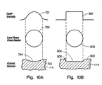
- Figs. 10A to 10B illustrate embodiments depicting laser beam power or intensity over a laser beam cross-section and the profile of the subsequently ablated material.
- Fig. 10A is an embodiment depicting a laser beam 700 with a Gaussian distribution of laser intensity.
- a Gaussian laser power or intensity curve 701 over the beam cross-section is shown.
- the laser beam 700 contacts a surface 702 of the material substantially within the area marked by the dashed lines.
- the laser beam 700 renders the ablated material with a curved surface 702.
- a central area 704 of the material is ablated to a larger degree than edge or periphery areas, due to the greater intensity of the laser beam in the center.
- the curved surface 702 may not be optimum due to the uneven topology.
- Fig. 10B illustrates an embodiment of a laser beam having uniform intensity for the laser beam power, or 'top hat' laser beams 800.
- a uniform laser power or intensity curve 801 over the beam cross-section is shown.
- the laser beam 800 contacts the surface 802 substantially within the dashed lines in Fig. 10B at surface 804. Even though the laser beam is not purposefully directed towards areas adjacent to surface 804, also known as edge or periphery areas 806, these areas 806 are affected in some embodiments.
- the laser beam 800 renders the ablated material with a substantially flat surface 804 in the area that the laser beam 800 directly contacts, and a curved surface along the periphery 806.
- the area 804 is substantially uniformly ablated, i.e. flat.
- the uniform intensity beam is achieved using (a) a beam expanding telescope, mask and imaging lens, (b) Diffractive Optical Elements and/or (c) beam homogeniser units (such as segmented mirrors).
- the present invention is not limited to thermally actuated printheads, but may also include, for example, piezoelectric activated printheads, and other mechanically actuated printheads, as well as other applications having micro-fluidic channels through a substrate.
- Methods of forming micro-fluidic channels described above may also be applied to micro-electromechanical, systems (MEMS) that include atomic resolution storage devices, fuel cells, sensors, and displays, for example.
- MEMS micro-electromechanical, systems
Landscapes
- Engineering & Computer Science (AREA)
- Physics & Mathematics (AREA)
- Optics & Photonics (AREA)
- Plasma & Fusion (AREA)
- Mechanical Engineering (AREA)
- Manufacturing & Machinery (AREA)
- Particle Formation And Scattering Control In Inkjet Printers (AREA)
- Laser Beam Processing (AREA)
Description
- This application claims the benefit of U.S. Provisional Application No. 60/343,476, filed on December 20, 2001, and U.S. Application No. 10/138,594, filed on May 2, 2002.
- The present invention relates to a method of laser machining a fluid channel according to preamble of claim 1. JP-06-079486 A discloses in combination all features of preamble of claim 1.
- Various inkjet printing arrangements are known in the art and include both thermally actuated printheads and mechanically actuated printheads. Thermal actuated printheads tend to use resistive elements or the like to achieve ink expulsion, while mechanically actuated printheads tend to use piezoelectric transducers or the like.
- A representative thermal inkjet printhead has a plurality of thin film resistors provided on a semiconductor substrate. An orifice and/or a barrier layer is provided on the substrate. The orifice and/or the barrier layer defines firing chambers about each of the resistors, an orifice corresponding to each resistor, and an entrance to each firing chamber. Actuation of a heater resistor by a "fire signal" causes ink in the corresponding firing chamber to be heated and expelled through the corresponding orifice.
- Ink typically is provided at the entrance of the firing chamber through a feed slot that is machined in the semiconductor substrate. The substrate usually has a rectangular shape, with the slot disposed longitudinally therein. Resistors are often arranged in rows located on one or both sides of the slot. The width of the print swath achieved by one pass of a printhead is approximately equal to the length of the resistor rows, which in turn is approximately equal to the length of the slot.
- Feed slots have typically been formed by sand drilling (also known as sandblasting or "sand slotting"). This method is a rapid, relatively simple and scalable process. The sand blasting method is capable of forming an opening in a substrate with a relatively high degree of accuracy for simple slot shapes, while generally avoiding substantial damage to surrounding components and materials. Also, it is capable of cutting openings in various substrates having different materials without the generation of excessive heat. Furthermore, it allows for improved relative placement accuracies during the production process.
- While sand slotting affords these apparent benefits, sand slotting is also disadvantageous in that it may cause microcracks in the semiconductor substrate that significantly reduce the substrate's fracture strength, resulting in significant yield loss due to cracked die. Low fracture strength also limits substrate length which in turn adversely impacts print swath height and overall print speed. In addition, sand slotting typically causes chips to the substrate on both the input and output side of the slot. Normally the chipping is tens of microns large and limits how close the firing chamber can be placed to the edge of the slot. Occasionally the chipping is larger and causes yield loss in the manufacturing process. The chipping problem is more prevalent as the desired slot length increases and the desired slot width decreases.
- Feed slots may also be formed by wet chemical etching with, for example, alkaline etchants. Such etching techniques result in etch angles that cause a very wide backside slot opening. The wide backside opening limits how small a particular die on the wafer could be and therefore limits the number of die per wafer (the separation ratio). It is desired to maximize the separation ratio.
- The invention consists in a method of laser machining a fluid channel according to claim 1.
-
- Fig. 1 illustrates a perspective view of an embodiment of a printer of the present invention;
- Fig. 2 illustrates a perspective view of an embodiment of a print cartridge of the present invention;
- Fig. 3 illustrates a perspective view of one embodiment of a printhead;
- Fig. 4 illustrates a cross-sectional view of an embodiment of a printhead of Fig. 2;
- Figs. 4A and 4B illustrate plan and perspective views of the printhead of Fig. 2;
- Figs. 5A to 5E illustrate process flow charts for several alternative embodiments of the manufacturing process for forming a slotted substrate according to the present invention;
- Figs. 6A to 6B illustrate one embodiment of steps toward forming the slotted substrate shown in profile;
- Fig. 6C illustrates one embodiment of the slotted substrate shown in profile and formed via steps shown in Figs. 6A to 6B;
- Fig. 6D illustrates another embodiment of the slotted substrate shown in profile and formed via steps shown in Figs. 6A to 6B;
- Figs. 6E to 6L illustrate various embodiments of slot profiles for the present invention;
- Figs. 7A to 7F illustrate various embodiments of laser beam patterns directed to a slot area on substrate surfaces in forming the slotted substrate of the present invention;
- Figs. 8A to 8B illustrate various embodiments of optical schemes for splitting the laser beam; and
- Figs. 9A to 9B illustrate one embodiment of steps to move the laser beam in the z-direction; and
- Figs. 10A to 10B illustrate embodiments depicting laser beam power and ablated material for laser beam cross-sections.
- Fig. 1 is a perspective view of a
printer 10 for printing onmedia 22 with a print cartridge (or ejection cartridge) 12. Fig. 2 is a perspective view of thecartridge 12 with a printhead (or fluid drop generator or fluid ejection device) 14 of an embodiment of the present invention. Fluid or ink is ejected or fired out fromnozzles 132 to themedia 22. - Fig. 3 illustrates an enlarged view of one embodiment of the
printhead 14 in perspective view. Theprinthead 14 in this embodiment has multiple features, including anedge step 119 for an edge fluid feed to resistors (or fluid ejectors) 61. The printhead also has atrench 124 that is partially formed into the substrate surface. A slot (or channel) 126 for a slot fluid feed toresistors 61, and/or a series ofholes 127 feeding fluid toresistors 61 are also shown on this printhead, each being formed by a UV laser machining process as described herein. Thetrench 124 may also be formed by the UV laser machining processes as described further below. In one embodiment there are at least two of the features described on theprinthead 14 in Fig. 3. For example, only the feed holes 127 and theslot 126 are formed in theprinthead 14, where in an alternative embodiment the edge step and/or thetrench 124 are formed as well. In another example, theedge step 119, and theslot 126 are formed in theprinthead 14, where in an alternative embodiment thetrench 124 and/or thefeedholes 127 are formed as well. - Fig. 4 illustrates a cross-sectional view of the
printhead 14 of Fig. 2 where theslot 126 having slot (or side)walls 123 is formed through asubstrate 102. The formation of the slot through a slot region (or slot area) in the substrate is described in more detail below. In another embodiment, a higher density of slots is etched in a given die. For example, the inter slot spacing or spacing between adjacent slots in the die or substrate are as low as 10 microns. (In an embodiment, 10 microns is just over twice the extent of a heat affected zone for each slot, where the heat affected zone is the area along the slot walls that is affected by the laser machining described in this application.) - In Fig. 4, a thin film layer (or an active layer, a thin film stack, an electrically conductive layer, or a layer with micro-electronics) 120 that is formed or deposited on a front or first side (or surface) 121 of the
substrate 102 is illustrated. Thefirst side 121 of the substrate is opposite a second side (or surface) 122 of thesubstrate 102. Thethin film stack 120 is at least one layer formed on the substrate, and, in a particular embodiment, masks at least a portion of thefirst side 121 of thesubstrate 102. Alternatively or additionally, the layer. 120 electrically insulates at least a portion of thefirst side 121 of thesubstrate 102. - As shown in the embodiment of the printhead shown in Fig. 4, the
thin film stack 120 includes acapping layer 104, aresistive layer 107, aconductive layer 108, apassivation layer 110, acavitation barrier layer 111, and abarrier layer 112, each formed or deposited over thefirst side 121 of thesubstrate 102 and/or the previous layer(s). In one embodiment, thesubstrate 102 is silicon. In various embodiments, the substrate is one of the following: single crystalline silicon, polycrystalline silicon, gallium arsenide, glass, silica, ceramics, or a semiconducting material. The various materials listed as possible substrate materials are not necessarily interchangeable and are selected depending upon the application for which they are to be used. In this embodiment, the thin film layers are patterned and etched, as appropriate, to form theresistors 61 in the resistive layer, conductive traces of the conductive layer, and afiring chamber 130 at least in part defined by the barrier layer. In a particular embodiment, thebarrier layer 112 defines thefiring chamber 130 where fluid is heated by the corresponding resistor and defines anozzle orifice 132 through which the heated fluid is ejected. In another embodiment, an orifice layer (not shown) having theorifices 132 is applied over thebarrier layer 112. An example of the physical arrangement of the barrier layer, and thin film substructure is illustrated at page 44 of the Hewlett-Packard Journal of February 1994. Further examples of ink jet printheads are set forth in commonly assigned U.S. Pat. No. 4,719,477, U.S. Pat. No. 5,317,346, and U.S. Pat. No. 6,162,589.In an alternative embodiment, at least one layer or thin film layer is formed or deposited upon thesubstrate 102. Embodiments of the present invention include having any number and type of layers formed or deposited over the substrate (or no layers at all), depending upon the application for which the slotted substrate is to be utilized. - In the embodiment shown in Fig. 4, a
channel 129 is formed as a hole orfluid feed slot 129 through the layers (120) formed upon the substrate. Thechannel 129 fluidically couples the firingchamber 130 and theslot 126, such that fluid flows through theslot 126 and into thefiring chamber 130 viachannel 129. In the particular embodiment shown, thechannel entrance 129 for the fluid is not in the center of theslot 126. However, the slotted substrate is formed as described below substantially the same in either instance where theentrance 129 is centrally located or off-center. - In the embodiment illustrated in Figs. 4A and 4B, a plan and a perspective view of the
printhead 14 and itsslot 126 is shown without the barrier layer 112 (for Fig. 4A) and without the stack 120 (for Fig. 4B). As shown in the embodiment of Fig. 4A, theresistors 61 are along theslot 126. As shown in the embodiment of Fig. 4B, theslot wall 123 has striations (or vertical lines) 142, and a rough area (or breakthrough area) 144 near the middle of theslot 126 formed by the slotting process of the present invention. Therough area 144 is formed by a breakthrough near the middle of theslot 126. The bending moment is minimized at this mid-slot location compared with a slot surface location, and therefore there is less stress on the breakthrough-rough area 144 during processing. As a result, cracking is minimized at the breakthrough-rough area 144, and thus throughout thesubstrate 102. Accordingly, slots formed by an embodiment of the present invention have chip sizes along the surfaces of the substrate of at most 3 microns, if any. - Also as shown in Figs. 4A and 4B, the
slot 126 has awall edge 146. In one embodiment, the roughness (or smoothness) of thewall edge 146 along thefront side 121 of the substrate is about 3 microns, and about 5 microns along thesecond side 122 of the substrate, although in the embodiment the roughness could be more or less. - In the embodiment described in the flow chart of Fig. 5A at
step 200, the thin film layer or stack 120 is formed, masked and patterned over thefirst side 121 of the wafer orsubstrate 102 to form therecess 129, as shown in Fig. 6A. In one embodiment (not shown), a hard mask and/or a photoimagable material layer are additionally formed on thebackside 122 of the substrate opposite thethin film layer 120. Atstep 210, the slot formation is begun using a UV laser beam 140 (See Fig. 6A) directed to an area of the substrate to be slotted. In this embodiment, an area on thesecond side 122 of the substrate is the initial area to be exposed to the UV laser beam. The substrate material in the area of the substrate that is exposed to the UV laser beam is ablated and/or vaporized to form the slot, 126, as described in more detail below. - As shown in Figs. 6A & 6B, debris or
residue 149 from the laser machining begins to form along theslot walls 123 as well as along the bottom of the trench being formed in the substrate. In alternative embodiments, the debris may be formed of polycrystalline and/or amorphous silicon oxide. As shown in the embodiment of Fig. 6B, at the end ofstep 210, thesubstrate 102 is laser machined to a depth x. - At
step 220, thelaser beam 140 is directed towards the first side orsurface 121 of the substrate through the recess in thethin film stack 120, as shown in Fig. 6B. The slot is completed by UV laser machining through the substrate to the depth y, where depth x is greater than depth y, where x + y = substrate depth. In a first embodiment, y is about 20 microns. In a second embodiment, x is about twice y. In a third embodiment, x is about the same as y. In yet another embodiment, y is greater than x. - At
step 230 of Fig. 5A, steps 210 and 220 are repeated for eachslot 126 in the die (or substrate). In the embodiment shown and described with regard to Figs. 6A and 6B, throughput is improved with the described bi-directional process because the debris (or redeposited material) 149 escapes the machined channel more readily in shallower rather than deeper trenches. Further, in embodiments where x is greater than y, the majority of the debris that escapes the machined channels escapes from thebackside 122, thereby limiting the amount of contamination to the active layer(s) 120 on thefront side 121 of the substrate. In another method, the UV laser etch is performed first from thefirst side 121, and then from thesecond side 122 to meet at thebreakthrough area 144. - In this embodiment, the laser machining is provided by a UV laser beam 140 (Fig. 6A), and in one particular embodiment, is provided by a diode-pumped solid-state pulsed UV laser. In another particular embodiment, the
UV laser 140 originates from aXise 200 Laser Machining Tool, manufactured by Xsil of Dublin, Ireland. A laser source 139 (shown in Figs. 9A and 9B) uses power in the range of about 2 to 100 Watts, and more particularly about 4.5 Watts. The laser beam has a wavelength of (1060 nm)/n or (1053 nm)/n, where n = 2, 3 or 4. In a specific embodiment, the UV wavelength is less than about 400 nm, in particular about 355 nm. The pulse width of the laser beam is about 15 ns in this embodiment, and the repetition rate is about 30 kHz. The laser beam has a diameter of about 5 to 100 microns, and more particularly about 30 microns in this embodiment. In an embodiment that is not shown here, the laser-machining tool of the present invention has a debris extraction system to remove thedebris 149 resulting from the laser machining. - In an embodiment of the present invention, the intense UV light is absorbed into less than about 1 micron of the surface of the material being ablated. Because the light energy is so concentrated near the surface of the material, the material rapidly heats, melts, and vaporizes. A mixture of vapor and molten droplets are then quickly ejected away. Consequently, the surrounding region (or heat affected zone) is not melted substantially or otherwise substantially damaged because the process happens so quickly, and there is not enough time for significant heat to propagate to the surrounding regions. A more in depth explanation of the process is described on pps. 131-134 of Laser-Beam Interactions with Materials: Physical Principles and Applications, 2nd updated edition, 1995, written by Martin von Allmen & Andreas Blatter.
- In the laser machining process of the current invention, smoother and more precise slot profiles are attainable because the laser machining is so localized. Accordingly, slots formed by embodiments of the present invention again have surface roughness of at most 5 microns. However, when the laser machine breaks through the substrate, and the
slot 126 is formed, there is likely to be the rough area orrough spot 144 near the breakthrough point, as shown in the embodiments of the slot profiles of Figs. 6C and 6D. In these embodiments, therough area 144 near the center of the slot is redeposited material caused by heated fragments that were not efficiently extracted due to the depth of the trench. These fragments subsequently melted and resolidified to form thedebris 149. - As depicted in Fig. 5B,
step 300 is similar to step 200 of Fig. 5A.Steps steps step 310, each slot on the die is partially formed from thesecond side 122. Then each partially formed slot is completed when the laser beam is directed towards thefirst side 121 instep 320. In other words, no repetition of previous steps occurs in this embodiment. In one embodiment, a beam splitter is used to partially form slots from the second side instep 310 and/or is used to complete slotting from the first side instep 320, wherein the beam splitter is discussed in more detail below with regard to Figs. 8A and 8B. In an alternative embodiment, thefirst side 121 is subjected to the laser machining process before thesecond side 122 thereby reversingsteps - As depicted in Fig. 5C,
step 400 is similar to step 200 of Fig. 5A. Instep 410, two or more slots on the die or wafer are partially formed simultaneously from thesecond side 122 of the die. Instep 420, those two ormore slots 126 are fully formed simultaneously from thefront side 121.Steps step 420, or partially formed instep 410, simultaneously through use of the beam splitters discussed below. In an alternative embodiment, thefirst side 121 is subjected to the laser machining process before thesecond side 122 thereby reversing thesteps - In another embodiment, the concepts of Figs. 5B and 5C can be combined such that two or more slots are partially formed simultaneously from the
second side 122. Then, each slot on the die is partially formed from the second side (in groups of two or more slots simultaneously) before any of the slots are fully formed by laser machining from the front side of the die (in groups of two or more slots simultaneously). In an alternative embodiment, thefirst side 121 is subjected to the laser machining process before thesecond side 122. - As depicted in Fig. 5D, steps 500, 510 and 520 are similar to
steps step 510, and then laser-machined from the first side of the substrate instep 520. After the slot is laser-machined from both sides, the slot is still not yet fully formed in that the laser machining has not fully broken through thesubstrate 102, as opposed to be completely formed afterstep 220. Instep 530, the partially formed slot is laser machined from the second side again, until breakthrough occurs. Instep 540,steps 510 to 530 are repeated for each slot on the die. As an alternative to step 540,step 510 is performed for each partially formed slot on the second side, then step 520 is performed for each partially formed slot on the first side, and then step 530 is performed for each partially formed slot on the second side until breakthrough occurs. In another alternative embodiment, the first side is partially laser machined, then the second side is partially laser machined, and then ultimate breakthrough occurs from the first side. - As depicted in Fig. 5E, steps 600 and 610 are similar to step 200 and 210 with some differences as follows. After
step 610 is performed, the laser machining from the second side breaks all the way through to the first surface of the substrate. Instep 620, thestep 610 is repeated for eachslot 126 to be formed in the die. In an alternative embodiment that is not shown, thebarrier layer 112 is formed with thethin film stack 120 over thefirst side 121 of the substrate instep 600. In another alternative embodiment,step 600 is performed afterstep 620 is completed. In another alternative embodiment, the UV laser machining of the slot is fully performed from thefirst side 121 of the substrate. - Figs. 6E to 6L illustrate various embodiments of a slot profile in a
substrate 102. In the embodiments shown, the slot profile is not to scale. Generally, the slot profile is narrower than as depicted. The slot profiles are depicted in these drawings as wider than in general for ease of viewing the distinctions in the slot profiles. Thesubstrate 102 is illustrated in these embodiments as having active layer (or layer with microelectronics) 120 on a first side of the substrate. However, in alternative embodiments, the active layer(s) 120 is on the second side of the substrate. In each of these embodiments shown, the slot profile is formed by one of the laser machining process described above, including a bi-directional laser machining process. - Fig. 6E illustrates an embodiment of the slotted
substrate 102 having steppedslot walls 128. Theslot walls 128 of Fig. 6E have varying cross-sectional areas that incrementally decrease from thesecond surface 122 to thefirst surface 121. In the illustrated embodiment, there are two steps and three varied cross-sectional areas associated with three slot widths a, b, and c. The slot width a is adjacent thefirst surface 121, the slot width c is adjacent thesecond surface 122, and the slot width b is in between a and c. In the embodiment shown, the slot width a is 210 microns, the slot width b is 220 microns, and the slot width c is 260 microns. In an alternative embodiment, the slot width near the first surface is in a range of about 5 to 100 microns, and the slot width near the second surface is in a range of about 100 to 300 microns, where the slot width near the second surface is greater than that of the first surface. In particular, the width near the second surface is at least 10% greater than that of the first surface. For example, the slot width near the second surface is about 140 microns, while the slot width near the first surface is about 50 microns. - In the embodiment shown in Fig. 6E, the slot profile is formed as follows: the slot widths b and c are formed from the
second side 122, then the slot width a is formed from thefirst side 121. In another embodiment, each of the slot widths are consecutively formed from thesecond side 122. In a first embodiment, the slot width a is formed, then slot width b, then slot width c. In a second embodiment, the slot width c is formed, then slot width b, then slot width a. However, various other embodiments are envisioned, including forming slot width b, then slot width c, then slot width a, especially when using bi-directional laser machining processes. - The stepped slot walls of the embodiment shown in Fig. 6E are formed by tracing the laser beam in a particular pattern over the particular side of the substrate. For example, Fig. 7E illustrates an embodiment where laser beams are traced in a multiple cookie-
cutter pattern 156 to form theslot 126. In this embodiment, the laser beams traced are substantially concentric elliptical shapes: shapes m, n, and p, where shape m is the smallest elliptical shape, and shape p is the largest elliptical shape as shown in Fig. 7E. In the embodiment described with respect to Fig. 6E, the shapes n and p are traced first, then the shape m is traced, where the shape m corresponds to the slot width a, the shape n corresponds to the slot width b, and the shape p corresponds to the slot width c. Other orders of tracing are envisioned with alternate embodiments of this invention. Additional embodiments of laser beam tracing patterns are illustrated in and described with respect to Figs. 7A to 7F. - Fig. 6F illustrates an embodiment of the slotted
substrate 102 having substantially tapered and smoothedslot walls 125. Theslot walls 125 of Fig. 6F have varying cross-sectional areas and incrementally decrease from thesecond surface 122 to thefirst surface 121. In the embodiment shown, as the slot profile approaches thefirst surface 121, the slot profile narrows and then expands slightly to thefirst surface 121. Because the slot profile narrows and expands near the first surface in this embodiment, there is a non-symmetrical hourglass shape with respect to the first and second surfaces of the substrate. The slot width adjacent the first surface is labeled as a. The slot width adjacent the second surface is labeled as c. The slot widths a and c of Fig. 6F are similar to the slot widths of Fig. 6E. - In one embodiment, the
slot walls 125 are formed by the method described with respect to Figs. 6A and 6B. When the substrate is laser-machined from the second side, and then laser-machined from the first side, the breakthrough area of the slot has the narrower cross-sectional area as described above and shown in Fig. 6F. - In another embodiment, the
slot walls 125 of Fig. 6F are formed by first forming the slot profile shown in Fig. 6E. In this embodiment, the steppedslot walls 128 are then smoothed out to form the taperedwalls 125 of Fig. 6F. Methods of smoothing are discussed in more detail below. In an alternative embodiment, the smoothed out walls have a slight curvature. In another embodiment, the slot profile tapers from thesecond surface 122 to thefirst surface 121 without the narrow cross-sectional area in the slot profile. - Fig. 6G illustrates an embodiment of the slot profile having a substantially hourglass-type shape, where the
narrowing section 144 near the middle is formed when the breakthrough in the silicon occurs. The slot has taperedwalls 125 that taper towards the middle of the slot from both the first and second surfaces of thesubstrate 102. This embodiment is generally formed with the bi-directional fluid slot formation described above with respect to flow chart Fig. 5A. - Fig. 6H illustrates an embodiment of the slot profile having substantially straight slot walls. These slot walls are formed using the smoothing methods described below. In one embodiment, these walls are formed by one of the methods described above.
- Fig. 61 illustrates an embodiment of the slot profile having a compound slot shape. Fig. 61 illustrates a slot profile having an hourglass-type shape with a counterbore in the second surface. The embodiment of the slot profile of Fig. 61 has wall surfaces 125 tapering from each substrate surface, as well as wall surfaces 128 that are stepped, i.e. orthogonal to the direction of the laser beam, forming the counterbore. In one embodiment, these
walls - Fig. 6J illustrates another embodiment of the slot profile having a compound slot shape. Fig. 6J illustrates a slot profile with a counterbore having a stepped
wall 128. Fig. 6J is similar to the embodiment described with respect to Fig. 6E, except Fig. 6J has only one step in the slot profile. The methods for forming Fig. 6E and other methods for forming slot walls described herein apply, as appropriate, to this current embodiment shown in Fig. 6J. - Fig. 6K illustrates an embodiment of the slot profile having a compound slot shape. Fig. 6K illustrates a slot profile having an hourglass-type shape with an offset counterbore. The embodiment of the slot profile of Fig. 6K has one slot wall with tapered
surfaces 125 as shown and described with respect to Fig. 6G, as well as one slot wall with a steppedsurface 128 and atapered surface 125 as shown and described with respect to Fig. 61. In one embodiment, these walls are formed by at least one of the methods described herein. - Fig. 6L illustrates another embodiment of the slot profile having a compound slot shape. Fig. 6L illustrates a slot profile with offset counterbores having stepped
walls 128. In the embodiment shown, the stepped walls on each side of the slot shift over in the same direction such that the cross-sectional area at substantially all points along the slot profile remains substantially the same. In one embodiment, these walls are formed by at least one of the methods described herein. - Figs. 7A to 7F illustrate various embodiments of laser beam patterns, including laser beam trace spacing. The laser beams are directed toward a slot area on either (or both) the
first surface 121 and thesecond surface 122 in forming the slotted substrates of the present invention. The applied laser beam patterns determine the slot areas, and thus, the slot shapes on the substrate surfaces. In a particular embodiment, a laser beam pattern is repeatedly applied to the substrate in forming the fluid feature. In another embodiment, multiple laser beam patterns are applied to the substrate in forming the fluid feature. In a first embodiment, the slot area on each side/surface of the substrate is about 260 microns x 8480 microns. In a second embodiment, the slot area on the first surface is about 210 microns x 8480 microns, and about 260 microns x 8480 microns on the second surface. In alternative embodiments, the slot widths are as narrow as 5 to 10 microns, and as wide as 300 microns. In more particular embodiments, the slot widths are 30-50 microns or 80 microns, depending upon the application of the fluid slot. In most embodiments, having a low aspect ratio increases the laser machining speed, due to debris interference associated with high aspect ratio features. In a particular embodiment, where slot widths as narrow as 5 to 10 microns are desired, debris accumulation along the slot walls is much greater than slot widths of greater than about 80 microns. - Fig. 7A illustrates an embodiment where laser beams are traced in a raster or
serpentine pattern 150 to form theslot 126 in theprinthead 14. In the embodiment shown, the laser beams are traced starting at one end of the slot area, then traced back and forth in the longitudinal direction until reaching the opposite longitudinal end of the slot. As shown in this embodiment, the spacing between adjacent laser beam traces is substantially constant. - Fig. 7B illustrates an embodiment where laser beams are traced in a substantially
spiral pattern 152 to form theslot 126. The laser beams are traced starting at the center of the slot and move in a circular pattern gradually increasing in size to form theslot 126 shape. In an alternative embodiment, the laser beams are traced starting along the edges of the desired slot shape and gradually decreasing in size while moving in a substantially circular pattern. - Fig. 7C illustrates an embodiment where laser beams are traced in a
cookie cutter pattern 154 to form theslot 126. In the embodiment shown, the laser beams are traced along the edges of the desired slot shape of theslot 126. - Fig. 7D illustrates an embodiment where laser beams are traced in a
cookie cutter pattern 154, as described and shown with respect to Fig. 7C, as well as theraster pattern 150, as described and shown with respect to Fig. 7A, to form theslot 126. Eitherpattern - The embodiment of Fig. 7E for forming a slot using the multiple cookie-cutter
laser beam pattern 156 has previously been described. In an alternative embodiment, there are a plurality of traces in the cookie-cutter laser beam pattern, such as two traces, or as many as practically possible. For embodiments such as those shown in Fig. 6E, the laser beam traces become successively smaller (or larger), and successive laser beams are directed to a lower (or higher) depth in the substrate. As the number of successive laser beam traces (that vary in size and depth slightly from the last) increase, the slot walls increasingly become smoother. - Fig. 7F illustrates an embodiment where laser beams are traced in a modified
window pattern 158 to form theslot 126. In the embodiment shown, the laser beam is traced in a closed loop within the edges of the desired slot shape of theslot 126. In a first embodiment each consecutive laser beam trace is larger than the previous closed loop. In a second embodiment, each consecutive laser beam trace is smaller than the previous closed loop. However, as shown, the spacing between consecutive traces is maintained substantially constant except near the end of the slot. In the embodiment shown, the closed loop of each consecutive laser beam trace overlaps on each slot end. In this embodiment, there are 4 closed loops overlapping at each slot end. In alternative embodiments, there are at least 2 closed loops. - Various embodiments of slot profiles that combine steps, tapered walls, smooth walls, and counterbores are envisioned with the present invention.
- In alternative embodiments or embodiments additional to the laser beam trace pattern, the stepped, tapered, smooth or otherwise varied slot walls of the embodiments shown in Figs. 6A through 6L are formed by varying the laser process, trace, or laser beam source. There are several methods of varying the laser beam or the laser process that may be employed with embodiments of the present invention. Some of the methods include varying the laser beam diameter by moving the laser beam focus in a z-direction (towards or away from the substrate), and adjusting the UV laser machine. For example, the laser beam diameter may be varied using a beam expander. In a particular embodiment, the beam expander (telescope) is Galilean, where there is no internal focus that can lead to air break down with high energy pulsed lasers. Alternatively, Keplerian telescopes are used at lower energies. For more information on beam expanders that may be used with this invention, see http://www.mellesgriot.com/pdf/002.10-2.12.pdf. A scan speed, a pulse width, a repetition rate, focusing lens, laser power, etc., may be adjusted on the UV laser machine to vary the laser beam or laser process. For example, the laser power may be reduced at or near surface breakthrough to minimize damage, including chipping and cracking, to the substrate surface (especially for reducing damage to slot edges in the surface with active layers). In another example, the laser beam is defocused in order to clean the slot and the substrate.
- Figs. 8A to 8B illustrate various embodiments of optical schemes for splitting the
laser beam 140. In these illustrated embodiments, thelaser beam 140 comes from thelaser source 139. The high-energypulse laser beam 140 is split into a number of beamlets such that the energy of each beamlet has optimum energy, and hence optimum etch depth. In the embodiments shown, increases in laser power are used to produce two beams with more optimal conditions. Fig. 8A illustrates splitting the beam using conventional optics, while Fig. 8B illustrates an alternative embodiment of splitting the beam using diffractive optics. Provided large enough optics are used, embodiments of the present invention are applicable to beams of any size. In other embodiments, more than two beams or beamlets having the optimum energy are envisioned with the present invention. - Fig. 8A illustrates the embodiment where the
laser beam 140 hits a 50/50beam splitter 180, where the beam splits into two beamlets. A first one of the beamlets continues in the same direction and, upon reaching a first focusinglens 184, is focused to the printhead 14 (or substrate) for laser machining the substrate. A second one of the beamlets is deflected in a perpendicular direction and the beamlet subsequently hits amirror 182 and is deflected towards a second focusinglens 184 to be focused to the printhead (or substrate) adjacent the first of the beamlets. In this manner, two laser beams are able to machine two slots on a substrate simultaneously. - Fig. 8B illustrates splitting the beam using diffractive optics. Fig. 8B illustrates the embodiment where the
laser beam 140 hits adiffractive element 186, where the beam splits into two beamlets. Each of the two beamlets continues in substantially the same direction towards the substrate to a focusinglens 184. The laser beamlets are then focused to slot areas or areas to be laser machined on the substrate orprinthead 14. In this alternative manner, two laser beams are able to machine two slots or two areas on a substrate simultaneously. - Figs. 9A to 9B illustrate one embodiment of steps to move the laser beam focal point in the z-direction. In this embodiment, the
laser source 139 of thelaser beam 140 is moved from a first position relative to thesubstrate 102, shown in Fig. 9A, to a closer position relative to thesubstrate 102, shown in Fig. 9B. In the embodiment shown, as the laser beam machines through the substrate and the etch depth increases, the distance between the laser source and the substrate being etched increases. Consequently, in the embodiment shown, the focus of the laser beam is altered non-optimally (due to beam attenuation) and/or the amount ofdebris 149 increases. As shown in the embodiment of Fig. 9B, if the laser source is moved with the depth etch, the focus of the laser beam remains substantially the same throughout. In an alternative embodiment, the laser beam focal point is adjusted with the increasing depth. - Figs. 10A to 10B illustrate embodiments depicting laser beam power or intensity over a laser beam cross-section and the profile of the subsequently ablated material. Fig. 10A is an embodiment depicting a
laser beam 700 with a Gaussian distribution of laser intensity. In Fig. 10A, a Gaussian laser power orintensity curve 701 over the beam cross-section is shown. Thelaser beam 700 contacts asurface 702 of the material substantially within the area marked by the dashed lines. In this embodiment, thelaser beam 700 renders the ablated material with acurved surface 702. Acentral area 704 of the material is ablated to a larger degree than edge or periphery areas, due to the greater intensity of the laser beam in the center. In some embodiments, thecurved surface 702 may not be optimum due to the uneven topology. - Fig. 10B illustrates an embodiment of a laser beam having uniform intensity for the laser beam power, or 'top hat'
laser beams 800. In Fig. 10B, a uniform laser power orintensity curve 801 over the beam cross-section is shown. In this embodiment, thelaser beam 800 contacts thesurface 802 substantially within the dashed lines in Fig. 10B atsurface 804. Even though the laser beam is not purposefully directed towards areas adjacent to surface 804, also known as edge orperiphery areas 806, theseareas 806 are affected in some embodiments. As shown in this embodiment, thelaser beam 800 renders the ablated material with a substantiallyflat surface 804 in the area that thelaser beam 800 directly contacts, and a curved surface along theperiphery 806. Due to the uniform intensity of the laser beam substantially along the entire cross-section, thearea 804 is substantially uniformly ablated, i.e. flat. In some embodiments, the uniform intensity beam is achieved using (a) a beam expanding telescope, mask and imaging lens, (b) Diffractive Optical Elements and/or (c) beam homogeniser units (such as segmented mirrors). - It is therefore to be understood that this invention may be practiced otherwise than as specifically described. For example, the present invention is not limited to thermally actuated printheads, but may also include, for example, piezoelectric activated printheads, and other mechanically actuated printheads, as well as other applications having micro-fluidic channels through a substrate. Methods of forming micro-fluidic channels described above may also be applied to micro-electromechanical, systems (MEMS) that include atomic resolution storage devices, fuel cells, sensors, and displays, for example. Thus, the present embodiments of the invention should be considered in all respects as illustrative and not restrictive, the scope of the invention to be indicated by the appended claims rather than the foregoing description. Where the claims recite "a" or "a first" element of the equivalent thereof, such claims should be understood to include incorporation of one or more such elements, neither requiring nor excluding two or more such elements.
Claims (3)
- A method of laser machining a fluid channel comprising:directing a UV laser beam towards a substrate to form a fluid channel through the substrate,wherein the substrate has a first surface with a first channel area and an opposite second surface with a second channel area,wherein the laser beam is directed towards the first and second channel areas for bi-directional laser machining of the fluid channel,wherein the bi-directional machining limits contamination to the active layers, characterised in thatthe first surface has active layers andthe second surface is laser-machined before the first surface.
- The method of claim 1, wherein the active layers are microelectronics.
- The method of claim 1 or claim 2, wherein a majority of the fluid channel is laser-machined from the second surface.
Priority Applications (1)
| Application Number | Priority Date | Filing Date | Title |
|---|---|---|---|
| EP06076894A EP1769872A3 (en) | 2001-12-20 | 2002-06-21 | Method of laser machining a fluid slot |
Applications Claiming Priority (5)
| Application Number | Priority Date | Filing Date | Title |
|---|---|---|---|
| US34347601P | 2001-12-20 | 2001-12-20 | |
| US343476P | 2001-12-20 | ||
| US138594 | 2002-05-02 | ||
| US10/138,594 US7357486B2 (en) | 2001-12-20 | 2002-05-02 | Method of laser machining a fluid slot |
| PCT/US2002/019752 WO2003053627A1 (en) | 2001-12-20 | 2002-06-21 | Method of laser machining a fluid slot |
Related Child Applications (1)
| Application Number | Title | Priority Date | Filing Date |
|---|---|---|---|
| EP06076894A Division EP1769872A3 (en) | 2001-12-20 | 2002-06-21 | Method of laser machining a fluid slot |
Publications (2)
| Publication Number | Publication Date |
|---|---|
| EP1455986A1 EP1455986A1 (en) | 2004-09-15 |
| EP1455986B1 true EP1455986B1 (en) | 2006-12-27 |
Family
ID=26836344
Family Applications (1)
| Application Number | Title | Priority Date | Filing Date |
|---|---|---|---|
| EP02747939A Expired - Lifetime EP1455986B1 (en) | 2001-12-20 | 2002-06-21 | Method of laser machining a fluid slot |
Country Status (7)
| Country | Link |
|---|---|
| US (1) | US7357486B2 (en) |
| EP (1) | EP1455986B1 (en) |
| JP (1) | JP4302527B2 (en) |
| CN (1) | CN1738693B (en) |
| AU (1) | AU2002318383A1 (en) |
| DE (1) | DE60217172T2 (en) |
| WO (1) | WO2003053627A1 (en) |
Families Citing this family (21)
| Publication number | Priority date | Publication date | Assignee | Title |
|---|---|---|---|---|
| US20030155328A1 (en) * | 2002-02-15 | 2003-08-21 | Huth Mark C. | Laser micromachining and methods and systems of same |
| US6958106B2 (en) * | 2003-04-09 | 2005-10-25 | Endicott International Technologies, Inc. | Material separation to form segmented product |
| US7893386B2 (en) * | 2003-11-14 | 2011-02-22 | Hewlett-Packard Development Company, L.P. | Laser micromachining and methods of same |
| GB2410465A (en) * | 2004-01-29 | 2005-08-03 | Hewlett Packard Development Co | Method of making an inkjet printhead |
| US20050219327A1 (en) * | 2004-03-31 | 2005-10-06 | Clarke Leo C | Features in substrates and methods of forming |
| US7268315B2 (en) * | 2005-07-13 | 2007-09-11 | Hewlett-Packard Development Company, L.P. | Monitoring slot formation in substrates |
| WO2007043963A1 (en) * | 2005-10-13 | 2007-04-19 | Silex Microsystems Ab | Fabrication of inlet and outlet connections for microfluidic chips |
| FR2909297B1 (en) * | 2006-11-30 | 2010-03-05 | Snecma | METHOD FOR LASER DRILLING OF A PIECE OF COMPOSITE MATERIAL WITH CERAMIC MATRIX, HOLE OBTAINED BY THIS PROCESS, PIECE OF COMPOSITE MATERIAL WITH CERAMIC MATRIX COMPRISING IT, TURBOREACTOR COMPRISING SUCH A PIECE |
| US7855151B2 (en) * | 2007-08-21 | 2010-12-21 | Hewlett-Packard Development Company, L.P. | Formation of a slot in a silicon substrate |
| JP5405859B2 (en) * | 2009-03-12 | 2014-02-05 | 株式会社ディスコ | Ink reservoir processing method for ink jet printer head |
| DE102010011508B4 (en) * | 2010-03-15 | 2015-12-10 | Ewag Ag | Method for producing at least one flute and at least one cutting edge and laser processing device |
| EP2452775A1 (en) * | 2010-11-16 | 2012-05-16 | Siemens Aktiengesellschaft | Shortened method for drilling a hole |
| JP5857548B2 (en) * | 2011-09-02 | 2016-02-10 | 株式会社リコー | Thin film manufacturing method, electromechanical transducer manufacturing method, and liquid discharge head manufacturing method |
| WO2013095430A1 (en) * | 2011-12-21 | 2013-06-27 | Hewlett Packard Development Company, L.P. | Fluid dispenser |
| CN102769083A (en) * | 2012-07-16 | 2012-11-07 | 江苏扬景光电有限公司 | Flip-chip bonding nitride light emitting diode (LED), light-transmission substrate thereof, and methods for manufacturing light-transmission substrate |
| US9991090B2 (en) * | 2012-11-15 | 2018-06-05 | Fei Company | Dual laser beam system used with an electron microscope and FIB |
| JP6318171B2 (en) * | 2012-12-20 | 2018-04-25 | エレクトロ サイエンティフィック インダストリーズ インコーポレーテッド | Method for forming an image by laser micromachining |
| CN103240526B (en) * | 2013-05-10 | 2015-06-10 | 中国电子科技集团公司第五十四研究所 | Laser boring method based on nanoscale particle flow |
| US10357848B2 (en) * | 2015-01-19 | 2019-07-23 | General Electric Company | Laser machining systems and methods |
| US10580725B2 (en) * | 2017-05-25 | 2020-03-03 | Corning Incorporated | Articles having vias with geometry attributes and methods for fabricating the same |
| CN109352185B (en) * | 2018-10-23 | 2021-03-09 | 深圳赛意法微电子有限公司 | Beam splitting laser cutting method for silicon carbide-based wafer |
Family Cites Families (53)
| Publication number | Priority date | Publication date | Assignee | Title |
|---|---|---|---|---|
| IL67599A (en) * | 1982-12-31 | 1986-09-30 | Laser Ind Ltd | Control apparatus particularly useful for controlling a laser |
| US4746935A (en) | 1985-11-22 | 1988-05-24 | Hewlett-Packard Company | Multitone ink jet printer and method of operation |
| US4719477A (en) * | 1986-01-17 | 1988-01-12 | Hewlett-Packard Company | Integrated thermal ink jet printhead and method of manufacture |
| JPS62234687A (en) | 1986-04-03 | 1987-10-14 | Inoue Japax Res Inc | Manufacture of die |
| US4915981A (en) | 1988-08-12 | 1990-04-10 | Rogers Corporation | Method of laser drilling fluoropolymer materials |
| DE3934587C2 (en) | 1989-10-17 | 1998-11-19 | Bosch Gmbh Robert | Process for producing high-precision through holes in workpieces generated by laser radiation |
| US5385633A (en) | 1990-03-29 | 1995-01-31 | The United States Of America As Represented By The Secretary Of The Navy | Method for laser-assisted silicon etching using halocarbon ambients |
| US5322988A (en) | 1990-03-29 | 1994-06-21 | The United States Of America As Represented By The Secretary Of The Navy | Laser texturing |
| US5354420A (en) | 1990-03-29 | 1994-10-11 | The United States Of America As Represented By The Secretary Of The Navy | Method for laser-assisted etching of III-V and II-VI semiconductor compounds using chlorofluorocarbon ambients |
| US5362450A (en) | 1990-03-29 | 1994-11-08 | The United States Of America As Represented By The Secretary Of The Navy | Laser controlled decomposition of chlorofluorocarbons |
| US5266532A (en) | 1990-03-29 | 1993-11-30 | The United States Of America As Represented By The Secretary Of The Navy | Method for laser-assisted silicon etching using halocarbon ambients |
| US5688715A (en) | 1990-03-29 | 1997-11-18 | The United States Of America As Represented By The Secretary Of The Navy | Excimer laser dopant activation of backside illuminated CCD's |
| US5493445A (en) | 1990-03-29 | 1996-02-20 | The United States Of America As Represented By The Secretary Of The Navy | Laser textured surface absorber and emitter |
| US5469199A (en) | 1990-08-16 | 1995-11-21 | Hewlett-Packard Company | Wide inkjet printhead |
| US5293025A (en) | 1991-08-01 | 1994-03-08 | E. I. Du Pont De Nemours And Company | Method for forming vias in multilayer circuits |
| US5397863A (en) | 1991-09-13 | 1995-03-14 | International Business Machines Corporation | Fluorinated carbon polymer composites |
| JPH05144978A (en) | 1991-11-20 | 1993-06-11 | Fujitsu Ltd | Formation of via-holes in silicon substrate and manufacture of multichip module |
| JPH05147223A (en) * | 1991-12-02 | 1993-06-15 | Matsushita Electric Ind Co Ltd | Ink jet head |
| US5211806A (en) | 1991-12-24 | 1993-05-18 | Xerox Corporation | Monolithic inkjet printhead |
| US5317346A (en) * | 1992-03-04 | 1994-05-31 | Hewlett-Packard Company | Compound ink feed slot |
| US5297331A (en) * | 1992-04-03 | 1994-03-29 | Hewlett-Packard Company | Method for aligning a substrate with respect to orifices in an inkjet printhead |
| JP3290495B2 (en) | 1992-04-21 | 2002-06-10 | キヤノン株式会社 | Method of manufacturing ink jet recording head |
| JP3127570B2 (en) | 1992-05-25 | 2001-01-29 | セイコーエプソン株式会社 | Method of manufacturing inkjet head |
| JPH0679486A (en) | 1992-08-25 | 1994-03-22 | Rohm Co Ltd | Working method for ink jet head |
| KR0127666B1 (en) | 1992-11-25 | 1997-12-30 | 모리시다 요이찌 | Ceramic electronic device and method of producing the same |
| DE4241045C1 (en) | 1992-12-05 | 1994-05-26 | Bosch Gmbh Robert | Process for anisotropic etching of silicon |
| US5387314A (en) | 1993-01-25 | 1995-02-07 | Hewlett-Packard Company | Fabrication of ink fill slots in thermal ink-jet printheads utilizing chemical micromachining |
| DE69622217T2 (en) | 1995-04-14 | 2002-12-05 | Canon K.K., Tokio/Tokyo | A method of manufacturing a liquid ejection head and a liquid ejection head made by this method |
| JPH08300667A (en) | 1995-05-11 | 1996-11-19 | Brother Ind Ltd | Production of ink jet head |
| DE19534590A1 (en) | 1995-09-11 | 1997-03-13 | Laser & Med Tech Gmbh | Scanning ablation of ceramic materials, plastics and biological hydroxyapatite materials, especially hard tooth substance |
| US6162589A (en) * | 1998-03-02 | 2000-12-19 | Hewlett-Packard Company | Direct imaging polymer fluid jet orifice |
| GB2311953A (en) | 1996-03-23 | 1997-10-15 | British Aerospace | Laser beam drilling |
| WO1998020533A2 (en) | 1996-11-08 | 1998-05-14 | W.L. Gore & Associates, Inc. | Method for using photoabsorptive coatings to enhance both blind and through micro-via entrance quality |
| JPH10163136A (en) | 1996-12-04 | 1998-06-19 | Unisia Jecs Corp | Method for machining silicon wafer |
| US5835513A (en) * | 1997-01-08 | 1998-11-10 | Spectra Physics, Inc. | Q-switched laser system providing UV light |
| US6624382B2 (en) * | 1997-01-30 | 2003-09-23 | Anvik Corporation | Configured-hole high-speed drilling system for micro-via pattern formation, and resulting structure |
| US5870421A (en) | 1997-05-12 | 1999-02-09 | Dahm; Jonathan S. | Short pulsewidth, high pulse repetition frequency laser system |
| JPH118222A (en) | 1997-06-16 | 1999-01-12 | Seiko Epson Corp | Method of processing silicon substrate |
| DE19736370C2 (en) | 1997-08-21 | 2001-12-06 | Bosch Gmbh Robert | Process for anisotropic etching of silicon |
| US6563079B1 (en) | 1999-02-25 | 2003-05-13 | Seiko Epson Corporation | Method for machining work by laser beam |
| JP2000246475A (en) | 1999-02-25 | 2000-09-12 | Seiko Epson Corp | Machining method by means of laser beams |
| IT1310099B1 (en) | 1999-07-12 | 2002-02-11 | Olivetti Lexikon Spa | MONOLITHIC PRINT HEAD AND RELATED MANUFACTURING PROCESS. |
| IE20000618A1 (en) | 1999-08-03 | 2001-03-07 | Xsil Technology Ltd | A circuit singulation system and method |
| US6310701B1 (en) | 1999-10-08 | 2001-10-30 | Nanovia Lp | Method and apparatus for ablating high-density array of vias or indentation in surface of object |
| CN2399865Y (en) * | 1999-10-18 | 2000-10-04 | 福建华科光电有限公司 | Microchip laser |
| US6472125B1 (en) | 1999-11-30 | 2002-10-29 | Canon Kabushiki Kaisha | Method for manufacturing ink jet recording head and ink jet recording head manufactured by such method of manufacture |
| IT1309735B1 (en) | 1999-12-27 | 2002-01-30 | Olivetti Lexikon Spa | INK MULTIPLE CHANNEL HEAD |
| WO2001074529A2 (en) | 2000-03-30 | 2001-10-11 | Electro Scientific Industries, Inc. | Laser system and method for single pass micromachining of multilayer workpieces |
| WO2002034455A1 (en) | 2000-10-26 | 2002-05-02 | Xsil Technology Limited | Control of laser machining |
| KR20030064808A (en) | 2000-12-15 | 2003-08-02 | 엑스에스아이엘 테크놀러지 리미티드 | Laser machining of semiconductor materials |
| US6481832B2 (en) * | 2001-01-29 | 2002-11-19 | Hewlett-Packard Company | Fluid-jet ejection device |
| DE60210770T2 (en) | 2001-03-22 | 2006-08-31 | Xsil Technology Ltd. | A LASER PROCESSING SYSTEM AND METHOD |
| CN100369235C (en) | 2001-10-01 | 2008-02-13 | 埃克赛尔技术有限公司 | Machining substrates, particularly semiconductor wafers |
-
2002
- 2002-05-02 US US10/138,594 patent/US7357486B2/en not_active Expired - Fee Related
- 2002-06-21 EP EP02747939A patent/EP1455986B1/en not_active Expired - Lifetime
- 2002-06-21 DE DE60217172T patent/DE60217172T2/en not_active Expired - Fee Related
- 2002-06-21 AU AU2002318383A patent/AU2002318383A1/en not_active Abandoned
- 2002-06-21 JP JP2003554378A patent/JP4302527B2/en not_active Expired - Fee Related
- 2002-06-21 CN CN028258568A patent/CN1738693B/en not_active Expired - Fee Related
- 2002-06-21 WO PCT/US2002/019752 patent/WO2003053627A1/en active IP Right Grant
Also Published As
| Publication number | Publication date |
|---|---|
| US7357486B2 (en) | 2008-04-15 |
| WO2003053627A1 (en) | 2003-07-03 |
| AU2002318383A1 (en) | 2003-07-09 |
| JP2005512848A (en) | 2005-05-12 |
| US20030117449A1 (en) | 2003-06-26 |
| CN1738693B (en) | 2010-06-16 |
| JP4302527B2 (en) | 2009-07-29 |
| CN1738693A (en) | 2006-02-22 |
| DE60217172D1 (en) | 2007-02-08 |
| DE60217172T2 (en) | 2007-10-11 |
| EP1455986A1 (en) | 2004-09-15 |
Similar Documents
| Publication | Publication Date | Title |
|---|---|---|
| EP1455986B1 (en) | Method of laser machining a fluid slot | |
| KR100508193B1 (en) | Inkject print nozzle plates | |
| EP1353773B1 (en) | Method of and system for laser milling | |
| US6749285B2 (en) | Method of milling repeatable exit holes in ink-jet nozzles | |
| US8653410B2 (en) | Method of forming substrate for fluid ejection device | |
| EP1503901B1 (en) | Surface characteristic apparatus and method | |
| JP2006051820A (en) | Formation of featured parts in printhead components | |
| KR100340271B1 (en) | Laser working method, method for producing ink jet recording head utilizing the same, and ink jet recording head produced by such method | |
| US20040075717A1 (en) | Wafer processing apparatus and method | |
| US7302309B2 (en) | Laser micromachining methods and systems | |
| EP1769872A2 (en) | Method of laser machining a fluid slot | |
| EP1817135A1 (en) | Laser micromachining methods and systems using a liquid as an assist medium | |
| EP1525070A1 (en) | Inkjet nozzle and process of laser drilling a hole for use in inkjet nozzles | |
| JP6991760B2 (en) | How to process a silicon substrate | |
| CN109195804B (en) | Thermal inkjet printhead and method of manufacturing the same | |
| JP2007203650A (en) | Method for manufacturing droplet discharge head | |
| Dahotre et al. | Laser Micromachining |
Legal Events
| Date | Code | Title | Description |
|---|---|---|---|
| PUAI | Public reference made under article 153(3) epc to a published international application that has entered the european phase |
Free format text: ORIGINAL CODE: 0009012 |
|
| 17P | Request for examination filed |
Effective date: 20040615 |
|
| AK | Designated contracting states |
Kind code of ref document: A1 Designated state(s): AT BE CH CY DE DK ES FI FR GB GR IE IT LI LU MC NL PT SE TR |
|
| AX | Request for extension of the european patent |
Extension state: AL LT LV MK RO SI |
|
| RIN1 | Information on inventor provided before grant (corrected) |
Inventor name: SCOTT, GRAEME Inventor name: CAHILL, DAVID Inventor name: MCLOUGHLIN, NOEL Inventor name: POLLARD, JEFFREY, R. Inventor name: O'REILLY, DECLAN, JOHN |
|
| 17Q | First examination report despatched |
Effective date: 20050401 |
|
| GRAP | Despatch of communication of intention to grant a patent |
Free format text: ORIGINAL CODE: EPIDOSNIGR1 |
|
| GRAS | Grant fee paid |
Free format text: ORIGINAL CODE: EPIDOSNIGR3 |
|
| GRAA | (expected) grant |
Free format text: ORIGINAL CODE: 0009210 |
|
| AK | Designated contracting states |
Kind code of ref document: B1 Designated state(s): DE FR GB IE IT NL |
|
| REG | Reference to a national code |
Ref country code: GB Ref legal event code: FG4D |
|
| REG | Reference to a national code |
Ref country code: IE Ref legal event code: FG4D |
|
| REF | Corresponds to: |
Ref document number: 60217172 Country of ref document: DE Date of ref document: 20070208 Kind code of ref document: P |
|
| ET | Fr: translation filed | ||
| PLBE | No opposition filed within time limit |
Free format text: ORIGINAL CODE: 0009261 |
|
| STAA | Information on the status of an ep patent application or granted ep patent |
Free format text: STATUS: NO OPPOSITION FILED WITHIN TIME LIMIT |
|
| 26N | No opposition filed |
Effective date: 20070928 |
|
| PGFP | Annual fee paid to national office [announced via postgrant information from national office to epo] |
Ref country code: IE Payment date: 20090626 Year of fee payment: 8 Ref country code: NL Payment date: 20090624 Year of fee payment: 8 |
|
| PGFP | Annual fee paid to national office [announced via postgrant information from national office to epo] |
Ref country code: DE Payment date: 20090629 Year of fee payment: 8 |
|
| PGFP | Annual fee paid to national office [announced via postgrant information from national office to epo] |
Ref country code: FR Payment date: 20100630 Year of fee payment: 9 |
|
| PGFP | Annual fee paid to national office [announced via postgrant information from national office to epo] |
Ref country code: IT Payment date: 20100624 Year of fee payment: 9 |
|
| PGFP | Annual fee paid to national office [announced via postgrant information from national office to epo] |
Ref country code: GB Payment date: 20100401 Year of fee payment: 9 |
|
| REG | Reference to a national code |
Ref country code: NL Ref legal event code: V1 Effective date: 20110101 |
|
| PG25 | Lapsed in a contracting state [announced via postgrant information from national office to epo] |
Ref country code: IE Free format text: LAPSE BECAUSE OF NON-PAYMENT OF DUE FEES Effective date: 20100621 Ref country code: DE Free format text: LAPSE BECAUSE OF NON-PAYMENT OF DUE FEES Effective date: 20110101 |
|
| PG25 | Lapsed in a contracting state [announced via postgrant information from national office to epo] |
Ref country code: NL Free format text: LAPSE BECAUSE OF NON-PAYMENT OF DUE FEES Effective date: 20110101 |
|
| GBPC | Gb: european patent ceased through non-payment of renewal fee |
Effective date: 20110621 |
|
| PG25 | Lapsed in a contracting state [announced via postgrant information from national office to epo] |
Ref country code: IT Free format text: LAPSE BECAUSE OF NON-PAYMENT OF DUE FEES Effective date: 20110621 |
|
| REG | Reference to a national code |
Ref country code: FR Ref legal event code: ST Effective date: 20120229 |
|
| PG25 | Lapsed in a contracting state [announced via postgrant information from national office to epo] |
Ref country code: FR Free format text: LAPSE BECAUSE OF NON-PAYMENT OF DUE FEES Effective date: 20110630 |
|
| PG25 | Lapsed in a contracting state [announced via postgrant information from national office to epo] |
Ref country code: GB Free format text: LAPSE BECAUSE OF NON-PAYMENT OF DUE FEES Effective date: 20110621 |