EP1453308B1 - Abbildungsvorrichtung - Google Patents
Abbildungsvorrichtung Download PDFInfo
- Publication number
- EP1453308B1 EP1453308B1 EP04250371.4A EP04250371A EP1453308B1 EP 1453308 B1 EP1453308 B1 EP 1453308B1 EP 04250371 A EP04250371 A EP 04250371A EP 1453308 B1 EP1453308 B1 EP 1453308B1
- Authority
- EP
- European Patent Office
- Prior art keywords
- fields
- field
- image pick
- imaging apparatus
- colour image
- Prior art date
- Legal status (The legal status is an assumption and is not a legal conclusion. Google has not performed a legal analysis and makes no representation as to the accuracy of the status listed.)
- Expired - Lifetime
Links
- 238000003384 imaging method Methods 0.000 title claims description 14
- 238000012545 processing Methods 0.000 claims description 13
- 239000003086 colorant Substances 0.000 claims description 3
- 238000000034 method Methods 0.000 description 14
- 230000008569 process Effects 0.000 description 14
- 238000010586 diagram Methods 0.000 description 13
- 101100115215 Caenorhabditis elegans cul-2 gene Proteins 0.000 description 12
- 238000012544 monitoring process Methods 0.000 description 8
- 238000011156 evaluation Methods 0.000 description 5
- 230000006870 function Effects 0.000 description 4
- 230000035945 sensitivity Effects 0.000 description 3
- 230000006835 compression Effects 0.000 description 2
- 238000007906 compression Methods 0.000 description 2
- 230000006837 decompression Effects 0.000 description 2
- 230000003287 optical effect Effects 0.000 description 2
- 230000009467 reduction Effects 0.000 description 2
- 238000012546 transfer Methods 0.000 description 2
- 230000008859 change Effects 0.000 description 1
- 238000006243 chemical reaction Methods 0.000 description 1
- 230000002596 correlated effect Effects 0.000 description 1
- 239000013078 crystal Substances 0.000 description 1
- 230000004907 flux Effects 0.000 description 1
- 239000004973 liquid crystal related substance Substances 0.000 description 1
- 230000002093 peripheral effect Effects 0.000 description 1
- 238000011112 process operation Methods 0.000 description 1
- 238000005070 sampling Methods 0.000 description 1
- 239000007787 solid Substances 0.000 description 1
Images



Classifications
-
- H—ELECTRICITY
- H04—ELECTRIC COMMUNICATION TECHNIQUE
- H04N—PICTORIAL COMMUNICATION, e.g. TELEVISION
- H04N23/00—Cameras or camera modules comprising electronic image sensors; Control thereof
- H04N23/70—Circuitry for compensating brightness variation in the scene
- H04N23/72—Combination of two or more compensation controls
-
- H—ELECTRICITY
- H04—ELECTRIC COMMUNICATION TECHNIQUE
- H04N—PICTORIAL COMMUNICATION, e.g. TELEVISION
- H04N23/00—Cameras or camera modules comprising electronic image sensors; Control thereof
- H04N23/80—Camera processing pipelines; Components thereof
- H04N23/84—Camera processing pipelines; Components thereof for processing colour signals
-
- H—ELECTRICITY
- H04—ELECTRIC COMMUNICATION TECHNIQUE
- H04N—PICTORIAL COMMUNICATION, e.g. TELEVISION
- H04N23/00—Cameras or camera modules comprising electronic image sensors; Control thereof
- H04N23/95—Computational photography systems, e.g. light-field imaging systems
- H04N23/951—Computational photography systems, e.g. light-field imaging systems by using two or more images to influence resolution, frame rate or aspect ratio
-
- H—ELECTRICITY
- H04—ELECTRIC COMMUNICATION TECHNIQUE
- H04N—PICTORIAL COMMUNICATION, e.g. TELEVISION
- H04N25/00—Circuitry of solid-state image sensors [SSIS]; Control thereof
- H04N25/10—Circuitry of solid-state image sensors [SSIS]; Control thereof for transforming different wavelengths into image signals
- H04N25/11—Arrangement of colour filter arrays [CFA]; Filter mosaics
- H04N25/13—Arrangement of colour filter arrays [CFA]; Filter mosaics characterised by the spectral characteristics of the filter elements
- H04N25/134—Arrangement of colour filter arrays [CFA]; Filter mosaics characterised by the spectral characteristics of the filter elements based on three different wavelength filter elements
Definitions
- the present invention relates to an imaging apparatus, more specifically, to an enhancement in sensitivity and a reduction in power consumption of an imaging apparatus such as a digital camera or the like.
- a CCD has been used mostly for an image pick-up device used in an imaging apparatus of a digital camera and the like.
- sensitivity is generally insufficient in the CCD, and there is a case in which a sufficient luminance cannot be obtained by 1/30 second of an exposure even a dark object which human can recognize it fully.
- US 5,555,020 discloses a solid state imaging apparatus in which pixel data from several fields forming a frame are added, if the object has not moved, in order to improve image quality.
- the present invention has been made in view of the above mentioned circumstances; therefore, it is an object of the present invention to provide an imaging apparatus capable of taking photographs in fine S/N even an object in low luminance without minding about blurring by shaking.
- an image in each field is monitored by carrying out monitoring.
- An evaluation value of an AE is calculated from a result of the monitoring, and if the result of the calculation shows that the image is not in low luminance, data in each of the fields is read out by carrying out an exposure, and a normal process for a still image is performed. If the result of the calculation shows that the image is in the low luminance, the exposure and read out of the field data such as a difference in a luminance in each of the fields are carried out, and first and second field data are compared. Then, whether an object moves or not is determined from a result of the comparison, and if the object is determined to be moved, the normal process for the still image is performed. If the object is determined not to be moved, the entire field data from the first to third field data are added.
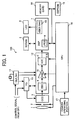
- Fig. 1 illustrates a digital camera 100 according to the present invention.
- This digital camera 100 is structured by having a lens 1 for condensing an optical image of an object, an aperture stop portion 2 for focusing a luminous flux condensed by the lens 1, a CCD (Charge Coupled Device) 3 for carrying out photoelectric conversion to the optical image passed through the lens 1 and the aperture stop portion 2, a CDS (Correlated Double Sampling) 4 for reducing a noise included in the CCD 3, an AGC (Automatic Gain Control) 15, an A/D converter (ADC) 5 for converting an analog signal outputted from the CCD 3 to a digital signal.
- a lens 1 for condensing an optical image of an object
- an aperture stop portion 2 for focusing a luminous flux condensed by the lens 1
- a CCD (Charge Coupled Device) 3 for carrying out photoelectric conversion to the optical image passed through the lens 1 and the aperture stop portion 2
- CDS Correlated Double Sampling
- AGC Automatic Gain Control
- the digital camera 100 is provided with a timing generator (TG) 13 for generating timing for the above mentioned CCD 3, CDS 4, AGC 15 and A/D converter 5, a digital signal processing circuit (DSP) 7 for carrying out image processing pursuant to a parameter of the image processing, a frame memory (SDRAM) 6 for recording imaged pixels and storing an image processed with the image processing, a displaying portion 8 for displaying an imaged image by a LCD (Liquid Crystal Display), an image compression and decompression circuit 9 for compressing image data processed by the digital signal processing circuit 7 or decompressing it to an original image data, a memory card 10 for storing the compressed image data compressed by the image compression and decompression circuit 9, a CPU 14 for executing a predetermined control based on a control program, a EEPROM (Electrically Erasable and Programmable Read Only Memory) 16 for storing a parameter, a camera operating portion 17 provided with a release button and the like for an user to operate a main body of the camera, and a CL
- the clock of the TG 13 is explained here that the clock of the TG 13 is structured to be generated by the CLK Gen 11 capable of outputting a variable frequency, to synchronize the DSP 7 with a system of the digital camera.
- a clock for peripheral devices such as an USB is also supplied to the DSP 7 from the CLK Gen 11 other than a clock for the system.
- This CLK Gen 11 has the multiplexer inside thereof, and can change the output frequency by the control of the CPU 14.
- the CPU 14 is structured to have functions to perform respective calculations such as AE, AF or white balance, to set parameters to the DSP 7 and to a F/E 12 (Front/End: signal processing of the CCD), and to process operations operated by the user.
- an integrated value of a luminance signal is obtained by the DSP 7 from a signal of the CCD 3 while monitoring is carried out, and an aperture stop and an electronic shutter are controlled by the CPU 14 by setting the obtained integrated value as an evaluation value.
- Evaluation values for the AF and the white balance and the like are also created by the DSP 7 other than the evaluation value for the AE, and are calculated by the CPU 14.
- the output signal outputted from the CCD 3 is converted from an analog to a digital by the A/D converter 5 via the CDS 4 and the AGC 15, and the converted digital signal is stored to the SDRAM 6 while keeping data pattern of the CCD 3.
- the luminance signal and a color signal are created by reading out data of the CCD 3 from the SDRAM 6, and the JPEG process is carried out thereto, and is recorded to the memory card 10.
- data converted from raw data of the CCD 3 to RGB or YUV which are for displaying is outputted from a Video DAC 18 provided inside of the DSP 7 and is displayed by the LCD 8.
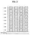
- Fig. 2 is a diagram showing an example of an inner structure of the CCD 3 which reads out 3 fields in a Bayer pattern.
- a first field 1(A) is arranged with pixels in order from R, Gr, R to Gr and so on in a first line
- a second field 2(B) is arranged with pixels in order from Gb, B, Gb, to B and so on in a second line
- a third field(C) is arranged with pixels in order from R, Gr, R to Gr and so on in a third line, and the arrangement is similarly repeated from then on.
- the arrangements of pixels in the first field 1(A) and the third field 3(C) are the same, they are arranged so as a two dimensional position becomes different.
- the CCD 3 for reading out 3 fields structures 1 frame by the fields from the first field to the third field.
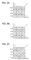
- Figs. 3A to 3C are diagrams showing output signals from each of the fields.
- Fig. 3A is a diagram showing the output signals from the first field, and shows that each of the signals of 1(A), 4(A), 7(A), 10(A) and so on in Fig. 2 are outputted.
- Fig. 3B shows the output signals from the second field, and shows that each of the signals of 2(B), 5(B), 8(B), 11(B) and so on in Fig. 2 are outputted.
- Fig. 3C is a diagram which shows the output signals from the third field, and shows that each of the signals of 3(C), 6(C), 9(C), 12(C) and so on in Fig. 2 are outputted.
- both the luminance signal and the color signal can be played.
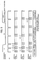
- Fig. 4 is a timing chart of a read out representing a normal operation of the CCD for reading out the 3 fields.
- a first line in Fig. 4 shows a wave pattern of an operation of a mechanical shutter, and "A" shown in the wave pattern represents that the shutter is open, and “B” represents that the shutter is shut.
- a second line shows a VD which represents an image data.
- Third to fifth lines represent vertical-drive pulses A-C respectively, and by setting center lines 0 V in respective wave patterns in each of the vertical-drive pulses A-C as a center, upper side of the center lines 0 V represents a "shift” pulse (+ V), and lower side of the center lines 0 V represents a "transfer” pulse (- V).
- operations carried out while in each timing are shown at the bottom line.
- each of the pixels in Fig. 2 is transferred to a register in order by means of the transfer pulse, and that pixels are shifted by means of the shift pulse when all the pixels which are in vertical are assembled. Also, the other fields are operated similarly.
- the mechanical shutter is opened by an operation of monitoring, and the image VD is sequentially transferred to the register by the vertical-drive pulses A-C, and the transferred image VD is shifted by shift pulses a1-c1.
- the shifted image VD is sequentially transferred to the register by the respective vertical-drive pulses A-C by the timing of "exposure" shown in the bottom line of Fig. 4 , and the mechanical shutter is shut, and the first field is outputted by a shift pulse a2. Subsequently, the second field is outputted by a shift pulse b2, and the third field is outputted by a shift pulse c2.
- Fig. 5 is a timing chart of a read out to show an operation for re-exposing the third field of the CCD which reads out the 3 fields.
- This operation outputs the third field after carrying out the re-exposure by opening the mechanical shutter again if the object is not moved at the time of outputting the third field.
- the mechanical shutter is opened by the operation of the monitoring, and the image VD is sequentially transferred to the register by the vertical-drive pulses A-C, and the transferred image VD is shifted by shift pulses a11-c11.
- the shifted image VD is sequentially transferred to the register by the respective vertical-drive pulses A-C by the timing of the "exposure”, and the mechanical shutter is closed, and the first field is outputted by a shift pulse a12.
- the second field is outputted by a shift pulse b12.
- the third field is outputted by a shift pulse c12 after carrying out the re-exposure by opening the mechanical shutter again.
- an image of the 1 frame is recorded to the memory.
- Fig. 6 is a flowchart of a read out showing the normal operation of the CCD 3 for reading out 3 fields of the present invention.
- the image in each of the fields is monitored by carrying out the monitoring (S1).
- the evaluation value of the AE is calculated from a result of the monitoring (S2), and if the result of the calculation shows that the image is not in the low luminance (S3/NO), data in each of the fields is read out by carrying out the exposure (S5), and the normal process for the still image is performed (S9). If the result of the calculation shows that the image is in the low luminance (S3/YES), the exposure and the read out of the field data in each of the fields are carried out (S4), and the first and second field data such as a difference of the luminance are compared (S6).
- the object may also be recommendable to add the entire field data from the first to the third field data in the step S8 by outputting the third field data after opening the mechanical shutter again and re-exposing the third field.
- step S7 it may also be recommendable that if the object is not moved in the step S7 (S7/NO), the entire field data from the first to the third field data are added in the step S8 by outputting the third field data after slowing down a frequency of the clock of the timing generator 13 as well as opening the mechanical shutter again and re-exposing the third field.
- Figs. 7A to 7C are pattern diagrams explaining the addition for adding pixels which are in the same color in the digital camera of the present invention.
- Fig. 7A represents a part of the pixels in the first field
- Fig. 7B represents a part of the pixels in the second field
- Fig. 7C represents a part of the pixels in the third field.
- pixels denoted by reference numeral 20 in the second field shown in Fig. 7B are discarded since they are in different colors.
- sensitivity can be enhanced approximately 3 times more than a conventional image of 1 frame structured by one field with the same exposure time.
- the present invention because the same colored pixels in the entire fields are added when the object is in the low luminance and is not moved, the present invention makes it possible to carry out the photographing in the low luminance without changing the exposure time, thus blurring by shaking can be avoided.
- the field data such as the difference of the luminance of images of the first field and the second field of the exposed image are compared at the time of the low luminance, and when it is determined that the there is no movement in the object, the same colored pixels of the entire fields are added after the re-exposing of the third field is carried out by opening the mechanical shutter again. Accordingly, the image in the third field becomes more distinct. Thereafter, by adding the same colored pixels in the entire fields, even more distinct images can be photographed.
- the image in the third field becomes more distinct by adding the same colored pixels in the entire fields after re-exposing the third field by opening the mechanical shutter again in the case the object is in the low luminance and has no movement, the blurring by the shaking can be avoided as well as more distinct photographing can be performed by making it possible to carry out the photographing in the low luminance without changing the exposure time.
- the frequency of the driving clock of the CCD is lowered as well as the same-colored pixels in the entire fields are added after re-exposing the third field by opening the mechanical shutter again in the case the object is in the low luminance and is not moved, the image in the third field becomes more distinct. Therefore, not only the blurring by the shaking can be avoided as well as more distinct photographing can be performed by making it possible to carry out the photographing in the low luminance without changing the exposure time, but also the power consumption in the entire imaging apparatus can be reduced.
- the size of the final files (normally in JPEG file) in both of them becomes small unless the interpolation process and the magnification process are carried out by the signal processing. Accordingly, it is necessary to carry out the above mentioned reading out of the 3 fields only when the file size having number of vertical pixels below 1/3 is selected.
- the present invention is further provided with means for carrying out the adding of pixels when the object is in the low luminance which is capable of selecting whether or not to carry out the adding of the same-colored pixels in each of the above mentioned fields.
Landscapes
- Engineering & Computer Science (AREA)
- Multimedia (AREA)
- Signal Processing (AREA)
- Physics & Mathematics (AREA)
- Spectroscopy & Molecular Physics (AREA)
- Computing Systems (AREA)
- Theoretical Computer Science (AREA)
- Color Television Image Signal Generators (AREA)
- Studio Devices (AREA)
- Transforming Light Signals Into Electric Signals (AREA)
Claims (5)
- Abbildungsvorrichtung, die umfasst:eine Farbbildaufnahmevorrichtung (3) zum Bilden eines Bildes eines Objektes in einem Rahmen aus jedem von mehreren Feldern und Aufweisen eines Ausgangs, der jedes der Felder getrennt ausgeben kann;eine Ansteuerungsschaltung (14) zum Ansteuern der Farbbildaufnahmevorrichtung (3) ;eine Zeitvorgabe-Erzeugungsschaltung (13) zum Erzeugen eines Ansteuerung, die die Farbbildaufnahmevorrichtung (3) zeitlich steuert; undeine Signalverarbeitungsvorrichtung (7) zum Verarbeiten eines Ausgangssignals der Farbbildaufnahmevorrichtung (3) durch Addieren von Datenwerten von entsprechenden Pixeln und Farben von jedem der Felder, wenn bestimmt wurde, dass sich das Objekt nicht bewegt hat, wenn durch Vergleichen der ausgegebenen Bilder bestimmt wurde, dass ein Unterschied zwischen der Helligkeit von benachbarten Feldern der Farbbildaufnahmevorrichtung kleiner als ein Grenzwert ist; gekennzeichnet durch:Mittel zum Berechnen eines Helligkeitswerts des Bildes; und dadurch, dass:die Signalverarbeitungsvorrichtung ausgelegt ist, das Addieren und die Bewegungsbestimmung auszuführen, wenn die berechnete Helligkeit gering ist, und das Addieren und die Bewegungsbestimmung nicht auszuführen, wenn der berechnete Helligkeitswert groß ist.
- Abbildungsvorrichtung nach Anspruch 1, wobei die Datenwerte von entsprechenden Pixeln nach dem Wiederbelichten eines nächsten Feldes, das das nächste von benachbarten Feldern der Farbbildaufnahmevorrichtung ist, addiert werden.
- Abbildungsvorrichtung nach Anspruch 2, die ferner einen variablen Takterzeuger (11) umfasst, der mehrere Taktfrequenzen für die Takterzeugungsschaltung (13) erzeugen kann; und wobei
die Datenwerte von entsprechenden Pixeln nach dem Senken einer Geschwindigkeit einer Taktfrequenz der Zeitvorgabe-Erzeugungsschaltung und Wiederbelichten des nächsten Feldes, das das nächste von benachbarten Feldern der Farbbildaufnahmevorrichtung ist, addiert werden. - Abbildungsvorrichtung nach Anspruch 1, 2 oder 3, dadurch gekennzeichnet, dass die Farbbildaufnahmevorrichtung (3) nur betreiben wird, wenn eine Größe einer Datei, die in einem Feld abgespielt werden kann, ausgewählt ist.
- Abbildungsvorrichtung nach Anspruch 1, 2, 3 oder 4, die ferner eine Vorrichtung zum Auswählen umfasst, ob Pixel zu einer Zeit von geringer Helligkeit zu addieren sind oder nicht, die fähig ist, auszuwählen, ob die Datenwerte von entsprechenden Pixeln addiert werden oder nicht.
Applications Claiming Priority (2)
| Application Number | Priority Date | Filing Date | Title |
|---|---|---|---|
| JP2003021152 | 2003-01-29 | ||
| JP2003021152A JP4022152B2 (ja) | 2003-01-29 | 2003-01-29 | 撮像装置 |
Publications (3)
| Publication Number | Publication Date |
|---|---|
| EP1453308A2 EP1453308A2 (de) | 2004-09-01 |
| EP1453308A3 EP1453308A3 (de) | 2009-10-14 |
| EP1453308B1 true EP1453308B1 (de) | 2013-08-07 |
Family
ID=32767535
Family Applications (1)
| Application Number | Title | Priority Date | Filing Date |
|---|---|---|---|
| EP04250371.4A Expired - Lifetime EP1453308B1 (de) | 2003-01-29 | 2004-01-23 | Abbildungsvorrichtung |
Country Status (3)
| Country | Link |
|---|---|
| US (1) | US7345704B2 (de) |
| EP (1) | EP1453308B1 (de) |
| JP (1) | JP4022152B2 (de) |
Families Citing this family (7)
| Publication number | Priority date | Publication date | Assignee | Title |
|---|---|---|---|---|
| JP2006157568A (ja) * | 2004-11-30 | 2006-06-15 | Konica Minolta Holdings Inc | 撮像装置およびプログラム |
| US7710458B2 (en) * | 2005-06-17 | 2010-05-04 | Casio Computer Co., Ltd. | Image pick-up apparatus with a shake reducing function |
| US8169484B2 (en) * | 2005-07-05 | 2012-05-01 | Shai Silberstein | Photography-specific digital camera apparatus and methods useful in conjunction therewith |
| JP4976049B2 (ja) * | 2006-05-02 | 2012-07-18 | 株式会社リコー | 撮像装置 |
| JP5019543B2 (ja) | 2006-05-09 | 2012-09-05 | シャープ株式会社 | 撮像装置 |
| KR101571334B1 (ko) * | 2009-02-12 | 2015-11-24 | 삼성전자주식회사 | 디지털 영상 처리장치 및 그 제어방법 |
| US12301731B2 (en) * | 2019-06-28 | 2025-05-13 | Zebra Technologies Corporation | Methods and apparatus to renew digital certificates |
Citations (1)
| Publication number | Priority date | Publication date | Assignee | Title |
|---|---|---|---|---|
| JP2000224470A (ja) * | 1999-02-02 | 2000-08-11 | Minolta Co Ltd | カメラシステム |
Family Cites Families (17)
| Publication number | Priority date | Publication date | Assignee | Title |
|---|---|---|---|---|
| JP3560622B2 (ja) * | 1992-04-30 | 2004-09-02 | オリンパス株式会社 | 撮像装置 |
| JPH07284011A (ja) | 1994-04-05 | 1995-10-27 | Ricoh Co Ltd | デジタル電子スチルカメラ |
| JPH08289287A (ja) | 1995-04-12 | 1996-11-01 | Ricoh Co Ltd | 音声信号・映像信号処理装置 |
| JP3802596B2 (ja) * | 1995-12-07 | 2006-07-26 | オリンパス株式会社 | 電子カメラ |
| JP3745067B2 (ja) * | 1996-02-20 | 2006-02-15 | キヤノン株式会社 | 撮像装置及びその制御方法 |
| JPH09322191A (ja) | 1996-03-29 | 1997-12-12 | Ricoh Co Ltd | 画像入力装置 |
| JP3440722B2 (ja) * | 1996-09-20 | 2003-08-25 | ソニー株式会社 | 固体撮像装置およびその駆動方法並びにカメラ |
| JP4161384B2 (ja) * | 1997-04-30 | 2008-10-08 | ソニー株式会社 | 固体撮像装置、これを用いたカメラおよび固体撮像装置の駆動方法 |
| JPH1141515A (ja) * | 1997-07-24 | 1999-02-12 | Minolta Co Ltd | スチルカメラ |
| JP4078741B2 (ja) * | 1999-01-07 | 2008-04-23 | ソニー株式会社 | 固体撮像装置およびその駆動方法並びにカメラシステム |
| JP2001145025A (ja) * | 1999-11-12 | 2001-05-25 | Nec Corp | 固体撮像装置およびその駆動方法 |
| US6532264B1 (en) * | 2000-03-27 | 2003-03-11 | Teranex, Inc. | Processing sequential video images to detect image motion among interlaced video fields or progressive video images |
| JP3854826B2 (ja) * | 2001-08-08 | 2006-12-06 | キヤノン株式会社 | 撮像装置 |
| JP3682482B2 (ja) * | 2002-04-24 | 2005-08-10 | コニカミノルタフォトイメージング株式会社 | 撮像装置 |
| US7710458B2 (en) * | 2005-06-17 | 2010-05-04 | Casio Computer Co., Ltd. | Image pick-up apparatus with a shake reducing function |
| JP4619895B2 (ja) * | 2005-08-12 | 2011-01-26 | 富士フイルム株式会社 | 撮像装置、画像処理装置、撮像方法、及び画像処理方法 |
| JP4357471B2 (ja) * | 2005-09-30 | 2009-11-04 | 三洋電機株式会社 | 画像取得装置及びプログラム |
-
2003
- 2003-01-29 JP JP2003021152A patent/JP4022152B2/ja not_active Expired - Fee Related
-
2004
- 2004-01-22 US US10/761,329 patent/US7345704B2/en not_active Expired - Fee Related
- 2004-01-23 EP EP04250371.4A patent/EP1453308B1/de not_active Expired - Lifetime
Patent Citations (1)
| Publication number | Priority date | Publication date | Assignee | Title |
|---|---|---|---|---|
| JP2000224470A (ja) * | 1999-02-02 | 2000-08-11 | Minolta Co Ltd | カメラシステム |
Also Published As
| Publication number | Publication date |
|---|---|
| EP1453308A2 (de) | 2004-09-01 |
| US20050078201A1 (en) | 2005-04-14 |
| JP2004235901A (ja) | 2004-08-19 |
| US7345704B2 (en) | 2008-03-18 |
| EP1453308A3 (de) | 2009-10-14 |
| JP4022152B2 (ja) | 2007-12-12 |
Similar Documents
| Publication | Publication Date | Title |
|---|---|---|
| KR100819804B1 (ko) | 촬상 장치 | |
| JP5112104B2 (ja) | 画像処理装置及び画像処理プログラム | |
| KR101247647B1 (ko) | 화상 합성 장치, 화상 합성 방법, 및 기록 매체 | |
| JP4008778B2 (ja) | 撮像装置 | |
| KR101303410B1 (ko) | 촬상장치 및 촬상방법 | |
| US8305465B2 (en) | Image pick-up apparatus with a shake reducing function | |
| CN103491310B (zh) | 图像捕获装置及其控制方法 | |
| CN106797434A (zh) | 摄像装置、摄像方法、处理程序 | |
| JP2001211362A (ja) | デジタルカメラの構図補助フレーム選択方法及びデジタルカメラ | |
| CN106358030A (zh) | 图像处理装置和图像处理方法 | |
| JP5009880B2 (ja) | 撮像装置及び撮像方法 | |
| EP2214136B1 (de) | Verfahren und Programm zur Steuerung der Bildaufnahmevorrichtung | |
| JP2010093679A (ja) | 撮像装置及び撮像制御方法 | |
| EP3249906A1 (de) | Bildaufnahmevorrichtung, bildaufnahmeverfahren und bildanzeigevorrichtung | |
| JP4738907B2 (ja) | 固体撮像素子および固体撮像装置 | |
| EP1453308B1 (de) | Abbildungsvorrichtung | |
| JP5002931B2 (ja) | 撮像装置及びそのプログラム | |
| JP2009164859A (ja) | 撮像装置及び撮像制御方法 | |
| JP2002232751A (ja) | 表示装置、表示方法、及び電子カメラ | |
| JP2010283504A (ja) | 撮像装置、撮像方法、および、撮像プログラム | |
| KR101612853B1 (ko) | 촬영장치, 촬영장치의 제어방법 및 제어방법을 실행시키기 위한 프로그램을 저장한 기록매체 | |
| JPH1169226A (ja) | 電子カメラ | |
| JP3563508B2 (ja) | 自動焦点調節装置 | |
| JP2004023745A (ja) | デジタルカメラ | |
| JP2012065125A (ja) | 撮像装置、電子機器、画像処理システムおよびコンピュータ読み取り可能な記録媒体 |
Legal Events
| Date | Code | Title | Description |
|---|---|---|---|
| PUAI | Public reference made under article 153(3) epc to a published international application that has entered the european phase |
Free format text: ORIGINAL CODE: 0009012 |
|
| 17P | Request for examination filed |
Effective date: 20040131 |
|
| AK | Designated contracting states |
Kind code of ref document: A2 Designated state(s): AT BE BG CH CY CZ DE DK EE ES FI FR GB GR HU IE IT LI LU MC NL PT RO SE SI SK TR |
|
| AX | Request for extension of the european patent |
Extension state: AL LT LV MK |
|
| PUAL | Search report despatched |
Free format text: ORIGINAL CODE: 0009013 |
|
| AK | Designated contracting states |
Kind code of ref document: A3 Designated state(s): AT BE BG CH CY CZ DE DK EE ES FI FR GB GR HU IE IT LI LU MC NL PT RO SE SI SK TR |
|
| AX | Request for extension of the european patent |
Extension state: AL LT LV MK |
|
| AKX | Designation fees paid |
Designated state(s): DE ES FR GB IT NL |
|
| 17Q | First examination report despatched |
Effective date: 20100609 |
|
| REG | Reference to a national code |
Ref country code: DE Ref legal event code: R079 Ref document number: 602004042959 Country of ref document: DE Free format text: PREVIOUS MAIN CLASS: H04N0005235000 Ipc: H04N0005232000 |
|
| GRAP | Despatch of communication of intention to grant a patent |
Free format text: ORIGINAL CODE: EPIDOSNIGR1 |
|
| RIC1 | Information provided on ipc code assigned before grant |
Ipc: H04N 5/235 20060101ALI20130204BHEP Ipc: H04N 9/04 20060101ALI20130204BHEP Ipc: H04N 5/232 20060101AFI20130204BHEP |
|
| GRAS | Grant fee paid |
Free format text: ORIGINAL CODE: EPIDOSNIGR3 |
|
| GRAA | (expected) grant |
Free format text: ORIGINAL CODE: 0009210 |
|
| AK | Designated contracting states |
Kind code of ref document: B1 Designated state(s): DE ES FR GB IT NL |
|
| REG | Reference to a national code |
Ref country code: GB Ref legal event code: FG4D |
|
| REG | Reference to a national code |
Ref country code: DE Ref legal event code: R096 Ref document number: 602004042959 Country of ref document: DE Effective date: 20131002 |
|
| REG | Reference to a national code |
Ref country code: NL Ref legal event code: VDEP Effective date: 20130807 |
|
| PG25 | Lapsed in a contracting state [announced via postgrant information from national office to epo] |
Ref country code: NL Free format text: LAPSE BECAUSE OF FAILURE TO SUBMIT A TRANSLATION OF THE DESCRIPTION OR TO PAY THE FEE WITHIN THE PRESCRIBED TIME-LIMIT Effective date: 20130807 |
|
| PG25 | Lapsed in a contracting state [announced via postgrant information from national office to epo] |
Ref country code: ES Free format text: LAPSE BECAUSE OF FAILURE TO SUBMIT A TRANSLATION OF THE DESCRIPTION OR TO PAY THE FEE WITHIN THE PRESCRIBED TIME-LIMIT Effective date: 20130807 Ref country code: IT Free format text: LAPSE BECAUSE OF FAILURE TO SUBMIT A TRANSLATION OF THE DESCRIPTION OR TO PAY THE FEE WITHIN THE PRESCRIBED TIME-LIMIT Effective date: 20130807 |
|
| PLBE | No opposition filed within time limit |
Free format text: ORIGINAL CODE: 0009261 |
|
| STAA | Information on the status of an ep patent application or granted ep patent |
Free format text: STATUS: NO OPPOSITION FILED WITHIN TIME LIMIT |
|
| 26N | No opposition filed |
Effective date: 20140508 |
|
| REG | Reference to a national code |
Ref country code: DE Ref legal event code: R097 Ref document number: 602004042959 Country of ref document: DE Effective date: 20140508 |
|
| REG | Reference to a national code |
Ref country code: FR Ref legal event code: PLFP Year of fee payment: 13 |
|
| REG | Reference to a national code |
Ref country code: FR Ref legal event code: PLFP Year of fee payment: 14 |
|
| PGFP | Annual fee paid to national office [announced via postgrant information from national office to epo] |
Ref country code: DE Payment date: 20170120 Year of fee payment: 14 Ref country code: FR Payment date: 20170120 Year of fee payment: 14 |
|
| PGFP | Annual fee paid to national office [announced via postgrant information from national office to epo] |
Ref country code: GB Payment date: 20170119 Year of fee payment: 14 |
|
| REG | Reference to a national code |
Ref country code: DE Ref legal event code: R119 Ref document number: 602004042959 Country of ref document: DE |
|
| GBPC | Gb: european patent ceased through non-payment of renewal fee |
Effective date: 20180123 |
|
| PG25 | Lapsed in a contracting state [announced via postgrant information from national office to epo] |
Ref country code: DE Free format text: LAPSE BECAUSE OF NON-PAYMENT OF DUE FEES Effective date: 20180801 Ref country code: FR Free format text: LAPSE BECAUSE OF NON-PAYMENT OF DUE FEES Effective date: 20180131 |
|
| REG | Reference to a national code |
Ref country code: FR Ref legal event code: ST Effective date: 20180928 |
|
| PG25 | Lapsed in a contracting state [announced via postgrant information from national office to epo] |
Ref country code: GB Free format text: LAPSE BECAUSE OF NON-PAYMENT OF DUE FEES Effective date: 20180123 |