EP1444379B1 - Atomic layer deposition apparatus and process - Google Patents
Atomic layer deposition apparatus and process Download PDFInfo
- Publication number
- EP1444379B1 EP1444379B1 EP02801694A EP02801694A EP1444379B1 EP 1444379 B1 EP1444379 B1 EP 1444379B1 EP 02801694 A EP02801694 A EP 02801694A EP 02801694 A EP02801694 A EP 02801694A EP 1444379 B1 EP1444379 B1 EP 1444379B1
- Authority
- EP
- European Patent Office
- Prior art keywords
- exhaust
- fore
- line
- coupled
- dispensing
- Prior art date
- Legal status (The legal status is an assumption and is not a legal conclusion. Google has not performed a legal analysis and makes no representation as to the accuracy of the status listed.)
- Expired - Lifetime
Links
Images
Classifications
-
- C—CHEMISTRY; METALLURGY
- C23—COATING METALLIC MATERIAL; COATING MATERIAL WITH METALLIC MATERIAL; CHEMICAL SURFACE TREATMENT; DIFFUSION TREATMENT OF METALLIC MATERIAL; COATING BY VACUUM EVAPORATION, BY SPUTTERING, BY ION IMPLANTATION OR BY CHEMICAL VAPOUR DEPOSITION, IN GENERAL; INHIBITING CORROSION OF METALLIC MATERIAL OR INCRUSTATION IN GENERAL
- C23C—COATING METALLIC MATERIAL; COATING MATERIAL WITH METALLIC MATERIAL; SURFACE TREATMENT OF METALLIC MATERIAL BY DIFFUSION INTO THE SURFACE, BY CHEMICAL CONVERSION OR SUBSTITUTION; COATING BY VACUUM EVAPORATION, BY SPUTTERING, BY ION IMPLANTATION OR BY CHEMICAL VAPOUR DEPOSITION, IN GENERAL
- C23C16/00—Chemical coating by decomposition of gaseous compounds, without leaving reaction products of surface material in the coating, i.e. chemical vapour deposition [CVD] processes
- C23C16/44—Chemical coating by decomposition of gaseous compounds, without leaving reaction products of surface material in the coating, i.e. chemical vapour deposition [CVD] processes characterised by the method of coating
- C23C16/4401—Means for minimising impurities, e.g. dust, moisture or residual gas, in the reaction chamber
-
- C—CHEMISTRY; METALLURGY
- C23—COATING METALLIC MATERIAL; COATING MATERIAL WITH METALLIC MATERIAL; CHEMICAL SURFACE TREATMENT; DIFFUSION TREATMENT OF METALLIC MATERIAL; COATING BY VACUUM EVAPORATION, BY SPUTTERING, BY ION IMPLANTATION OR BY CHEMICAL VAPOUR DEPOSITION, IN GENERAL; INHIBITING CORROSION OF METALLIC MATERIAL OR INCRUSTATION IN GENERAL
- C23C—COATING METALLIC MATERIAL; COATING MATERIAL WITH METALLIC MATERIAL; SURFACE TREATMENT OF METALLIC MATERIAL BY DIFFUSION INTO THE SURFACE, BY CHEMICAL CONVERSION OR SUBSTITUTION; COATING BY VACUUM EVAPORATION, BY SPUTTERING, BY ION IMPLANTATION OR BY CHEMICAL VAPOUR DEPOSITION, IN GENERAL
- C23C16/00—Chemical coating by decomposition of gaseous compounds, without leaving reaction products of surface material in the coating, i.e. chemical vapour deposition [CVD] processes
- C23C16/44—Chemical coating by decomposition of gaseous compounds, without leaving reaction products of surface material in the coating, i.e. chemical vapour deposition [CVD] processes characterised by the method of coating
- C23C16/4412—Details relating to the exhausts, e.g. pumps, filters, scrubbers, particle traps
-
- C—CHEMISTRY; METALLURGY
- C23—COATING METALLIC MATERIAL; COATING MATERIAL WITH METALLIC MATERIAL; CHEMICAL SURFACE TREATMENT; DIFFUSION TREATMENT OF METALLIC MATERIAL; COATING BY VACUUM EVAPORATION, BY SPUTTERING, BY ION IMPLANTATION OR BY CHEMICAL VAPOUR DEPOSITION, IN GENERAL; INHIBITING CORROSION OF METALLIC MATERIAL OR INCRUSTATION IN GENERAL
- C23C—COATING METALLIC MATERIAL; COATING MATERIAL WITH METALLIC MATERIAL; SURFACE TREATMENT OF METALLIC MATERIAL BY DIFFUSION INTO THE SURFACE, BY CHEMICAL CONVERSION OR SUBSTITUTION; COATING BY VACUUM EVAPORATION, BY SPUTTERING, BY ION IMPLANTATION OR BY CHEMICAL VAPOUR DEPOSITION, IN GENERAL
- C23C16/00—Chemical coating by decomposition of gaseous compounds, without leaving reaction products of surface material in the coating, i.e. chemical vapour deposition [CVD] processes
- C23C16/44—Chemical coating by decomposition of gaseous compounds, without leaving reaction products of surface material in the coating, i.e. chemical vapour deposition [CVD] processes characterised by the method of coating
- C23C16/455—Chemical coating by decomposition of gaseous compounds, without leaving reaction products of surface material in the coating, i.e. chemical vapour deposition [CVD] processes characterised by the method of coating characterised by the method used for introducing gases into reaction chamber or for modifying gas flows in reaction chamber
- C23C16/45523—Pulsed gas flow or change of composition over time
- C23C16/45525—Atomic layer deposition [ALD]
- C23C16/45544—Atomic layer deposition [ALD] characterized by the apparatus
-
- C—CHEMISTRY; METALLURGY
- C23—COATING METALLIC MATERIAL; COATING MATERIAL WITH METALLIC MATERIAL; CHEMICAL SURFACE TREATMENT; DIFFUSION TREATMENT OF METALLIC MATERIAL; COATING BY VACUUM EVAPORATION, BY SPUTTERING, BY ION IMPLANTATION OR BY CHEMICAL VAPOUR DEPOSITION, IN GENERAL; INHIBITING CORROSION OF METALLIC MATERIAL OR INCRUSTATION IN GENERAL
- C23C—COATING METALLIC MATERIAL; COATING MATERIAL WITH METALLIC MATERIAL; SURFACE TREATMENT OF METALLIC MATERIAL BY DIFFUSION INTO THE SURFACE, BY CHEMICAL CONVERSION OR SUBSTITUTION; COATING BY VACUUM EVAPORATION, BY SPUTTERING, BY ION IMPLANTATION OR BY CHEMICAL VAPOUR DEPOSITION, IN GENERAL
- C23C16/00—Chemical coating by decomposition of gaseous compounds, without leaving reaction products of surface material in the coating, i.e. chemical vapour deposition [CVD] processes
- C23C16/44—Chemical coating by decomposition of gaseous compounds, without leaving reaction products of surface material in the coating, i.e. chemical vapour deposition [CVD] processes characterised by the method of coating
- C23C16/455—Chemical coating by decomposition of gaseous compounds, without leaving reaction products of surface material in the coating, i.e. chemical vapour deposition [CVD] processes characterised by the method of coating characterised by the method used for introducing gases into reaction chamber or for modifying gas flows in reaction chamber
- C23C16/45587—Mechanical means for changing the gas flow
Definitions
- the present invention relates to atomic layer deposition. More specifically, the present invention relates to an apparatus and process for improving the performance of an atomic layer deposition chamber.
- a method of depositing very thin films is atomic layer deposition (ALD). This method has several advantages over tradition chemical vapor deposition. It can be performed at lower temperatures, uses a wide range of precursors, produces very thin films, inherently obtains 100% step coverage, and can be used to "microengineer" complex film matrices.
- ALD ALD
- individual precursors are pulsed onto the surface of a wafer in a sequential manner, without mixing the precursors in the gas phase.
- Each individual precursor reacts with the surface to form an atomic layer in a way that only one layer can form at a time.
- the surface reaction occurs such that the reaction is complete, and permits no more than one layer at a time to be deposited. This occurs no matter how many molecules are applied to the surface in an overdosing mode.
- the films are built up by introducing short bursts of gases in rapid cycles.
- ALD ALD method
- One problem concerns the diversion of the flow of liquid precursors introduced in a vapor phase.
- the flow In order to keep the flow active, the flow must be diverted to a fore-line of the ALD chamber when the liquid precursor is not needed in the deposition process.
- the opposing gas is pulsed, the unreacted chemical is mixed in the fore-line with the diverted chemical and reacts causing a build up in the fore-line. The build up can be severe and clogs the fore-line.
- a second problem concerns the reaction of the gases. Process gases are introduced individually for the ALD process and disposed of through the same fore lines causing the gases or vapors to react with one another.
- the present invention fulfills the first need of minimizing clogging of the fore-line by providing an ALD apparatus and process that allows separate chemicals to only mix when and where desired by installing and monitoring a second fore-line.
- the present invention fulfills the second need of minimizing the reaction of the gases in the pump lines, by allowing the reactive gases or vapors to be removed from the process reactor chamber without coming in contact with one another in an area that would create an unwanted reaction of the process gases or vapors. This is accomplished by providing independent and dedicated pumping lines and corresponding isolation valves that are activated for the specific gas when needed.
- the separate pump lines allow the gas to be exhausted in a manner that minimizes possible unwanted reaction of the reactive gases. Accordingly, it is an object of the present invention to provide an improved ALD apparatus and process using dispensing fore-lines and a second exhaust path in order to prevent clogging of the exhaust fore-line.
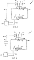
- FIG. 1 illustrates an ALD apparatus 2 comprising a process reactor chamber 10 , a first dispensing valve 4 , a second dispensing value 8 , an isolation valve 24 , an exhaust fore-line 22 , an exhaust pump 20 , and a dispensing fore-line 26 .
- the process reactor chamber 10 includes a first precursor inlet 14 , a second precursor inlet 16 , and a first chamber outlet 17 .
- the first dispensing valve 4 is coupled to the first precursor inlet 14 of the process reactor chamber 10 .
- the second dispensing valve 8 is coupled to the second precursor inlet 16 of said process reactor chamber 10 .
- the isolation valve 24 is directly coupled to the first chamber outlet 17 of the process reactor chamber 10 .
- the exhaust pump 20 is coupled to the isolation valve 24 by the exhaust fore-line 22 , defining an exhaust path.
- the dispensing fore-line 26 comprises a first end 25 and a second end 27 .
- the first end 25 is coupled to the first dispensing valve 4 and the second end 27 is coupled to the exhaust pump 20 .
- no substantial exhaust fore-line exists between the isolation valve 24 and the first chamber outlet 17 because, as is noted above, the isolation valve 24 is directly coupled to the outlet 17 .
- the first dispensing valve 4 allows a first precursor 6 to flow into the process reactor chamber 10 through a first precursor inlet 14 .
- a continuous flow of the first precursor 6 must be maintained. Therefore, the first dispensing valve 4 selectively diverts the direction of the first precursor 6 to the first precursor inlet 14 of the process reactor chamber 10 .
- the first precursor 6 is not diverted into the process reactor chamber 10 , it is sent to the exhaust pump 20 via a dispensing fore-line 26 .
- the dispensing fore-line 26 is used to discard the first precursor 6 when it is not diverted into the first precursor inlet 14 .
- the dispensing fore-line 26 may be used to isolate the first precursor 6 from other chemicals, precursors, and exhausts that would otherwise mix with the first precursor 6 and potentially cause clogging of the first exhaust fore-line 22 .
- the exhaust fore-line 22 remains clean and flow remains stable and consistent.
- the process reactor chamber 10 comprises a first precursor inlet 14 , a second precursor inlet 16 , a heater 13 , a wafer 11 , and a shower head device 18 .
- the first precursor inlet 14 and second precursor inlet 16 can share a common opening 12 or alternatively have separate openings.
- the first precursor inlet 14 may direct the first precursor 6 through a shower head device 18 that distributes the first precursor 6 into the process reactor chamber 10 .
- the first precursor 6 is absorbed onto the surface of a wafer 11 .
- the wafer rests on a heater 13 .
- the manner in which absorption of the precursor is achieved is beyond the scope of the present invention and is well known in the art. It may be gleaned from any one of a number of teachings relating to atomic layer deposition.
- unreacted first precursor is purged out of the process reactor chamber 10 by introducing a purge gas via the purge valve 7 into the chamber outlet 17 . Unreacted first precursor flows directly into the isolation valve 24 where unreacted first precursor is transferred to the exhaust pump 20 via the exhaust fore-line 22 .
- the first precursor 6 and second precursor 9 are introduced in separate intervals. Once unreacted first precursor is purged from the process reactor chamber 10 through use of the purging valve 7 , the second dispensing valve 8 allows for the introduction of the second precursor 9 into the second precursor inlet 16 and ultimately into the process reactor chamber 10 .
- the second precursor inlet 16 directs the second precursor 9 through a shower head device 18 that distributes the second precursor 9 into the process reactor chamber 10 .
- the second precursor 9 then reacts with the layer formed on the wafer 11 from the first precursor 6 , creating a monolayer of film on the wafer 11 .
- Unreacted second precursor is purged from the process reactor chamber 10 , using the purging valve 7 , into the chamber outlet 17 . Unreacted second precursor flows directly into the isolation valve 24 where unreacted second precursor is transferred to the exhaust pump 20 via the exhaust fore-line 22 .
- This process of the introduction, reaction, and purging alternating the first precursor 6 with the second precursor 9 is performed at a high rate of speed with continuous successions.
- the embodiment of the present invention illustrated in Fig. 2 differs from Fig.1 in that it utilizes a dispensing pump 28 .
- the first end 25 of the dispensing fore-line 26 is coupled to the dispensing valve 4 .
- the second end 27 of the dispensing fore-line 26 is coupled to the dispensing pump 28 .
- the dispensing pump 28 collects the undiverted first precursor 6 so that the undiverted first precursor 6 is isolated from other chemicals, precursors, and exhausts that would otherwise mix with the first precursor 6 and potentially cause clogging of the first exhaust fore-line 22 .
- the exhaust fore-line 22 remains clean and flow remains stable and consistent.
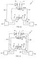
- Fig. 3 differs from that illustrated in Fig. 2 because the second isolation valve 34 , the second exhaust fore-line 36 , and the second exhaust pump 30 are shown, thus defining a second exhaust path.
- This second exhaust path is constructed to keep the unreacted first precursor and the unreacted second precursor separate. Thereby, reducing the possibility of mixing and clogging the either of the exhaust fore-lines 22, 36 .
- the second isolation valve 34 , the second exhaust fore-line 36 , and the second exhaust pump 30 operate in a similar manner as the-first isolation valve 24 , the first exhaust fore-line 22 , and the first exhaust pump 20 .
- the unreacted second precursor is purged out of the process reactor chamber 10 by introducing a purge gas via the purge valve 7 into the second chamber outlet 29 .
- the unreacted second precursor flows directly into the second isolation valve 34 where the unreacted second precursor is transferred to the second exhaust pump 30 via the second exhaust fore-line 36 .
- the embodiment in Fig. 3 also differs from that illustrated in Fig. 2 because the dispensing fore-line 26 is connected to the first exhaust path. Specifically, the dispensing fore-line 26 is connected to the first exhaust pump 20 .
- the dispensing valve could alternatively be coupled to the first exhaust fore-line 22 or directly to a dispensing pump 28 as illustrated in Fig. 2.
- the embodiment of Fig. 4 differs from that of Fig. 3 because a second dispensing fore-line 36 is extended from the second dispensing valve 8 to the second exhaust path, specifically the second exhaust fore-line 33 .
- the second dispensing fore-line 36 can alternatively be directly connected to the second exhaust pump 30 , similar to the embodiment of Fig. 1 or connected to a second dispensing pump, similar to the embodiment of Fig. 2.
- the second dispensing pump would operate in a similar manner as the first dispensing pump 28 described above.
- the second dispensing pump collects the undiverted second precursor 9 so that the undiverted second precursor 9 is isolated from other chemicals, precursors, and exhausts that would otherwise mix with the second precursor 9 and potentially cause clogging of the second exhaust fore-line 36 .
- the second exhaust fore-line 36 remains clean and flow remains stable and consistent.
- the second dispensing fore-line 36 operates in a similar manner as the first dispensing fore-line 26 .
- the second dispensing fore-line 36 is used to discard the second precursor 9 when it is not diverted into the second precursor inlet 16 .
- the second dispensing fore-line 36 may be used to isolate the second precursor 9 from other chemicals, precursors, and exhausts that would otherwise mix with the second precursor 9 and potentially cause clogging of the second exhaust fore-line 33 .
- the second exhaust fore-line 33 remains clean and flow remains stable and consistent.
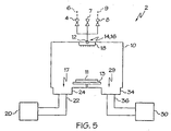
- Fig. 5 differs from the previous figures because it does not show the first dispensing fore-line 26 or the second dispensing fore-line 36 . Therefore, only the two separate exhaust paths are depicted.
Landscapes
- Chemical & Material Sciences (AREA)
- General Chemical & Material Sciences (AREA)
- Chemical Kinetics & Catalysis (AREA)
- Engineering & Computer Science (AREA)
- Materials Engineering (AREA)
- Mechanical Engineering (AREA)
- Metallurgy (AREA)
- Organic Chemistry (AREA)
- Chemical Vapour Deposition (AREA)
Applications Claiming Priority (7)
| Application Number | Priority Date | Filing Date | Title |
|---|---|---|---|
| US977612 | 2001-10-15 | ||
| US09/977,612 US6461436B1 (en) | 2001-10-15 | 2001-10-15 | Apparatus and process of improving atomic layer deposition chamber performance |
| US166902 | 2002-06-11 | ||
| US10/166,902 US6716284B2 (en) | 2001-10-15 | 2002-06-11 | Apparatus and process of improving atomic layer deposition chamber performance |
| US10/190,792 US6758911B2 (en) | 2001-10-15 | 2002-07-08 | Apparatus and process of improving atomic layer deposition chamber performance |
| US190792 | 2002-07-08 | ||
| PCT/US2002/032741 WO2003033762A1 (en) | 2001-10-15 | 2002-10-15 | Atomic layer deposition apparatus and process |
Publications (2)
| Publication Number | Publication Date |
|---|---|
| EP1444379A1 EP1444379A1 (en) | 2004-08-11 |
| EP1444379B1 true EP1444379B1 (en) | 2005-05-04 |
Family
ID=27389326
Family Applications (1)
| Application Number | Title | Priority Date | Filing Date |
|---|---|---|---|
| EP02801694A Expired - Lifetime EP1444379B1 (en) | 2001-10-15 | 2002-10-15 | Atomic layer deposition apparatus and process |
Country Status (6)
| Country | Link |
|---|---|
| EP (1) | EP1444379B1 (ja) |
| JP (1) | JP2005506446A (ja) |
| KR (1) | KR100683441B1 (ja) |
| CN (1) | CN1306062C (ja) |
| DE (1) | DE60204043T2 (ja) |
| WO (1) | WO2003033762A1 (ja) |
Families Citing this family (21)
| Publication number | Priority date | Publication date | Assignee | Title |
|---|---|---|---|---|
| US6461436B1 (en) | 2001-10-15 | 2002-10-08 | Micron Technology, Inc. | Apparatus and process of improving atomic layer deposition chamber performance |
| US6861094B2 (en) | 2002-04-25 | 2005-03-01 | Micron Technology, Inc. | Methods for forming thin layers of materials on micro-device workpieces |
| US6838114B2 (en) | 2002-05-24 | 2005-01-04 | Micron Technology, Inc. | Methods for controlling gas pulsing in processes for depositing materials onto micro-device workpieces |
| US7118783B2 (en) | 2002-06-26 | 2006-10-10 | Micron Technology, Inc. | Methods and apparatus for vapor processing of micro-device workpieces |
| US6821347B2 (en) | 2002-07-08 | 2004-11-23 | Micron Technology, Inc. | Apparatus and method for depositing materials onto microelectronic workpieces |
| JP4113755B2 (ja) * | 2002-10-03 | 2008-07-09 | 東京エレクトロン株式会社 | 処理装置 |
| JP4423914B2 (ja) | 2003-05-13 | 2010-03-03 | 東京エレクトロン株式会社 | 処理装置及びその使用方法 |
| GB0322602D0 (en) * | 2003-09-26 | 2003-10-29 | Boc Group Inc | Vent-run gas switching systems |
| US7258892B2 (en) | 2003-12-10 | 2007-08-21 | Micron Technology, Inc. | Methods and systems for controlling temperature during microfeature workpiece processing, e.g., CVD deposition |
| US20050145181A1 (en) * | 2003-12-31 | 2005-07-07 | Dickinson Colin J. | Method and apparatus for high speed atomic layer deposition |
| US7906393B2 (en) | 2004-01-28 | 2011-03-15 | Micron Technology, Inc. | Methods for forming small-scale capacitor structures |
| US8133554B2 (en) | 2004-05-06 | 2012-03-13 | Micron Technology, Inc. | Methods for depositing material onto microfeature workpieces in reaction chambers and systems for depositing materials onto microfeature workpieces |
| US8435351B2 (en) * | 2004-11-29 | 2013-05-07 | Tokyo Electron Limited | Method and system for measuring a flow rate in a solid precursor delivery system |
| KR101272321B1 (ko) * | 2005-05-09 | 2013-06-07 | 한국에이에스엠지니텍 주식회사 | 복수의 기체 유입구를 가지는 원자층 증착 장치의 반응기 |
| US7562672B2 (en) * | 2006-03-30 | 2009-07-21 | Applied Materials, Inc. | Chemical delivery apparatus for CVD or ALD |
| JP6167673B2 (ja) | 2013-05-31 | 2017-07-26 | 東京エレクトロン株式会社 | 成膜装置、成膜方法及び記憶媒体 |
| KR102181122B1 (ko) | 2016-12-13 | 2020-11-20 | 주식회사 원익아이피에스 | 기판 처리 장치 및 이를 이용한 기판 처리 방법 |
| CN109402608B (zh) * | 2017-08-16 | 2020-12-08 | 北京北方华创微电子装备有限公司 | 一种原子层沉积设备的气路系统及其控制方法 |
| CN109750274B (zh) * | 2017-11-01 | 2021-10-22 | 长鑫存储技术有限公司 | 半导体生产设备及半导体工艺方法 |
| CN107988587B (zh) * | 2017-11-14 | 2020-04-24 | 沈阳拓荆科技有限公司 | 一种气体分流合流装置 |
| CN110055515A (zh) * | 2018-01-18 | 2019-07-26 | 北京北方华创微电子装备有限公司 | 一种原子层沉积设备的气路系统及其控制方法 |
Family Cites Families (9)
| Publication number | Priority date | Publication date | Assignee | Title |
|---|---|---|---|---|
| JPH01189114A (ja) * | 1988-01-25 | 1989-07-28 | Nec Corp | 気相成長装置 |
| JP2743471B2 (ja) * | 1989-05-19 | 1998-04-22 | 日本電気株式会社 | ▲iii▼―v族化合物半導体の気相成長装置 |
| JPH0319211A (ja) * | 1989-06-15 | 1991-01-28 | Fujitsu Ltd | 化学気相成長装置 |
| US5250323A (en) * | 1989-10-30 | 1993-10-05 | Kabushiki Kaisha Toshiba | Chemical vapor growth apparatus having an exhaust device including trap |
| JPH0547665A (ja) * | 1991-08-12 | 1993-02-26 | Fujitsu Ltd | 気相成長方法 |
| JP3405466B2 (ja) * | 1992-09-17 | 2003-05-12 | 富士通株式会社 | 流体切替弁および半導体装置の製造装置 |
| JP3328389B2 (ja) * | 1993-09-14 | 2002-09-24 | 康夫 垂井 | 強誘電体薄膜の製造方法 |
| JP3332053B2 (ja) * | 1993-10-27 | 2002-10-07 | 清原 まさ子 | チャンバーへのガス供給方法 |
| KR100275738B1 (ko) * | 1998-08-07 | 2000-12-15 | 윤종용 | 원자층 증착법을 이용한 박막 제조방법 |
-
2002
- 2002-10-15 DE DE60204043T patent/DE60204043T2/de not_active Expired - Lifetime
- 2002-10-15 WO PCT/US2002/032741 patent/WO2003033762A1/en active IP Right Grant
- 2002-10-15 JP JP2003536480A patent/JP2005506446A/ja not_active Withdrawn
- 2002-10-15 KR KR1020047005656A patent/KR100683441B1/ko not_active IP Right Cessation
- 2002-10-15 CN CNB028204174A patent/CN1306062C/zh not_active Expired - Lifetime
- 2002-10-15 EP EP02801694A patent/EP1444379B1/en not_active Expired - Lifetime
Also Published As
| Publication number | Publication date |
|---|---|
| CN1571863A (zh) | 2005-01-26 |
| KR20050036871A (ko) | 2005-04-20 |
| DE60204043T2 (de) | 2006-01-19 |
| KR100683441B1 (ko) | 2007-02-20 |
| EP1444379A1 (en) | 2004-08-11 |
| WO2003033762A1 (en) | 2003-04-24 |
| CN1306062C (zh) | 2007-03-21 |
| DE60204043D1 (de) | 2005-06-09 |
| JP2005506446A (ja) | 2005-03-03 |
Similar Documents
| Publication | Publication Date | Title |
|---|---|---|
| US6461436B1 (en) | Apparatus and process of improving atomic layer deposition chamber performance | |
| EP1444379B1 (en) | Atomic layer deposition apparatus and process | |
| US7648578B1 (en) | Substrate processing apparatus, and method for manufacturing semiconductor device | |
| US8465801B2 (en) | Gas mixer and manifold assembly for ALD reactor | |
| EP1643004B1 (en) | Treating device using raw material gas and reactive gas | |
| US7647886B2 (en) | Systems for depositing material onto workpieces in reaction chambers and methods for removing byproducts from reaction chambers | |
| EP1125321B1 (en) | Chemical deposition reactor and method of forming a thin film using the same | |
| US20030198754A1 (en) | Aluminum oxide chamber and process | |
| US6935372B2 (en) | Semiconductor processing reactive precursor valve assembly | |
| JP3631984B2 (ja) | Ald薄膜蒸着方法 | |
| US7020981B2 (en) | Reaction system for growing a thin film | |
| JP2000212752A (ja) | 反応チャンバガス流入方法及びそれに用いるシャワ―ヘッド | |
| TW202129064A (zh) | 半導體處理裝置以及沉積方法 | |
| JP2005506446A5 (ja) | ||
| EP2310552A2 (en) | Gas delivery device | |
| WO2004094694A2 (en) | Collection of unused precursors in ald | |
| KR100865580B1 (ko) | 기판처리장치 및 반도체장치의 제조방법 | |
| JP2004119486A (ja) | 基板処理装置、及び半導体装置の製造方法 |
Legal Events
| Date | Code | Title | Description |
|---|---|---|---|
| PUAI | Public reference made under article 153(3) epc to a published international application that has entered the european phase |
Free format text: ORIGINAL CODE: 0009012 |
|
| 17P | Request for examination filed |
Effective date: 20040505 |
|
| AK | Designated contracting states |
Kind code of ref document: A1 Designated state(s): AT BE BG CH CY CZ DE DK EE ES FI FR GB GR IE IT LI LU MC NL PT SE SK TR |
|
| AX | Request for extension of the european patent |
Extension state: AL LT LV MK RO SI |
|
| GRAP | Despatch of communication of intention to grant a patent |
Free format text: ORIGINAL CODE: EPIDOSNIGR1 |
|
| GRAS | Grant fee paid |
Free format text: ORIGINAL CODE: EPIDOSNIGR3 |
|
| GRAA | (expected) grant |
Free format text: ORIGINAL CODE: 0009210 |
|
| AK | Designated contracting states |
Kind code of ref document: B1 Designated state(s): DE FR GB IT |
|
| REG | Reference to a national code |
Ref country code: GB Ref legal event code: FG4D |
|
| REG | Reference to a national code |
Ref country code: IE Ref legal event code: FG4D |
|
| REF | Corresponds to: |
Ref document number: 60204043 Country of ref document: DE Date of ref document: 20050609 Kind code of ref document: P |
|
| ET | Fr: translation filed | ||
| PLBE | No opposition filed within time limit |
Free format text: ORIGINAL CODE: 0009261 |
|
| STAA | Information on the status of an ep patent application or granted ep patent |
Free format text: STATUS: NO OPPOSITION FILED WITHIN TIME LIMIT |
|
| 26N | No opposition filed |
Effective date: 20060207 |
|
| PGFP | Annual fee paid to national office [announced via postgrant information from national office to epo] |
Ref country code: GB Payment date: 20131009 Year of fee payment: 12 |
|
| GBPC | Gb: european patent ceased through non-payment of renewal fee |
Effective date: 20141015 |
|
| PG25 | Lapsed in a contracting state [announced via postgrant information from national office to epo] |
Ref country code: GB Free format text: LAPSE BECAUSE OF NON-PAYMENT OF DUE FEES Effective date: 20141015 |
|
| REG | Reference to a national code |
Ref country code: FR Ref legal event code: PLFP Year of fee payment: 15 |
|
| REG | Reference to a national code |
Ref country code: FR Ref legal event code: PLFP Year of fee payment: 16 |
|
| PGFP | Annual fee paid to national office [announced via postgrant information from national office to epo] |
Ref country code: FR Payment date: 20170918 Year of fee payment: 16 |
|
| PGFP | Annual fee paid to national office [announced via postgrant information from national office to epo] |
Ref country code: DE Payment date: 20171011 Year of fee payment: 16 |
|
| PGFP | Annual fee paid to national office [announced via postgrant information from national office to epo] |
Ref country code: IT Payment date: 20171024 Year of fee payment: 16 |
|
| REG | Reference to a national code |
Ref country code: DE Ref legal event code: R119 Ref document number: 60204043 Country of ref document: DE |
|
| PG25 | Lapsed in a contracting state [announced via postgrant information from national office to epo] |
Ref country code: DE Free format text: LAPSE BECAUSE OF NON-PAYMENT OF DUE FEES Effective date: 20190501 |
|
| PG25 | Lapsed in a contracting state [announced via postgrant information from national office to epo] |
Ref country code: FR Free format text: LAPSE BECAUSE OF NON-PAYMENT OF DUE FEES Effective date: 20181031 |
|
| PG25 | Lapsed in a contracting state [announced via postgrant information from national office to epo] |
Ref country code: IT Free format text: LAPSE BECAUSE OF NON-PAYMENT OF DUE FEES Effective date: 20181015 |