EP1432125A1 - Ein Konverter von ECL nach CMOS für ein digitales Netzwerk - Google Patents
Ein Konverter von ECL nach CMOS für ein digitales Netzwerk Download PDFInfo
- Publication number
- EP1432125A1 EP1432125A1 EP02360362A EP02360362A EP1432125A1 EP 1432125 A1 EP1432125 A1 EP 1432125A1 EP 02360362 A EP02360362 A EP 02360362A EP 02360362 A EP02360362 A EP 02360362A EP 1432125 A1 EP1432125 A1 EP 1432125A1
- Authority
- EP
- European Patent Office
- Prior art keywords
- stage
- converter
- ecl
- cmos
- level
- Prior art date
- Legal status (The legal status is an assumption and is not a legal conclusion. Google has not performed a legal analysis and makes no representation as to the accuracy of the status listed.)
- Granted
Links
- 230000001105 regulatory effect Effects 0.000 claims abstract description 5
- 238000006243 chemical reaction Methods 0.000 abstract description 5
- 238000005516 engineering process Methods 0.000 description 4
- 238000004088 simulation Methods 0.000 description 3
- DRSFVGQMPYTGJY-GNSLJVCWSA-N Deprodone propionate Chemical compound C1CC2=CC(=O)C=C[C@]2(C)[C@@H]2[C@@H]1[C@@H]1CC[C@@](C(C)=O)(OC(=O)CC)[C@@]1(C)C[C@@H]2O DRSFVGQMPYTGJY-GNSLJVCWSA-N 0.000 description 1
- 230000002411 adverse Effects 0.000 description 1
- 230000005540 biological transmission Effects 0.000 description 1
- 239000000872 buffer Substances 0.000 description 1
- 230000000295 complement effect Effects 0.000 description 1
- 230000000694 effects Effects 0.000 description 1
- 230000010354 integration Effects 0.000 description 1
- 239000004065 semiconductor Substances 0.000 description 1
- 238000007493 shaping process Methods 0.000 description 1
- 230000008054 signal transmission Effects 0.000 description 1
Images


Classifications
-
- H—ELECTRICITY
- H03—ELECTRONIC CIRCUITRY
- H03K—PULSE TECHNIQUE
- H03K19/00—Logic circuits, i.e. having at least two inputs acting on one output; Inverting circuits
- H03K19/0175—Coupling arrangements; Interface arrangements
- H03K19/017509—Interface arrangements
- H03K19/017518—Interface arrangements using a combination of bipolar and field effect transistors [BIFET]
- H03K19/017527—Interface arrangements using a combination of bipolar and field effect transistors [BIFET] with at least one differential stage
Definitions
- the invention relates to a converter from ECL to CMOS according to the Preamble of claim 1 and a network element for transmission of signals according to the preamble of claim 5.
- Logic converters are used for different logic levels adapt.
- An input signal is made according to the logic potential definitions implemented.
- the converter is responsible for the signals convert with appropriate frequency.
- Such signals come for example between active components within a chip or between two chips in front. These components can be close together or are far apart. For example, such components connected by a bus. Another use case is when the Components in remote network elements are integrated.
- Signal exchanging systems or in general telecommunication systems and networks have the goal of reliably (electrical) signals, exchanged flawlessly and as quickly as possible.
- Reaching is used e.g. defined uniform transmission rates (Frequencies) and defined amplitudes.
- Emitter Coupled Logic (ECL) circuits are used in the Data transfer because of their higher processing speed and used their advantageous signal properties.
- ECL Emitter Coupled Logic
- ECL signals to CMOS signals is usually done in three stages.
- An input stage receives and buffers the ECL signals, which with a signal swing of a few 100mV related to the positive operating voltage is present.
- a level converter stage shifts that ECL level in the direction of the CMOS switching threshold and increases the Signal swing and an output stage forms the CMOS compatible Output.
- the invention is based on a converter circuit that the above described disadvantage does not have.
- This converter circuit is in the US Patent No. 6,252,421 and shown in Figure 1.
- this circuit has the following disadvantages: As a level converter a bipolar differential stage 20, ..., 24 used, the output signals then for driving CMOS inverters 25, ..., 28 and 37, ..., 40 to be used. If this arrangement is used with low operating voltages, e.g. operated below 3 volts, the output level for the low state no longer the CMOS switching level, which is usually at half Operating voltage is reached.
- the differential stage 20, ..., 23 requires a current source 24, on which typically drop 0.8V.
- the switching transistors 22, 23 also fall the differential stage 20, .., 23 from a voltage equal to the forward voltage. Typically this is also around 0.8V. Because of the saturation effect the collector must not fall below the base potential. That is, the Output level for the low state cannot drop below 1.6V.
- Level converter 20, ..., 24 has a relatively large signal swing, since the bipolar differential stage 20, ..., 23 from the minimum level for the low state to the level of the operating voltage for the high state switches.
- the large signal swing results in a relatively long time Switching times.
- the invention has for its object differential ECL input signals in differential CMOS signals at low Fast converting operating voltages and thereby signals between and to transmit in network elements faster and more efficiently.
- a converter from ECL to CMOS with an input stage, a level converter stage and an output stage, the level converter stage being an NFET differential stage having.
- Has the input stage and / or the level converter stage preferably a regulation of the switching threshold.
- the converter from ECL according to CMOS preferably comprises means for generating a Reference voltage for current source transistors, for regulating the Switching threshold.
- these means for regulating Switching threshold preferably a replica of parts of the Converter for determining the reference voltage.
- a network element for transmitting signals using a converter from ECL to CMOS with an input stage, a level converter stage and an output stage comprises, wherein the level converter stage has an NFET differential stage.
- the ECL signals are in the range of CMOS switching threshold brought. This form of control works even at low operating voltages.
- the small number of components is also advantageous because of Space requirement of the circuit is low.
- the circuit for low operating voltages (e.g. 2.5V) suitable.
- level conversion is insensitive to Fluctuations in temperature, operating voltage and Technology parameter is. This will dimension the individual components simplified.
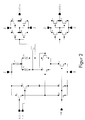
- the converter from ECL to CMOS consists of one input stage, one Level converter stage and an output stage together.
- the entrance stage consists of an emitter follower Q1, Q2, N3, N4.
- the level converter stage is an NFET differential stage N1, N2, N5, R1, R2, R3.
- the following Output stage consists of CMOS inverters P1 / N6, P2 / N7, P3 / N8, P4 / N9 together for pulse shaping.
- the dimensioning of this level converter is such that for a given Current through the level converter (determined by Vref) the level for the High state is determined by the voltage drop across R1 and the level for the low state due to the voltage drop at R1 and R2 or R3 is determined.
- the differential stage is designed so that the transistors at a defined ECL input signal at the input stage either are switched through or blocked.
- the differential stage either depends on the gate potentials N1 or N2 conductive. Is e.g. N1 (due to a higher gate potential than at N2) switched on, the current flows through R1, R2, N1 and N5.
- the Drain potential LS + of N1 then has low potential (voltage drop at R1 and R2) and the drain potential LS- of N2 then has high potential (only Voltage drop at R1 because no current flows through R3).
- the through R1 and R2 / R3 set levels should be symmetrical to the switching threshold of the controlled CMOS inverters P1 / N6, P3 / N8 be around a fast Switching to achieve.
- FIG. 3 explains how a converter from ECL to CMOS is used with additional regulation of the switching threshold a further reduction the switchover time without increasing the power loss.
- the switching time is reduced without the power loss increase.
- the reference voltage is applied the current source transistors N3, N4, N5 regulated.
- This rule standard is used by an operational amplifier OpAmp with a artificially generated voltage compared to the center of the signal swing of the Difference level corresponds.
- the scheme consists of the Operational amplifier OpAmp, a replica or dummy P1_D, N6_D of the CMOS inverter P3, N8 or P1, N6 and a replica R1_D, R2A_D, R2B_D, N5_D of the differential stage N1, N2, N5, R1, R2, R3.
- R1_D has the same value as R1 and N5_D has the same dimensions as N5.
- the resistance R2 of the Difference level was divided into two equally large resistors R2A_D and R2B_D divided up.
- the voltage between the resistors R2A_D and R2B_D the simulation R1_D, R2A_D, R2B_D, N5_D of the differential level N1, N2, N5, R1, R2, R3 corresponds exactly to the middle of the signal swing between LS + and LS-.
- the switching threshold of the CMOS inverters P1, N6 or P3, N8 is determined by a short circuit of the replica P1_D, N6_D of the CMOS inverter generated.
- the operational amplifier OpAmp pulls over the regulation of the Current through N5_D the artificial center potential in the simulation of the Difference level to the switching threshold of the CMOS inverter.
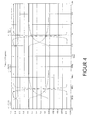
- FIG. 4 shows the level curves on the ECL / CMOS level converter for a Operating voltage of 2.5 volts.
- ECL + / ECL- are the differential ECL Input signals with a signal swing of 200mV
- LS + / LS- are the Output voltages of the level converter
- CMOS + / CMOS- shows the CMOS output signals.
Landscapes
- Engineering & Computer Science (AREA)
- Computer Hardware Design (AREA)
- Physics & Mathematics (AREA)
- Computing Systems (AREA)
- General Engineering & Computer Science (AREA)
- Mathematical Physics (AREA)
- Logic Circuits (AREA)
- Analogue/Digital Conversion (AREA)
- Semiconductor Integrated Circuits (AREA)
Abstract
Description
Claims (5)
- Konverter von ECL nach CMOS mit einer Eingangsstufe (Q1, Q2, N3, N4), einer Pegelwandlerstufe (N1, N2, N5, R1, R2, R3) und einer Ausgangsstufe (P1, P2, P3, P4, N6, N7, N8, N9), dadurch gekennzeichnet, dass die Pegelwandlerstufe (N1, N2, N5, R1, R2, R3) eine NFET Differenzstufe N1, N2 aufweist.
- Der Konverter von ECL nach CMOS nach Anspruch 1, dadurch gekennzeichnet, dass die Eingangsstufe (Q1, Q2, N3, N4) und/oder die Pegelwandlerstufe (N1, N2, N5, R1, R2, R3) eine Regelung der Umschaltschwelle hat.
- Der Konverter von ECL nach CMOS nach Anspruch 2, dadurch gekennzeichnet, dass der Konverter Mittel zur Generierung einer Referenzspannung für Stromquellentransistoren (N3, N4, N5) umfasst, zur Regelung der Umschaltschwelle.
- Der Konverter von ECL nach CMOS nach Anspruch 3, dadurch gekennzeichnet, dass die Mittel zur Generierung einer Referenzspannung eine Nachbildung (P1_D, N6_D, OpAmp, N5_D, R1_D, R2A_D. R2B_D) von Teilen des Konverters zur Ermittlung der Referenzspannung aufweisen.
- Ein Netzwerkelement zum Übertragen von Signalen, das einen Konverter von ECL nach CMOS mit einer Eingangsstufe (Q1, Q2, N3, N4), einer Pegelwandlerstufe (N1, N2, N5, R1, R2, R3) und einer Ausgangsstufe (P1, P2, P3, P4, N6, N7, N8, N9) umfasst, dadurch gekennzeichnet, dass die Pegelwandlerstufe (N1, N2, N5, R1, R2, R3) eine NFET Differenzstufe N1, N2 aufweist.
Priority Applications (4)
| Application Number | Priority Date | Filing Date | Title |
|---|---|---|---|
| DE50210601T DE50210601D1 (de) | 2002-12-18 | 2002-12-18 | Ein Konverter von ECL nach CMOS für ein digitales Netzwerk |
| AT02360362T ATE368960T1 (de) | 2002-12-18 | 2002-12-18 | Ein konverter von ecl nach cmos für ein digitales netzwerk |
| EP02360362A EP1432125B1 (de) | 2002-12-18 | 2002-12-18 | Ein Konverter von ECL nach CMOS für ein digitales Netzwerk |
| US10/716,475 US6956400B2 (en) | 2002-12-18 | 2003-11-20 | Converter from ECL to CMOS and network element for transmitting signals |
Applications Claiming Priority (1)
| Application Number | Priority Date | Filing Date | Title |
|---|---|---|---|
| EP02360362A EP1432125B1 (de) | 2002-12-18 | 2002-12-18 | Ein Konverter von ECL nach CMOS für ein digitales Netzwerk |
Publications (2)
| Publication Number | Publication Date |
|---|---|
| EP1432125A1 true EP1432125A1 (de) | 2004-06-23 |
| EP1432125B1 EP1432125B1 (de) | 2007-08-01 |
Family
ID=32338219
Family Applications (1)
| Application Number | Title | Priority Date | Filing Date |
|---|---|---|---|
| EP02360362A Expired - Lifetime EP1432125B1 (de) | 2002-12-18 | 2002-12-18 | Ein Konverter von ECL nach CMOS für ein digitales Netzwerk |
Country Status (4)
| Country | Link |
|---|---|
| US (1) | US6956400B2 (de) |
| EP (1) | EP1432125B1 (de) |
| AT (1) | ATE368960T1 (de) |
| DE (1) | DE50210601D1 (de) |
Families Citing this family (4)
| Publication number | Priority date | Publication date | Assignee | Title |
|---|---|---|---|---|
| JP2006054886A (ja) * | 2004-08-09 | 2006-02-23 | Samsung Electronics Co Ltd | ロー漏洩電流を持つレベルシフタ |
| KR100587689B1 (ko) * | 2004-08-09 | 2006-06-08 | 삼성전자주식회사 | 반도체 장치에 적합한 레벨 시프트 회로 |
| TWI234931B (en) * | 2004-08-10 | 2005-06-21 | Via Tech Inc | Level shifter |
| US7928765B2 (en) * | 2009-03-30 | 2011-04-19 | Lsi Corporation | Tuning high-side and low-side CMOS data-paths in CML-to-CMOS signal converter |
Citations (5)
| Publication number | Priority date | Publication date | Assignee | Title |
|---|---|---|---|---|
| BE1004501A3 (nl) * | 1989-06-28 | 1992-12-01 | Bell Telephone Mfg | Versterkerinrichting. |
| JPH06152379A (ja) * | 1992-10-30 | 1994-05-31 | Fujitsu Ltd | レベル変換回路 |
| JPH06232726A (ja) * | 1993-02-02 | 1994-08-19 | Hitachi Ltd | 入力回路、及び半導体集積回路 |
| JPH06268599A (ja) * | 1993-03-10 | 1994-09-22 | Hitachi Ltd | 装置間接続装置 |
| JP2002319857A (ja) * | 2001-04-20 | 2002-10-31 | Nec Eng Ltd | レベル変換回路 |
Family Cites Families (7)
| Publication number | Priority date | Publication date | Assignee | Title |
|---|---|---|---|---|
| US4471244A (en) * | 1981-07-22 | 1984-09-11 | Data General Corporation | Sense amplifier |
| JP3008422B2 (ja) * | 1990-02-01 | 2000-02-14 | 日本電気株式会社 | Ecl―cmosレベル変換回路 |
| US5264745A (en) * | 1992-08-28 | 1993-11-23 | Advanced Micro Devices, Inc. | Recovering phase and data from distorted duty cycles caused by ECL-to-CMOS translator |
| JP3538442B2 (ja) * | 1993-09-20 | 2004-06-14 | 富士通株式会社 | レベル変換回路 |
| US5426381A (en) * | 1994-05-23 | 1995-06-20 | Motorola Inc. | Latching ECL to CMOS input buffer circuit |
| US5724361A (en) * | 1996-03-12 | 1998-03-03 | Lsi Logic Corporation | High performance n:1 multiplexer with overlap control of multi-phase clocks |
| US6252421B1 (en) * | 1998-07-27 | 2001-06-26 | Texas Instruments Incorporated | Differential, high speed, ECL to CMOS converter |
-
2002
- 2002-12-18 EP EP02360362A patent/EP1432125B1/de not_active Expired - Lifetime
- 2002-12-18 DE DE50210601T patent/DE50210601D1/de not_active Expired - Lifetime
- 2002-12-18 AT AT02360362T patent/ATE368960T1/de not_active IP Right Cessation
-
2003
- 2003-11-20 US US10/716,475 patent/US6956400B2/en not_active Expired - Lifetime
Patent Citations (5)
| Publication number | Priority date | Publication date | Assignee | Title |
|---|---|---|---|---|
| BE1004501A3 (nl) * | 1989-06-28 | 1992-12-01 | Bell Telephone Mfg | Versterkerinrichting. |
| JPH06152379A (ja) * | 1992-10-30 | 1994-05-31 | Fujitsu Ltd | レベル変換回路 |
| JPH06232726A (ja) * | 1993-02-02 | 1994-08-19 | Hitachi Ltd | 入力回路、及び半導体集積回路 |
| JPH06268599A (ja) * | 1993-03-10 | 1994-09-22 | Hitachi Ltd | 装置間接続装置 |
| JP2002319857A (ja) * | 2001-04-20 | 2002-10-31 | Nec Eng Ltd | レベル変換回路 |
Non-Patent Citations (4)
| Title |
|---|
| PATENT ABSTRACTS OF JAPAN vol. 018, no. 467 (E - 1599) 30 August 1994 (1994-08-30) * |
| PATENT ABSTRACTS OF JAPAN vol. 018, no. 603 (E - 1632) 16 November 1994 (1994-11-16) * |
| PATENT ABSTRACTS OF JAPAN vol. 018, no. 675 (E - 1648) 20 December 1994 (1994-12-20) * |
| PATENT ABSTRACTS OF JAPAN vol. 2003, no. 02 5 February 2003 (2003-02-05) * |
Also Published As
| Publication number | Publication date |
|---|---|
| US20040119498A1 (en) | 2004-06-24 |
| US6956400B2 (en) | 2005-10-18 |
| DE50210601D1 (de) | 2007-09-13 |
| EP1432125B1 (de) | 2007-08-01 |
| ATE368960T1 (de) | 2007-08-15 |
Similar Documents
| Publication | Publication Date | Title |
|---|---|---|
| DE19919140B4 (de) | Niederspannungs-Differenzsignaltreiber mit Vorverstärkerschaltung | |
| DE69524265T2 (de) | Spannungspegelverschieber | |
| DE69839067T2 (de) | Regelwandlerschaltung und integrierte Halbleiterschaltung, in der diese verwendet wird | |
| DE69924173T2 (de) | Integrierte Halbleiterschaltung mit Schlafmodus mit geringem Stromverbrauch und geringem Flächenbedarf | |
| DE69117553T2 (de) | Ausgangsschaltung | |
| DE3627681C2 (de) | ||
| DE3685804T2 (de) | Ttl/cmos-kompatible eingangspufferschaltung. | |
| DE3906927C2 (de) | ||
| DE102004012239A1 (de) | Schaltung zum Transformieren eines Signals in einem Differenzmodus in ein unsymmetrisches Signal bei reduzierter Leistungsaufnahme im Standby-Zustand | |
| DE4344307C2 (de) | Ausgangsschaltung einer integrierten Halbleiterschaltkreisvorrichtung | |
| DE3342336A1 (de) | Schnittstellenschaltung | |
| DE10226066A1 (de) | Pegelverschiebungsumkehrschaltung und Leistungshalbleitervorrichtung | |
| DE69834755T2 (de) | Ausgangsschaltung, Eingangsschaltung und Eingangs/Ausgangsschaltung | |
| DE69118214T2 (de) | Digitaler Halbleiterschaltkreis | |
| DE69612007T2 (de) | Ausgangspuffer mit gemeinsam genutzten zwischenknoten | |
| DE19818021A1 (de) | Eingangspuffer mit einer Hysteresecharakteristik | |
| DE69519386T2 (de) | Digitale Spannungspegelumsetzer und Systeme damit | |
| DE69802631T2 (de) | Differentielle CMOS Logikfamilie | |
| DE4133902A1 (de) | Cmos-leistungsverstaerker | |
| DE19637444A1 (de) | Eingabeschaltungsvorrichtung | |
| WO2003043191A2 (de) | Lvds-treiber für kleine versorgungsspannungen | |
| DE69624016T2 (de) | CMOS-PECL-Pegelumsetzungsschaltung | |
| DE4107870C2 (de) | ||
| DE19937829A1 (de) | Schaltung, Verfahren und Vorrichtung zum Ausgeben, Eingeben bzw. Empfangen von Daten | |
| DE69735659T2 (de) | Differenzsignal-Generatorschaltung mit einer Schaltung zur Stromspitzenunterdrückung |
Legal Events
| Date | Code | Title | Description |
|---|---|---|---|
| PUAI | Public reference made under article 153(3) epc to a published international application that has entered the european phase |
Free format text: ORIGINAL CODE: 0009012 |
|
| 17P | Request for examination filed |
Effective date: 20030709 |
|
| AK | Designated contracting states |
Kind code of ref document: A1 Designated state(s): AT BE BG CH CY CZ DE DK EE ES FI FR GB GR IE IT LI LU MC NL PT SE SI SK TR |
|
| AX | Request for extension of the european patent |
Extension state: AL LT LV MK RO |
|
| AKX | Designation fees paid |
Designated state(s): AT BE BG CH CY CZ DE DK EE ES FI FR GB GR IE IT LI LU MC NL PT SE SI SK TR |
|
| GRAP | Despatch of communication of intention to grant a patent |
Free format text: ORIGINAL CODE: EPIDOSNIGR1 |
|
| RAP1 | Party data changed (applicant data changed or rights of an application transferred) |
Owner name: ALCATEL LUCENT |
|
| GRAS | Grant fee paid |
Free format text: ORIGINAL CODE: EPIDOSNIGR3 |
|
| GRAA | (expected) grant |
Free format text: ORIGINAL CODE: 0009210 |
|
| AK | Designated contracting states |
Kind code of ref document: B1 Designated state(s): AT BE BG CH CY CZ DE DK EE ES FI FR GB GR IE IT LI LU MC NL PT SE SI SK TR |
|
| REG | Reference to a national code |
Ref country code: GB Ref legal event code: FG4D Free format text: NOT ENGLISH |
|
| REG | Reference to a national code |
Ref country code: CH Ref legal event code: EP |
|
| REG | Reference to a national code |
Ref country code: IE Ref legal event code: FG4D Free format text: LANGUAGE OF EP DOCUMENT: GERMAN |
|
| REF | Corresponds to: |
Ref document number: 50210601 Country of ref document: DE Date of ref document: 20070913 Kind code of ref document: P |
|
| GBT | Gb: translation of ep patent filed (gb section 77(6)(a)/1977) |
Effective date: 20070830 |
|
| ET | Fr: translation filed | ||
| PG25 | Lapsed in a contracting state [announced via postgrant information from national office to epo] |
Ref country code: BG Free format text: LAPSE BECAUSE OF FAILURE TO SUBMIT A TRANSLATION OF THE DESCRIPTION OR TO PAY THE FEE WITHIN THE PRESCRIBED TIME-LIMIT Effective date: 20071101 Ref country code: NL Free format text: LAPSE BECAUSE OF FAILURE TO SUBMIT A TRANSLATION OF THE DESCRIPTION OR TO PAY THE FEE WITHIN THE PRESCRIBED TIME-LIMIT Effective date: 20070801 Ref country code: ES Free format text: LAPSE BECAUSE OF FAILURE TO SUBMIT A TRANSLATION OF THE DESCRIPTION OR TO PAY THE FEE WITHIN THE PRESCRIBED TIME-LIMIT Effective date: 20071112 Ref country code: FI Free format text: LAPSE BECAUSE OF FAILURE TO SUBMIT A TRANSLATION OF THE DESCRIPTION OR TO PAY THE FEE WITHIN THE PRESCRIBED TIME-LIMIT Effective date: 20070801 |
|
| NLV1 | Nl: lapsed or annulled due to failure to fulfill the requirements of art. 29p and 29m of the patents act | ||
| REG | Reference to a national code |
Ref country code: IE Ref legal event code: FD4D |
|
| PG25 | Lapsed in a contracting state [announced via postgrant information from national office to epo] |
Ref country code: DK Free format text: LAPSE BECAUSE OF FAILURE TO SUBMIT A TRANSLATION OF THE DESCRIPTION OR TO PAY THE FEE WITHIN THE PRESCRIBED TIME-LIMIT Effective date: 20070801 Ref country code: GR Free format text: LAPSE BECAUSE OF FAILURE TO SUBMIT A TRANSLATION OF THE DESCRIPTION OR TO PAY THE FEE WITHIN THE PRESCRIBED TIME-LIMIT Effective date: 20071102 |
|
| PG25 | Lapsed in a contracting state [announced via postgrant information from national office to epo] |
Ref country code: SK Free format text: LAPSE BECAUSE OF FAILURE TO SUBMIT A TRANSLATION OF THE DESCRIPTION OR TO PAY THE FEE WITHIN THE PRESCRIBED TIME-LIMIT Effective date: 20070801 Ref country code: PT Free format text: LAPSE BECAUSE OF FAILURE TO SUBMIT A TRANSLATION OF THE DESCRIPTION OR TO PAY THE FEE WITHIN THE PRESCRIBED TIME-LIMIT Effective date: 20080102 Ref country code: IE Free format text: LAPSE BECAUSE OF FAILURE TO SUBMIT A TRANSLATION OF THE DESCRIPTION OR TO PAY THE FEE WITHIN THE PRESCRIBED TIME-LIMIT Effective date: 20070801 Ref country code: CZ Free format text: LAPSE BECAUSE OF FAILURE TO SUBMIT A TRANSLATION OF THE DESCRIPTION OR TO PAY THE FEE WITHIN THE PRESCRIBED TIME-LIMIT Effective date: 20070801 |
|
| PLBE | No opposition filed within time limit |
Free format text: ORIGINAL CODE: 0009261 |
|
| STAA | Information on the status of an ep patent application or granted ep patent |
Free format text: STATUS: NO OPPOSITION FILED WITHIN TIME LIMIT |
|
| BERE | Be: lapsed |
Owner name: ALCATEL LUCENT Effective date: 20071231 |
|
| PG25 | Lapsed in a contracting state [announced via postgrant information from national office to epo] |
Ref country code: SE Free format text: LAPSE BECAUSE OF FAILURE TO SUBMIT A TRANSLATION OF THE DESCRIPTION OR TO PAY THE FEE WITHIN THE PRESCRIBED TIME-LIMIT Effective date: 20071101 |
|
| 26N | No opposition filed |
Effective date: 20080506 |
|
| PG25 | Lapsed in a contracting state [announced via postgrant information from national office to epo] |
Ref country code: MC Free format text: LAPSE BECAUSE OF NON-PAYMENT OF DUE FEES Effective date: 20071231 |
|
| REG | Reference to a national code |
Ref country code: CH Ref legal event code: PL |
|
| PG25 | Lapsed in a contracting state [announced via postgrant information from national office to epo] |
Ref country code: BE Free format text: LAPSE BECAUSE OF NON-PAYMENT OF DUE FEES Effective date: 20071231 |
|
| PG25 | Lapsed in a contracting state [announced via postgrant information from national office to epo] |
Ref country code: CH Free format text: LAPSE BECAUSE OF NON-PAYMENT OF DUE FEES Effective date: 20071231 Ref country code: LI Free format text: LAPSE BECAUSE OF NON-PAYMENT OF DUE FEES Effective date: 20071231 |
|
| PG25 | Lapsed in a contracting state [announced via postgrant information from national office to epo] |
Ref country code: EE Free format text: LAPSE BECAUSE OF FAILURE TO SUBMIT A TRANSLATION OF THE DESCRIPTION OR TO PAY THE FEE WITHIN THE PRESCRIBED TIME-LIMIT Effective date: 20070801 |
|
| PG25 | Lapsed in a contracting state [announced via postgrant information from national office to epo] |
Ref country code: AT Free format text: LAPSE BECAUSE OF NON-PAYMENT OF DUE FEES Effective date: 20071218 |
|
| PG25 | Lapsed in a contracting state [announced via postgrant information from national office to epo] |
Ref country code: SI Free format text: LAPSE BECAUSE OF FAILURE TO SUBMIT A TRANSLATION OF THE DESCRIPTION OR TO PAY THE FEE WITHIN THE PRESCRIBED TIME-LIMIT Effective date: 20070801 |
|
| PG25 | Lapsed in a contracting state [announced via postgrant information from national office to epo] |
Ref country code: CY Free format text: LAPSE BECAUSE OF FAILURE TO SUBMIT A TRANSLATION OF THE DESCRIPTION OR TO PAY THE FEE WITHIN THE PRESCRIBED TIME-LIMIT Effective date: 20070801 |
|
| PG25 | Lapsed in a contracting state [announced via postgrant information from national office to epo] |
Ref country code: LU Free format text: LAPSE BECAUSE OF NON-PAYMENT OF DUE FEES Effective date: 20071218 |
|
| PG25 | Lapsed in a contracting state [announced via postgrant information from national office to epo] |
Ref country code: TR Free format text: LAPSE BECAUSE OF FAILURE TO SUBMIT A TRANSLATION OF THE DESCRIPTION OR TO PAY THE FEE WITHIN THE PRESCRIBED TIME-LIMIT Effective date: 20070801 |
|
| PG25 | Lapsed in a contracting state [announced via postgrant information from national office to epo] |
Ref country code: IT Free format text: LAPSE BECAUSE OF NON-PAYMENT OF DUE FEES Effective date: 20071231 |
|
| REG | Reference to a national code |
Ref country code: GB Ref legal event code: 732E Free format text: REGISTERED BETWEEN 20130926 AND 20131002 |
|
| REG | Reference to a national code |
Ref country code: FR Ref legal event code: GC Effective date: 20131018 |
|
| REG | Reference to a national code |
Ref country code: FR Ref legal event code: CA Effective date: 20150521 |
|
| REG | Reference to a national code |
Ref country code: FR Ref legal event code: CA Effective date: 20150521 |
|
| REG | Reference to a national code |
Ref country code: FR Ref legal event code: PLFP Year of fee payment: 14 |
|
| REG | Reference to a national code |
Ref country code: FR Ref legal event code: PLFP Year of fee payment: 15 |
|
| PGFP | Annual fee paid to national office [announced via postgrant information from national office to epo] |
Ref country code: DE Payment date: 20161213 Year of fee payment: 15 Ref country code: GB Payment date: 20161222 Year of fee payment: 15 |
|
| PGFP | Annual fee paid to national office [announced via postgrant information from national office to epo] |
Ref country code: FR Payment date: 20161222 Year of fee payment: 15 |
|
| REG | Reference to a national code |
Ref country code: DE Ref legal event code: R119 Ref document number: 50210601 Country of ref document: DE |
|
| GBPC | Gb: european patent ceased through non-payment of renewal fee |
Effective date: 20171218 |
|
| REG | Reference to a national code |
Ref country code: FR Ref legal event code: ST Effective date: 20180831 |
|
| PG25 | Lapsed in a contracting state [announced via postgrant information from national office to epo] |
Ref country code: DE Free format text: LAPSE BECAUSE OF NON-PAYMENT OF DUE FEES Effective date: 20180703 Ref country code: FR Free format text: LAPSE BECAUSE OF NON-PAYMENT OF DUE FEES Effective date: 20180102 |
|
| PG25 | Lapsed in a contracting state [announced via postgrant information from national office to epo] |
Ref country code: GB Free format text: LAPSE BECAUSE OF NON-PAYMENT OF DUE FEES Effective date: 20171218 |