EP1429283A2 - Tragbarer Datenträger - Google Patents
Tragbarer Datenträger Download PDFInfo
- Publication number
- EP1429283A2 EP1429283A2 EP03028151A EP03028151A EP1429283A2 EP 1429283 A2 EP1429283 A2 EP 1429283A2 EP 03028151 A EP03028151 A EP 03028151A EP 03028151 A EP03028151 A EP 03028151A EP 1429283 A2 EP1429283 A2 EP 1429283A2
- Authority
- EP
- European Patent Office
- Prior art keywords
- chip card
- interface
- contact tongue
- contact
- chip
- Prior art date
- Legal status (The legal status is an assumption and is not a legal conclusion. Google has not performed a legal analysis and makes no representation as to the accuracy of the status listed.)
- Granted
Links
Images


Classifications
-
- G—PHYSICS
- G06—COMPUTING OR CALCULATING; COUNTING
- G06K—GRAPHICAL DATA READING; PRESENTATION OF DATA; RECORD CARRIERS; HANDLING RECORD CARRIERS
- G06K19/00—Record carriers for use with machines and with at least a part designed to carry digital markings
- G06K19/06—Record carriers for use with machines and with at least a part designed to carry digital markings characterised by the kind of the digital marking, e.g. shape, nature, code
- G06K19/067—Record carriers with conductive marks, printed circuits or semiconductor circuit elements, e.g. credit or identity cards also with resonating or responding marks without active components
- G06K19/07—Record carriers with conductive marks, printed circuits or semiconductor circuit elements, e.g. credit or identity cards also with resonating or responding marks without active components with integrated circuit chips
- G06K19/077—Constructional details, e.g. mounting of circuits in the carrier
- G06K19/0772—Physical layout of the record carrier
- G06K19/07732—Physical layout of the record carrier the record carrier having a housing or construction similar to well-known portable memory devices, such as SD cards, USB or memory sticks
-
- G—PHYSICS
- G06—COMPUTING OR CALCULATING; COUNTING
- G06K—GRAPHICAL DATA READING; PRESENTATION OF DATA; RECORD CARRIERS; HANDLING RECORD CARRIERS
- G06K19/00—Record carriers for use with machines and with at least a part designed to carry digital markings
- G06K19/04—Record carriers for use with machines and with at least a part designed to carry digital markings characterised by the shape
- G06K19/041—Constructional details
-
- G—PHYSICS
- G06—COMPUTING OR CALCULATING; COUNTING
- G06K—GRAPHICAL DATA READING; PRESENTATION OF DATA; RECORD CARRIERS; HANDLING RECORD CARRIERS
- G06K19/00—Record carriers for use with machines and with at least a part designed to carry digital markings
- G06K19/06—Record carriers for use with machines and with at least a part designed to carry digital markings characterised by the kind of the digital marking, e.g. shape, nature, code
- G06K19/067—Record carriers with conductive marks, printed circuits or semiconductor circuit elements, e.g. credit or identity cards also with resonating or responding marks without active components
- G06K19/07—Record carriers with conductive marks, printed circuits or semiconductor circuit elements, e.g. credit or identity cards also with resonating or responding marks without active components with integrated circuit chips
- G06K19/077—Constructional details, e.g. mounting of circuits in the carrier
- G06K19/0772—Physical layout of the record carrier
- G06K19/07733—Physical layout of the record carrier the record carrier containing at least one further contact interface not conform ISO-7816
-
- G—PHYSICS
- G06—COMPUTING OR CALCULATING; COUNTING
- G06K—GRAPHICAL DATA READING; PRESENTATION OF DATA; RECORD CARRIERS; HANDLING RECORD CARRIERS
- G06K19/00—Record carriers for use with machines and with at least a part designed to carry digital markings
- G06K19/06—Record carriers for use with machines and with at least a part designed to carry digital markings characterised by the kind of the digital marking, e.g. shape, nature, code
- G06K19/067—Record carriers with conductive marks, printed circuits or semiconductor circuit elements, e.g. credit or identity cards also with resonating or responding marks without active components
- G06K19/07—Record carriers with conductive marks, printed circuits or semiconductor circuit elements, e.g. credit or identity cards also with resonating or responding marks without active components with integrated circuit chips
- G06K19/077—Constructional details, e.g. mounting of circuits in the carrier
- G06K19/07743—External electrical contacts
Definitions
- Chip cards which are also referred to as smart cards or memory cards , are known in a variety of configurations.
- chip cards have a thin card body in which there is at least one semiconductor chip.
- chip cards usually meet the requirements of the ISO 7810 standard.
- the contact-based chip cards in particular considered here are also generally designed in accordance with the ISO / IEC 7816 standard. Part 1 of this standard defines the physical properties of the chip card; Part 2 specifies the arrangement and design of the contact arrangement on the chip card, and part 3 defines electrical properties and transmission protocols.
- the standards mentioned are available from the International Organization for Standardization, Geneva, http: llwww.iso.ch .
- Chip cards are known from the international patent publications WO 00/16255 A1 and WO 01/69881 A2 which have two interfaces, namely a first interface according to the ISO / IEC 7816 standard and a second interface according to the USB standard.
- USB universal Serial Bus Specification
- the term “USB” is understood to mean the universal serial bus as available in the document “ Universal Serial Bus Specification ” of the USB Implementors Forum, Inc., Revision 2.0, April 27, 2000 http: // www.usb.orgldevelopersldocs.html .
- a portable data carrier in the form of a chip card with at least one Interface that uses interface contacts, which on a contact tongue the chip card are arranged.
- the invention is based on the basic idea, at least interface contacts an interface on a formed from the portable data carrier Provide contact tongue.
- the portable data carrier is a chip card
- This external socket is a flat socket, which the Contact tongue encloses at least on the side.
- the socket a USB socket of type "A”.
- the width of one for insertion into one such socket designed contact tongue is approximately 12 mm. This is narrower than the widths of the three common ones, through the ISO 7810 standard defined chip card formats ID-1, ID-00 and ID-000.
- the first and the second interface preferably use at least partially different interface contacts.
- at least one additional interface contact may be provided, an interface contact that is not used for the first interface becomes.
- This at least one additional interface contact the second
- the interface is in the contact arrangement of the integrated first interface or is in the immediate vicinity this contact arrangement.
- the Contact arrangement of the first interface and the additional one / s In contrast, interface contact (s) spatially on the surface of the chip card separated from each other.
- the contact tongue is in an inner area the chip card is formed, which is separated on all sides from the outer edge of the chip card is.
- the contact tongue can be formed in that the Chip card is provided with a U-shaped slot. The one from this slot Surrounded inner area of the chip card forms the contact tongue.
- the contact tongue can also be configured at the edge of the chip card be arranged. This also includes embodiments in which the Contact tongue begins in an inner area of the chip card and on the edge of the card format defined by the ISO 7810 standard ends.
- the contact tongue faces laterally attached, foldable webs to e.g. a USB plug with a greater thickness than the chip card thickness.
- the contact tongue forms preferably a permanent part of the chip card, so that a repeated and alternating use of the first and the second Interface is possible. This represents another distinguishing feature of the present chip card to the chip cards known in the field of mobile phones which, on a carrier card in the ID-1 format, is an irreversibly breakable Compact chip card in ID-000 format included.
- Embodiments of the chip card, in which the second interface is a USB interface are particularly suitable for connecting the chip card currently common computers. All active are preferred Interface contacts of the chip card with at least one semiconductor chip connected, which - for example to those in the documents WO 00/16255 A1 and WO 01/69881 A2 described way - the electrical Receives, sends and processes signals from both interfaces.
- a preferred field of application of the invention is so-called internet chip cards, who implement a compact internet server.
- One on an external computer running Internet browser communicates via the second interface - e.g. the USB interface - with the server and provides one User interface ready for interaction with the chip card.
- the invention is but also useful for many other areas of application, e.g. always then, if there is extensive data between a chip card and an external device should be transferred.
- the External dimensions of the portable data carrier and the location of the interface then chosen so that the data carrier on the interface side is fully closed a compatible USB connector.
- this one Execution also the thickness of the card body to the conditions in a USB socket customized.
- Portable data carriers designed in this way are suitable in particular as software keys or "tokens" executed in hardware e.g. the authorization of a user to use a device is proven. Such tokens can be advantageously used by means of common ones Manufacture manufacturing methods as used in chip card production become.
- Fig. 1 shows a portable data carrier 1 in the form of a chip card with a Card body 2, in which a module 3 is embedded, in which there is a semiconductor chip with an integrated circuit 4, and a contact arrangement 10.
- the external dimensions of the chip card correspond to the ID-1 format the ISO 7810 standard.
- the chip card has a first and a second interface for communication with external devices.
- the first interface a "common" smart card interface, in its physical and electrical Properties and the protocols used in the standard Corresponds to ISO / IEC 7816.
- the second interface is here Embodiment a USB interface, by means of which the chip card directly to a computer or other with a USB "A" socket equipped device can be connected.
- the Chip card a contact arrangement 10, which is shown in more detail in Fig. 4.
- the contact arrangement 10 also includes part 2 of the standard ISO / IEC 7816 defined positions a total of eight interface contacts C 1, C2, C3, C4, C5, C6, C7, C8 of the first interface. Furthermore are in the contact arrangement 10 according to FIG. 1 and FIG. 4 a total of four further interface contacts CA, CB, CC, CD integrated, assigned to the second interface are.
- all interface contacts are C1 - C8 and CA - CD as approximately flush with the chip card surface Designed contact surfaces, while in modifications, in particular for the additional interface contacts CA - CD other designs can be provided.
- the contact arrangement 10 is located on a contact tongue 12, which in the present Embodiment is formed in that a three-sided circumferential, U-shaped slot worked into the carrier material of the chip card is.
- the contact tongue 12 integrally merges into the rest of the chip card.
- the fat 13 of the contact tongue 12 corresponds to the standard thickness of the chip card.
- the Contact arrangement 10 On the tip of the contact tongue shown in Fig. 1 is the Contact arrangement 10.
- the width of the contact tongue 12 is here Embodiment approximately 12 mm, while the contact arrangement 10 - according to part 2 of the ISO / IEC 7816 standard - from the upper edge of the contact field CA a minimum size of approximately to the lower edge of the contact field CD 9.3 mm.
- a is used as the material for the card body flexible plastic material, such as PVC, ABS or PET, used.
- the carrier material of the chip card is in a manner known per se Semiconductor chip incorporated, which is covered by the contact field 10 in FIG. 1.
- the card body can also be of particularly high quality in alternative designs Materials such as film composites or metals have a high Ensure lifespan. This is especially true for those below Design variants according to FIGS. 6-10 to be described in more detail.
- the smart card can be in its flat configuration, shown in FIG used as a standard ISO / IEC-7816 chip card and for example in one Card terminal or a card reader are introduced.
- the one in the chip card located semiconductor chip recognizes this first mode of operation and provides electrical and logically an ISO / IEC-7816-compatible interface is available, whose Signals via the eight interface contacts C1 - C8 of the contact arrangement 10 be performed.
- the chip card can be inserted directly into the USB socket 16 inserted, for example, of a computer or other device become.
- the semiconductor chip of the chip card also adapts to this second operating mode by using an electrically and logically USB compatible interface provides whose signals via the four additional interface contacts CA - CD run. If the chip card is pulled out of the USB socket 16, so the contact tongue 12 bends due to the elasticity of the chip card backing used in the chip card level, so that again flat configuration according to FIG. 1 is reached.
- FIG. 5 shows an arrangement of the interface contacts modified compared to FIG. 4 C1 - C8 and CA - CD.
- the additional interface contacts CA - CD of the second interface - here the USB interface - are here not integrated in the ISO / IEC-7816-compatible contact arrangement 10.
- Much more the additional interface contacts CA - CD are located immediately in addition to a contact arrangement 10 'which corresponds exactly to the standard ISO / IEC 7816 and only the eight provided in accordance with this standard Interface contacts C1 - C8 has. 5 enables the interface contacts CA - CD to be particularly close to the tip to arrange the contact tongue 12. Furthermore, it is avoided that the Contact springs 20A - 20D when the contact tongue 12 is inserted into the Briefly slide USB socket 16 over the interface contacts C1 - C4.
- the webs 22A, 22B can also be flattened again after use Configuration can be folded back, taking from accordingly widened areas of the slot 14 are added.
- FIG. 6 A illustrates an embodiment variant in which the height compensation from the thickness 13 of the contact tongue 12 to the height 17 of a USB socket 16 is achieved with the help of an additional filler card F.
- the filler card F corresponds to their dimensions of a chip card and has the same position as that Chip card a flexible tongue 12A. Its thickness is such that the Superimposing filler card and chip card resulting total thickness corresponds exactly to the height of a USB socket 16.
- At the top of the filler card F are connecting means designed to detachably the filling card on a chip card to be able to attach.
- the connection is made so that filler card and Chip card, so that contact tongue 12 and tongue 12 A, exactly one above the other lie.
- a connection means comes, for example, a reusable one Pressure sensitive adhesive layer into consideration.
- the connecting means can Include shaping that supports the connection. For example small bulges can be created on the filling card, which in corresponding recesses on the chip card grab.
- the filler card F which is generally handled separately, is used Chip card attached. Then the ones lying on top of each other Tongues 12, 12A bent out of the plane of the card and plugged together into the USB socket 16. Because of each other the pair of tongues 12, 12A sits firmly in the USB socket.
- the contact tongue 12 was in an inner area of the chip card, i.e. with an all-round distance from the outer Edge of the chip card, arranged.
- Fig. 8 Fig. 9 and Fig. 10 are against Embodiments shown in which the contact tongue 12 on the edge of Chip card is arranged.
- the contacts C1 - C8 of the first interface in the Contact arrangement 10 are spatially separated from the contacts CA - CD second interface removed. This has the advantage that in terms of Design of the interface contacts C1 - C8 and CA - CD less interdependencies and restrictions exist.
- the interface contacts CA - CD in FIGS. 8 to 10 with regard to their geometry largely or completely designed according to the USB standard his.
- the incisions 28A, 28B can also be wider in further embodiments be designed, in the extreme case so wide that the map areas above and drop completely below the contact tongue 12.
- Such a configuration is shown in Fig. 9.
- the chip card shown there can be used in almost any - also plug into a USB socket 16 that is permanently installed in a computer.
- the chip card does not correspond to its external dimensions more of the ISO 7810 standard, what when used in card readers or Card terminals could potentially cause difficulties. To such Problems are to be avoided in the embodiment according to FIG. 10 by the Standard ISO 7810 specified external dimensions as far as possible.
- the configurations described above are all based on the approach that the portable data carrier 1 has at least the functionality of a chip card has and accordingly two interfaces, namely an ISO and a USB interface having.
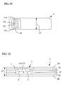
- FIGS. 11 and 12th illustrated embodiment of the proposed concept is reduced the portable data carrier 1 on a contact tongue 12 and has only one USB interface. In this way it functions e.g. as a security token for verification an authorization by means of one stored on the token Software key.
- the external dimensions of the portable shown in FIGS. 11, 12 Data carrier 1 no longer meet the ISO 7810 chip card standard, but instead are matched to a USB socket 16.
- the Card body 2 one on the level 17 of under the contact springs 20A - 20D a USB socket 16 lying space adapted, not standard Thickness 17 '.
- the increased thickness can be easily produced realize by the card body 2 in the usual way like a chip card several layers 2A - 2E, but a correspondingly thicker one Inner layer or additional inner layers 2B - 2D in the Card body structure are introduced.
- the contact arrangement 10 has, as in 11 illustrates exactly four interface contacts CA - CD, the Position on the position of the contact springs 20A - 20D of a USB socket 16 is aligned so that after inserting the data carrier 1 into a USB socket come to lie exactly under these.
- the contact arrangement 10 is expediently located, as in FIG. 12 indicated on the top of a module 3, on the underside of the integrated circuit 4 is arranged.
- the module 3 is preferably after Type of chip card module, i.e. based on a substrate 7, the one can be a suitable film, produced and embedded in the card body 2, typically into a recess 8 prepared therein. Only the shape the contact arrangement 10 is modified as a USB interface.
- integrated circuits 4 is in the Module 3 also expediently an additional integrated circuit 5 arranged, the function of which is to the integrated circuit 4th
- To provide auxiliary functions, in particular a clock signal, which for Operation of a chip card circuit on a USB interface required are.
Landscapes
- Engineering & Computer Science (AREA)
- Physics & Mathematics (AREA)
- General Physics & Mathematics (AREA)
- Theoretical Computer Science (AREA)
- Computer Hardware Design (AREA)
- Microelectronics & Electronic Packaging (AREA)
- Credit Cards Or The Like (AREA)
- Coupling Device And Connection With Printed Circuit (AREA)
- Reduction Or Emphasis Of Bandwidth Of Signals (AREA)
Abstract
Description
Claims (22)
- Tragbarer Datenträger mit einem Kartenkörper, in den ein integrierter Schaltkreis eingebettet ist, sowie mindestens einer Schnittstelle, dadurch gekennzeichnet, daß die Schnittstelle Schnittstellenkontakte (CA - CD) nutzt, die auf einer aus dem Kartenkörper (2) herausgeformten Kontaktzunge (12) angeordnet sind.
- Tragbarer Datenträger nach Anspruch 1, dadurch gekennzeichnet, daß die Schnittstelle eine USB-Schnittstelle ist.
- Tragbarer Datenträger nach Anspruch 2, dadurch gekennzeichnet, daß der Kartenkörper (2) aus mehreren Schichten (2A-2E) aufgebaut ist, wobei Höhe (17') und Breite (21') des Schichtaufbaus im Bereich der Kontaktzunge (12) paßgenau auf die Abmessungen des unter den Gegenkontakten (20A - 20D) befindlichen Steckraumes einer USB-Buchse (16) abgestimmt sind.
- Tragbarer Datenträger nach Anspruch 1, dadurch gekennzeichnet, daß der integrierte Schaltkreis (4) an der Unterseite eines in den Kartenkörper (2) eingesetzten Modules (3) angeordnet ist, an dessen Oberseite die Schnittstellenkontakte (CA ― CD) ausgebildet sind.
- Tragbarer Datenträger nach Anspruch 1, dadurch gekennzeichnet, daß in dem Modul (3) ein zweiter integrierter Schaltkreis (5) ausgebildet ist, der mit dem ersten verbunden ist und diesem ein Taktsignal liefert.
- Chipkarte nach Anspruch 1 gekennzeichnet dadurch, daß sie eine erste sowie eine zweite Schnittstelle aufweist, wobei die zweite Schnittstellenkontakte (CA - CD) nutzt, die auf einer Kontaktzunge (12) der Chipkarte angeordnet sind.
- Chipkarte nach Anspruch 6, dadurch gekennzeichnet, daß die erste und die zweite Schnittstelle zumindest teilweise unterschiedliche Schnittstellenkontakte (C1 - C8; CA - CD) nutzen.
- Chipkarte nach Anspruch 6 oder Anspruch 7, dadurch gekennzeichnet, daß die Schnittstellenkontakte (C1 - C8) der ersten Schnittstelle eine Kontaktanordnung (10') gemäß ISO/IEC 7816 oder eine damit kompatible Kontaktanordnung (10) bilden, und daß die zweite Schnittstelle zumindest teilweise zusätzliche Schnittstellenkontakte (CA - CD) nutzt.
- Chipkarte nach Anspruch 8, dadurch gekennzeichnet, daß die zusätzlichen Schnittstellenkontakte (CA - CD) der zweiten Schnittstelle in die Kontaktanordnung (10) der ersten Schnittstelle integriert oder der Kontaktanordnung (10') der ersten Schnittstelle benachbart angeordnet sind.
- Chipkarte nach einem der Ansprüche 6 bis 9, dadurch gekennzeichnet, daß die erste Schnittstelle eine Schnittstelle gemäß ISO/IEC 7816 ist.
- Chipkarte nach einem der Ansprüche 6 bis 10, dadurch gekennzeichnet, daß die zweite Schnittstelle eine USB-Schnittstelle ist.
- Chipkarte nach einem der Ansprüche 6 bis 11, dadurch gekennzeichnet, daß die Kontaktzunge (12) eine geringere Breite als die Chipkarte aufweist.
- Chipkarte nach einem der Ansprüche 6 bis 12, dadurch gekennzeichnet, daß die Kontaktzunge (12) einen dauerhaften Bestandteil der Chipkarte bildet.
- Chipkarte nach einem der Ansprüche 6 bis 13, dadurch gekennzeichnet, daß die Kontaktzunge (12) einstückig mit der restlichen Chipkarte ausgebildet ist.
- Chipkarte nach einem der Ansprüche 6 bis 14, dadurch gekennzeichnet, daß die Kontaktzunge (12) zum Einstecken in eine Flachbuchse, vorzugsweise eine USB-"A"-Buchse (16), eingerichtet ist.
- Chipkarte nach einem der Ansprüche 6 bis 15, dadurch gekennzeichnet, daß die Kontaktzunge (12) von der restlichen Chipkarte umgeben und von dieser durch einen U-förmigen Schlitz (14) getrennt ist.
- Chipkarte nach einem der Ansprüche 6 bis 16, dadurch gekennzeichnet, daß die Kontaktzunge (12) am Rand der Chipkarte angeordnet ist.
- Chipkarte nach einem der Ansprüche 6 bis 17, dadurch gekennzeichnet, daß die Kontaktzunge (12) aus der Chipkartenebene herausbiegbar oder herausklappbar und wieder in die Chipkartenebene zurückbiegbar oder zurückklappbar ist.
- Chipkarte nach Anspruch 18, dadurch gekennzeichnet, daß die Kontaktzunge (12) ein Scharnier (24) und/oder mindestens eine Schnapphalterung (26A - 26C) aufweist.
- Chipkarte nach einem der Ansprüche 6 bis 19, dadurch gekennzeichnet, daß die Kontaktzunge (12) in Höhe der auf ihr befindlichen Schnittstellenkontakte (CA - CD) der zweiten Schnittstelle mindestens einen seitlich angeordneten, klappbaren Steg (22A, 22B) aufweist.
- Füllkarte zur Verwendung zusammen mit einer Karte nach einem der Ansprüche 6 bis 20, dadurch gekennzeichnet, daß sie eine der Kontaktzunge (12) der Chipkarte entsprechende Zunge (12A) aufweist, die zusammen mit der Kontaktzunge (12) der Chipkarte aus der Chipkartenebene herausbiegbar oder herausklappbar und wieder in die Chipkartenebene zurückbiegbar oder zurückklappbar ist.
- Chipkarte nach einem der Ansprüche 6 bis 20, dadurch gekennzeichnet, daß die Chipkarte mindestens einen Halbleiterchip (4) aufweist, der zum Austausch von Daten sowohl über die erste als auch über die zweite Schnittstelle eingerichtet ist.
Priority Applications (1)
| Application Number | Priority Date | Filing Date | Title |
|---|---|---|---|
| EP06008084A EP1724713A3 (de) | 2002-12-12 | 2003-12-08 | Tragbarer Datenträger |
Applications Claiming Priority (4)
| Application Number | Priority Date | Filing Date | Title |
|---|---|---|---|
| DE10258158 | 2002-12-12 | ||
| DE10258158 | 2002-12-12 | ||
| DE10344049 | 2003-09-23 | ||
| DE10344049A DE10344049A1 (de) | 2002-12-12 | 2003-09-23 | Tragbarer Datenträger |
Related Child Applications (1)
| Application Number | Title | Priority Date | Filing Date |
|---|---|---|---|
| EP06008084A Division EP1724713A3 (de) | 2002-12-12 | 2003-12-08 | Tragbarer Datenträger |
Publications (3)
| Publication Number | Publication Date |
|---|---|
| EP1429283A2 true EP1429283A2 (de) | 2004-06-16 |
| EP1429283A3 EP1429283A3 (de) | 2004-07-14 |
| EP1429283B1 EP1429283B1 (de) | 2007-11-07 |
Family
ID=32327516
Family Applications (2)
| Application Number | Title | Priority Date | Filing Date |
|---|---|---|---|
| EP06008084A Withdrawn EP1724713A3 (de) | 2002-12-12 | 2003-12-08 | Tragbarer Datenträger |
| EP03028151A Expired - Lifetime EP1429283B1 (de) | 2002-12-12 | 2003-12-08 | Tragbarer Datenträger |
Family Applications Before (1)
| Application Number | Title | Priority Date | Filing Date |
|---|---|---|---|
| EP06008084A Withdrawn EP1724713A3 (de) | 2002-12-12 | 2003-12-08 | Tragbarer Datenträger |
Country Status (4)
| Country | Link |
|---|---|
| EP (2) | EP1724713A3 (de) |
| AT (1) | ATE377808T1 (de) |
| DE (2) | DE10344049A1 (de) |
| ES (1) | ES2294237T3 (de) |
Cited By (22)
| Publication number | Priority date | Publication date | Assignee | Title |
|---|---|---|---|---|
| WO2005031639A1 (de) * | 2003-09-23 | 2005-04-07 | Giesecke & Devrient Gmbh | Tragbarer datenträger |
| WO2005086086A1 (en) * | 2004-02-27 | 2005-09-15 | Imation Corp. | Credit card sized memory card with host connector |
| WO2006018230A1 (de) | 2004-08-12 | 2006-02-23 | Giesecke & Devrient Gmbh | Verfahren zur herstellung eines tragbaren datenträgers |
| WO2006027027A1 (en) * | 2004-09-07 | 2006-03-16 | Freecom Technologies B.V. | Chip card with usb connector |
| GB2427047A (en) * | 2005-06-08 | 2006-12-13 | Max Wehebrink | Smartcard having a USB plug |
| WO2007091914A1 (fr) | 2006-02-09 | 2007-08-16 | Balchaitis Vadim Evgenevich | Carte plastique munie de contacts électriques |
| EP1843277A1 (de) * | 2006-04-04 | 2007-10-10 | Axalto SA | USB-Chipkarte |
| US7344072B2 (en) | 2006-04-27 | 2008-03-18 | Sandisk Corporation | Credit card sized USB flash drive |
| WO2008007139A3 (en) * | 2006-07-10 | 2008-03-27 | Hes Ltd | Memory devices and security systems and apparatus for use with such memory devices |
| GB2450864A (en) * | 2007-06-16 | 2009-01-14 | Martin Edminson | USB Business card |
| DE102008019571A1 (de) * | 2008-04-18 | 2009-10-22 | Giesecke & Devrient Gmbh | Chipkarte und Verfahren zu deren Herstellung |
| EP2264648A1 (de) | 2006-05-09 | 2010-12-22 | Zina Lindemann | Datenspeicherkarte mit mehreren Schnittstellen |
| WO2011011657A1 (en) * | 2009-07-24 | 2011-01-27 | Echostar Technologies Llc | Expanded smart card interface |
| EP2069944A4 (de) * | 2006-09-22 | 2011-08-03 | Wenngren Inc | Verfahren zur verwendung einer faltbaren karte als usb-kontakt |
| US8061623B2 (en) | 2006-02-09 | 2011-11-22 | Vadim Evgenevich Balchaytis | Plastic card provided with electrical contacts |
| WO2012069823A1 (en) * | 2010-11-22 | 2012-05-31 | Goosewire Ip Limited | Adapter and card |
| DE102010054061A1 (de) | 2010-12-10 | 2012-06-14 | Giesecke & Devrient Gmbh | Tragbares System aus Datenträger und Eingabemittelträger, Verwendung und Verfahren des Systems |
| EP2511854A1 (de) * | 2011-04-15 | 2012-10-17 | Walton Advanced Engineering Inc. | Dünne Datenspeichervorrichtung |
| DE102011121342A1 (de) * | 2011-12-16 | 2013-06-20 | Giesecke & Devrient Gmbh | Kartenförmiger Datenträger |
| FR2986093A1 (fr) * | 2012-01-23 | 2013-07-26 | Emmanuel Thibaudeau | Borne interactive de prise d'images pour objet a puce et procede d'utilisation de la borne |
| EP2693372A3 (de) * | 2012-07-31 | 2015-10-14 | Walton Advanced Engineering Inc. | Verbundstoffkartenstruktur |
| US20250013836A1 (en) * | 2022-05-09 | 2025-01-09 | Honor Device Co., Ltd. | Single-card holder, electronic device, and card holder recognition method |
Families Citing this family (12)
| Publication number | Priority date | Publication date | Assignee | Title |
|---|---|---|---|---|
| DE102005049256A1 (de) * | 2005-10-14 | 2007-04-26 | Infineon Technologies Ag | Chipkartenmodul, Chipkarte, Chipkartenkontaktierungsvorrichtung und Verfahren zum Betreiben einer Chipkarte |
| FR2896321B1 (fr) * | 2006-01-16 | 2008-05-02 | Emmanuel Thibaudeau | Accessoire informatique et application |
| WO2008087317A2 (fr) * | 2006-12-14 | 2008-07-24 | Sagem Securite | Dispositif peripherique de securite |
| FR2910151A1 (fr) * | 2006-12-14 | 2008-06-20 | Sagem Defense Securite | Carte a puce de type usb |
| FR2944368B1 (fr) * | 2009-04-09 | 2012-03-02 | Oberthur Technologies | Ensemble a cle memoire comprenant une carte a microcircuit |
| DE102009022787A1 (de) * | 2009-05-27 | 2010-12-02 | Arman Emami | Elektronsiches Speichermedium und Verfahren zu dessen Herstellung |
| FR2973541B1 (fr) * | 2011-04-01 | 2014-01-03 | Serge Zareh Alagy | Systeme de gestion de donnees a carte et procede afferent |
| DE102011112031A1 (de) * | 2011-05-11 | 2012-11-15 | Giesecke & Devrient Gmbh | Verfahren zum Datenaustausch zwischen Endgerät und Chipkarte |
| DE102011103281A1 (de) * | 2011-05-26 | 2012-11-29 | Giesecke & Devrient Gmbh | Tragbarer Datenträger zum kontaktbehafteten Datenaustausch mit einem Endgerät |
| US9147147B2 (en) | 2014-02-26 | 2015-09-29 | Giesecke & Devrient America, Inc. | Plug-in portable data carrier with semi-detachable token holder |
| DE102015003970A1 (de) | 2015-03-24 | 2016-09-29 | Kingston Technology Company, Inc. | Halterung für einen elektronischen Datenspeicher |
| DE102023105159A1 (de) * | 2023-03-02 | 2024-09-05 | Bundesdruckerei Gmbh | Ausweis-, Wert- oder Sicherheitsdokument mit Kabelanschluss |
Family Cites Families (12)
| Publication number | Priority date | Publication date | Assignee | Title |
|---|---|---|---|---|
| US3702464A (en) * | 1971-05-04 | 1972-11-07 | Ibm | Information card |
| JP2862177B2 (ja) * | 1989-07-19 | 1999-02-24 | 株式会社東芝 | Icカードおよびicカードの制御方法 |
| FR2732790B1 (fr) * | 1995-04-05 | 1997-05-09 | Gemplus Card Int | Systeme de collecte d'informations pour lecteurs de cartes |
| DE19624631C2 (de) * | 1996-06-20 | 2002-06-27 | Zentr Mikroelekt Dresden Gmbh | Card-Anordnung |
| DE19737565A1 (de) * | 1997-08-28 | 1999-03-04 | Etr Elektronik Und Technologie | Chipkarte, bestehend aus einem Kartenkörper, mit wenigstens einem elektronischen Chip, Kontaktfeld mit Kontakten und/oder Spulen |
| FR2783336B1 (fr) * | 1998-09-11 | 2001-10-12 | Schlumberger Ind Sa | Procede de transmission de donnees et carte pour une telle transmission |
| DE29819389U1 (de) * | 1998-10-30 | 1999-01-28 | Orga Kartensysteme GmbH, 33104 Paderborn | Chipkarte |
| FR2794059B1 (fr) * | 1999-05-31 | 2001-08-10 | Gemplus Card Int | Dispositif portable a circuit integre et procede de fabrication |
| WO2001096990A2 (en) * | 2000-06-15 | 2001-12-20 | Rainbow Technologies, B.V. | Usb-compliant personal key using a smartcard processor and a smartcard reader emulator |
| US6343364B1 (en) * | 2000-07-13 | 2002-01-29 | Schlumberger Malco Inc. | Method and device for local clock generation using universal serial bus downstream received signals DP and DM |
| EP1423830B1 (de) * | 2001-02-26 | 2012-11-14 | Legic Identsystems AG | Verfahren zum betrieb von berührungslosen identifikationsmedien |
| FR2830107B1 (fr) * | 2001-09-24 | 2004-09-24 | Gemplus Card Int | Cle electronique destinee a etre connectee a un port d'un dispositif de telecommunication et procede de fabrication de la cle |
-
2003
- 2003-09-23 DE DE10344049A patent/DE10344049A1/de not_active Withdrawn
- 2003-12-08 EP EP06008084A patent/EP1724713A3/de not_active Withdrawn
- 2003-12-08 ES ES03028151T patent/ES2294237T3/es not_active Expired - Lifetime
- 2003-12-08 DE DE50308533T patent/DE50308533D1/de not_active Expired - Lifetime
- 2003-12-08 AT AT03028151T patent/ATE377808T1/de not_active IP Right Cessation
- 2003-12-08 EP EP03028151A patent/EP1429283B1/de not_active Expired - Lifetime
Cited By (30)
| Publication number | Priority date | Publication date | Assignee | Title |
|---|---|---|---|---|
| WO2005031639A1 (de) * | 2003-09-23 | 2005-04-07 | Giesecke & Devrient Gmbh | Tragbarer datenträger |
| WO2005086086A1 (en) * | 2004-02-27 | 2005-09-15 | Imation Corp. | Credit card sized memory card with host connector |
| US9542634B2 (en) | 2004-08-12 | 2017-01-10 | Giesecke & Devrient Gmbh | Method for the production of a portable data support |
| WO2006018230A1 (de) | 2004-08-12 | 2006-02-23 | Giesecke & Devrient Gmbh | Verfahren zur herstellung eines tragbaren datenträgers |
| WO2006027027A1 (en) * | 2004-09-07 | 2006-03-16 | Freecom Technologies B.V. | Chip card with usb connector |
| GB2427047A (en) * | 2005-06-08 | 2006-12-13 | Max Wehebrink | Smartcard having a USB plug |
| EA011646B1 (ru) * | 2006-02-09 | 2009-04-28 | Вадим Евгеньевич Балчайтис | Пластиковая карточка с электрическими контактами |
| WO2007091914A1 (fr) | 2006-02-09 | 2007-08-16 | Balchaitis Vadim Evgenevich | Carte plastique munie de contacts électriques |
| US8061623B2 (en) | 2006-02-09 | 2011-11-22 | Vadim Evgenevich Balchaytis | Plastic card provided with electrical contacts |
| EP1843277A1 (de) * | 2006-04-04 | 2007-10-10 | Axalto SA | USB-Chipkarte |
| US7344072B2 (en) | 2006-04-27 | 2008-03-18 | Sandisk Corporation | Credit card sized USB flash drive |
| US7537169B2 (en) | 2006-04-27 | 2009-05-26 | Sandisk Corporation | Credit card sized USB flash drive |
| EP2264648A1 (de) | 2006-05-09 | 2010-12-22 | Zina Lindemann | Datenspeicherkarte mit mehreren Schnittstellen |
| WO2008007139A3 (en) * | 2006-07-10 | 2008-03-27 | Hes Ltd | Memory devices and security systems and apparatus for use with such memory devices |
| EP2069944A4 (de) * | 2006-09-22 | 2011-08-03 | Wenngren Inc | Verfahren zur verwendung einer faltbaren karte als usb-kontakt |
| GB2450864A (en) * | 2007-06-16 | 2009-01-14 | Martin Edminson | USB Business card |
| US8390132B2 (en) | 2008-04-18 | 2013-03-05 | Giesecke & Devrient Gmbh | Chip card, and method for the production thereof |
| DE102008019571A1 (de) * | 2008-04-18 | 2009-10-22 | Giesecke & Devrient Gmbh | Chipkarte und Verfahren zu deren Herstellung |
| US8313981B2 (en) | 2008-04-18 | 2012-11-20 | Giesecke & Devrient Gmbh | Chip card, and method for the production thereof |
| WO2011011657A1 (en) * | 2009-07-24 | 2011-01-27 | Echostar Technologies Llc | Expanded smart card interface |
| US8844816B2 (en) | 2009-07-24 | 2014-09-30 | Echostar Technologies L.L.C. | Expanded smart card interface |
| WO2012069823A1 (en) * | 2010-11-22 | 2012-05-31 | Goosewire Ip Limited | Adapter and card |
| DE102010054061A1 (de) | 2010-12-10 | 2012-06-14 | Giesecke & Devrient Gmbh | Tragbares System aus Datenträger und Eingabemittelträger, Verwendung und Verfahren des Systems |
| DE102010054061B4 (de) | 2010-12-10 | 2024-02-01 | Giesecke+Devrient ePayments GmbH | Tragbares System aus Datenträger und Eingabemittelträger, Verwendung und Verfahren des Systems |
| EP2511854A1 (de) * | 2011-04-15 | 2012-10-17 | Walton Advanced Engineering Inc. | Dünne Datenspeichervorrichtung |
| DE102011121342A1 (de) * | 2011-12-16 | 2013-06-20 | Giesecke & Devrient Gmbh | Kartenförmiger Datenträger |
| FR2986093A1 (fr) * | 2012-01-23 | 2013-07-26 | Emmanuel Thibaudeau | Borne interactive de prise d'images pour objet a puce et procede d'utilisation de la borne |
| EP2693372A3 (de) * | 2012-07-31 | 2015-10-14 | Walton Advanced Engineering Inc. | Verbundstoffkartenstruktur |
| US20250013836A1 (en) * | 2022-05-09 | 2025-01-09 | Honor Device Co., Ltd. | Single-card holder, electronic device, and card holder recognition method |
| US12314797B2 (en) * | 2022-05-09 | 2025-05-27 | Honor Device Co., Ltd. | Single-card holder, electronic device, and card holder recognition method |
Also Published As
| Publication number | Publication date |
|---|---|
| EP1724713A2 (de) | 2006-11-22 |
| ATE377808T1 (de) | 2007-11-15 |
| ES2294237T3 (es) | 2008-04-01 |
| EP1429283A3 (de) | 2004-07-14 |
| DE10344049A1 (de) | 2004-06-24 |
| EP1429283B1 (de) | 2007-11-07 |
| DE50308533D1 (de) | 2007-12-20 |
| EP1724713A3 (de) | 2007-01-24 |
Similar Documents
| Publication | Publication Date | Title |
|---|---|---|
| EP1429283A2 (de) | Tragbarer Datenträger | |
| DE69504259T2 (de) | Tragbare Schnittstelle für elektronische Chipkarte | |
| EP1056032B1 (de) | Chipkartenleser | |
| DE60102615T2 (de) | Zwischensteckerverbindung | |
| DE60221309T2 (de) | Flash-Speicherkarteverbinder, Verbinderanordnung mit dem Verbinder und elektronisches Gerät mit der Verbinderanordnung | |
| DE69426537T2 (de) | Halter für abgeschirmte Speicherkarte | |
| DE19540104C2 (de) | Elektrischer Steckverbinder sowie dessen Verwendung | |
| DE69834302T2 (de) | Chipkarten-Verbinder | |
| DE60219087T2 (de) | Terminal Interface für Chipkarten | |
| DE60030605T2 (de) | Zwischensockel für Karte | |
| DE69723461T2 (de) | Gehäuse zur elektronischen Verbindung an einen Computer ausgerüstet mit einem IC-Karten-Verbinder | |
| DE60023650T2 (de) | Kartenverbinder | |
| EP1512111B1 (de) | Chipkartenleser im pc kartenformat | |
| DE69827750T2 (de) | Miniaturkarten-annahmeverbinder | |
| DE19646717B4 (de) | Chipkarte mit Chipkartenmodul | |
| DE69825667T2 (de) | Verriegelung für Smartcard-Adapter | |
| DE3808183A1 (de) | Mechanismus zum anschliessen einer ic-karte an eine externe einrichtung | |
| DE19542262A1 (de) | Transportable Schnittstelle | |
| DE69822706T2 (de) | Kreditkartenterminal-Gerät | |
| EP1553663B1 (de) | Kontaktiereinheit für ein kartenförmiges Trägerelement elektronischer Baugruppen | |
| DE69636234T3 (de) | Entfernbare karte mit einer steckverbindung als smartkartenleser für einen mikrocomputer | |
| DE10108080C1 (de) | Kontaktlos arbeitender Datenträger mit einer kapazitiv an das Modul gekoppelten Antennenspule | |
| DE19548073C1 (de) | IC-Karte | |
| EP1668571B1 (de) | Tragbarer datenträger | |
| EP1352362A1 (de) | Datenträgeranordnung mit einer anzeigeeinrichtung |
Legal Events
| Date | Code | Title | Description |
|---|---|---|---|
| PUAI | Public reference made under article 153(3) epc to a published international application that has entered the european phase |
Free format text: ORIGINAL CODE: 0009012 |
|
| PUAL | Search report despatched |
Free format text: ORIGINAL CODE: 0009013 |
|
| AK | Designated contracting states |
Kind code of ref document: A2 Designated state(s): AT BE BG CH CY CZ DE DK EE ES FI FR GB GR HU IE IT LI LU MC NL PT RO SE SI SK TR |
|
| AX | Request for extension of the european patent |
Extension state: AL LT LV MK |
|
| AK | Designated contracting states |
Kind code of ref document: A3 Designated state(s): AT BE BG CH CY CZ DE DK EE ES FI FR GB GR HU IE IT LI LU MC NL PT RO SE SI SK TR |
|
| AX | Request for extension of the european patent |
Extension state: AL LT LV MK |
|
| 17P | Request for examination filed |
Effective date: 20050114 |
|
| AKX | Designation fees paid |
Designated state(s): AT BE BG CH CY CZ DE DK EE ES FI FR GB GR HU IE IT LI LU MC NL PT RO SE SI SK TR |
|
| 17Q | First examination report despatched |
Effective date: 20050307 |
|
| GRAP | Despatch of communication of intention to grant a patent |
Free format text: ORIGINAL CODE: EPIDOSNIGR1 |
|
| GRAS | Grant fee paid |
Free format text: ORIGINAL CODE: EPIDOSNIGR3 |
|
| GRAA | (expected) grant |
Free format text: ORIGINAL CODE: 0009210 |
|
| AK | Designated contracting states |
Kind code of ref document: B1 Designated state(s): AT BE BG CH CY CZ DE DK EE ES FI FR GB GR HU IE IT LI LU MC NL PT RO SE SI SK TR |
|
| REG | Reference to a national code |
Ref country code: GB Ref legal event code: FG4D Free format text: NOT ENGLISH |
|
| REG | Reference to a national code |
Ref country code: IE Ref legal event code: FG4D Free format text: LANGUAGE OF EP DOCUMENT: GERMAN |
|
| REG | Reference to a national code |
Ref country code: CH Ref legal event code: EP |
|
| REF | Corresponds to: |
Ref document number: 50308533 Country of ref document: DE Date of ref document: 20071220 Kind code of ref document: P |
|
| REG | Reference to a national code |
Ref country code: ES Ref legal event code: FG2A Ref document number: 2294237 Country of ref document: ES Kind code of ref document: T3 |
|
| ET | Fr: translation filed | ||
| PG25 | Lapsed in a contracting state [announced via postgrant information from national office to epo] |
Ref country code: SE Free format text: LAPSE BECAUSE OF FAILURE TO SUBMIT A TRANSLATION OF THE DESCRIPTION OR TO PAY THE FEE WITHIN THE PRESCRIBED TIME-LIMIT Effective date: 20080207 |
|
| PG25 | Lapsed in a contracting state [announced via postgrant information from national office to epo] |
Ref country code: BG Free format text: LAPSE BECAUSE OF FAILURE TO SUBMIT A TRANSLATION OF THE DESCRIPTION OR TO PAY THE FEE WITHIN THE PRESCRIBED TIME-LIMIT Effective date: 20080207 Ref country code: SI Free format text: LAPSE BECAUSE OF FAILURE TO SUBMIT A TRANSLATION OF THE DESCRIPTION OR TO PAY THE FEE WITHIN THE PRESCRIBED TIME-LIMIT Effective date: 20071107 |
|
| PG25 | Lapsed in a contracting state [announced via postgrant information from national office to epo] |
Ref country code: MC Free format text: LAPSE BECAUSE OF NON-PAYMENT OF DUE FEES Effective date: 20071231 Ref country code: DK Free format text: LAPSE BECAUSE OF FAILURE TO SUBMIT A TRANSLATION OF THE DESCRIPTION OR TO PAY THE FEE WITHIN THE PRESCRIBED TIME-LIMIT Effective date: 20071107 Ref country code: CZ Free format text: LAPSE BECAUSE OF FAILURE TO SUBMIT A TRANSLATION OF THE DESCRIPTION OR TO PAY THE FEE WITHIN THE PRESCRIBED TIME-LIMIT Effective date: 20071107 |
|
| REG | Reference to a national code |
Ref country code: CH Ref legal event code: PL |
|
| PG25 | Lapsed in a contracting state [announced via postgrant information from national office to epo] |
Ref country code: SK Free format text: LAPSE BECAUSE OF FAILURE TO SUBMIT A TRANSLATION OF THE DESCRIPTION OR TO PAY THE FEE WITHIN THE PRESCRIBED TIME-LIMIT Effective date: 20071107 Ref country code: RO Free format text: LAPSE BECAUSE OF FAILURE TO SUBMIT A TRANSLATION OF THE DESCRIPTION OR TO PAY THE FEE WITHIN THE PRESCRIBED TIME-LIMIT Effective date: 20071107 |
|
| PLBE | No opposition filed within time limit |
Free format text: ORIGINAL CODE: 0009261 |
|
| STAA | Information on the status of an ep patent application or granted ep patent |
Free format text: STATUS: NO OPPOSITION FILED WITHIN TIME LIMIT |
|
| PG25 | Lapsed in a contracting state [announced via postgrant information from national office to epo] |
Ref country code: PT Free format text: LAPSE BECAUSE OF FAILURE TO SUBMIT A TRANSLATION OF THE DESCRIPTION OR TO PAY THE FEE WITHIN THE PRESCRIBED TIME-LIMIT Effective date: 20080407 |
|
| 26N | No opposition filed |
Effective date: 20080808 |
|
| PG25 | Lapsed in a contracting state [announced via postgrant information from national office to epo] |
Ref country code: CH Free format text: LAPSE BECAUSE OF NON-PAYMENT OF DUE FEES Effective date: 20071231 Ref country code: IE Free format text: LAPSE BECAUSE OF NON-PAYMENT OF DUE FEES Effective date: 20071210 Ref country code: LI Free format text: LAPSE BECAUSE OF NON-PAYMENT OF DUE FEES Effective date: 20071231 |
|
| PG25 | Lapsed in a contracting state [announced via postgrant information from national office to epo] |
Ref country code: EE Free format text: LAPSE BECAUSE OF FAILURE TO SUBMIT A TRANSLATION OF THE DESCRIPTION OR TO PAY THE FEE WITHIN THE PRESCRIBED TIME-LIMIT Effective date: 20071107 Ref country code: GR Free format text: LAPSE BECAUSE OF FAILURE TO SUBMIT A TRANSLATION OF THE DESCRIPTION OR TO PAY THE FEE WITHIN THE PRESCRIBED TIME-LIMIT Effective date: 20080208 |
|
| PG25 | Lapsed in a contracting state [announced via postgrant information from national office to epo] |
Ref country code: FI Free format text: LAPSE BECAUSE OF FAILURE TO SUBMIT A TRANSLATION OF THE DESCRIPTION OR TO PAY THE FEE WITHIN THE PRESCRIBED TIME-LIMIT Effective date: 20071107 |
|
| PG25 | Lapsed in a contracting state [announced via postgrant information from national office to epo] |
Ref country code: AT Free format text: LAPSE BECAUSE OF NON-PAYMENT OF DUE FEES Effective date: 20071208 |
|
| PG25 | Lapsed in a contracting state [announced via postgrant information from national office to epo] |
Ref country code: CY Free format text: LAPSE BECAUSE OF FAILURE TO SUBMIT A TRANSLATION OF THE DESCRIPTION OR TO PAY THE FEE WITHIN THE PRESCRIBED TIME-LIMIT Effective date: 20071107 |
|
| PG25 | Lapsed in a contracting state [announced via postgrant information from national office to epo] |
Ref country code: LU Free format text: LAPSE BECAUSE OF NON-PAYMENT OF DUE FEES Effective date: 20071208 |
|
| PG25 | Lapsed in a contracting state [announced via postgrant information from national office to epo] |
Ref country code: TR Free format text: LAPSE BECAUSE OF FAILURE TO SUBMIT A TRANSLATION OF THE DESCRIPTION OR TO PAY THE FEE WITHIN THE PRESCRIBED TIME-LIMIT Effective date: 20071107 Ref country code: HU Free format text: LAPSE BECAUSE OF FAILURE TO SUBMIT A TRANSLATION OF THE DESCRIPTION OR TO PAY THE FEE WITHIN THE PRESCRIBED TIME-LIMIT Effective date: 20080508 |
|
| PGFP | Annual fee paid to national office [announced via postgrant information from national office to epo] |
Ref country code: IT Payment date: 20101228 Year of fee payment: 8 |
|
| PGFP | Annual fee paid to national office [announced via postgrant information from national office to epo] |
Ref country code: NL Payment date: 20111221 Year of fee payment: 9 |
|
| PGFP | Annual fee paid to national office [announced via postgrant information from national office to epo] |
Ref country code: BE Payment date: 20111220 Year of fee payment: 9 |
|
| BERE | Be: lapsed |
Owner name: GIESECKE & DEVRIENT G.M.B.H. Effective date: 20121231 |
|
| REG | Reference to a national code |
Ref country code: NL Ref legal event code: V1 Effective date: 20130701 |
|
| PG25 | Lapsed in a contracting state [announced via postgrant information from national office to epo] |
Ref country code: BE Free format text: LAPSE BECAUSE OF NON-PAYMENT OF DUE FEES Effective date: 20121231 |
|
| PG25 | Lapsed in a contracting state [announced via postgrant information from national office to epo] |
Ref country code: NL Free format text: LAPSE BECAUSE OF NON-PAYMENT OF DUE FEES Effective date: 20130701 |
|
| PG25 | Lapsed in a contracting state [announced via postgrant information from national office to epo] |
Ref country code: IT Free format text: LAPSE BECAUSE OF NON-PAYMENT OF DUE FEES Effective date: 20121208 |
|
| PGFP | Annual fee paid to national office [announced via postgrant information from national office to epo] |
Ref country code: GB Payment date: 20131217 Year of fee payment: 11 Ref country code: DE Payment date: 20131231 Year of fee payment: 11 |
|
| PGFP | Annual fee paid to national office [announced via postgrant information from national office to epo] |
Ref country code: FR Payment date: 20131213 Year of fee payment: 11 Ref country code: ES Payment date: 20131216 Year of fee payment: 11 |
|
| REG | Reference to a national code |
Ref country code: DE Ref legal event code: R119 Ref document number: 50308533 Country of ref document: DE |
|
| GBPC | Gb: european patent ceased through non-payment of renewal fee |
Effective date: 20141208 |
|
| REG | Reference to a national code |
Ref country code: FR Ref legal event code: ST Effective date: 20150831 |
|
| PG25 | Lapsed in a contracting state [announced via postgrant information from national office to epo] |
Ref country code: DE Free format text: LAPSE BECAUSE OF NON-PAYMENT OF DUE FEES Effective date: 20150701 Ref country code: GB Free format text: LAPSE BECAUSE OF NON-PAYMENT OF DUE FEES Effective date: 20141208 |
|
| PG25 | Lapsed in a contracting state [announced via postgrant information from national office to epo] |
Ref country code: FR Free format text: LAPSE BECAUSE OF NON-PAYMENT OF DUE FEES Effective date: 20141231 |
|
| REG | Reference to a national code |
Ref country code: ES Ref legal event code: FD2A Effective date: 20160128 |
|
| PG25 | Lapsed in a contracting state [announced via postgrant information from national office to epo] |
Ref country code: ES Free format text: LAPSE BECAUSE OF NON-PAYMENT OF DUE FEES Effective date: 20141209 |