EP1424583A2 - Optischer Empfänger und optischer Sender mit variablem optischem Dämpfungsglied, Herstellungsverfahren für ein variables optisches Dämpfungsglied - Google Patents
Optischer Empfänger und optischer Sender mit variablem optischem Dämpfungsglied, Herstellungsverfahren für ein variables optisches Dämpfungsglied Download PDFInfo
- Publication number
- EP1424583A2 EP1424583A2 EP03026635A EP03026635A EP1424583A2 EP 1424583 A2 EP1424583 A2 EP 1424583A2 EP 03026635 A EP03026635 A EP 03026635A EP 03026635 A EP03026635 A EP 03026635A EP 1424583 A2 EP1424583 A2 EP 1424583A2
- Authority
- EP
- European Patent Office
- Prior art keywords
- optical
- optical fiber
- mirror part
- receiver
- attenuator
- Prior art date
- Legal status (The legal status is an assumption and is not a legal conclusion. Google has not performed a legal analysis and makes no representation as to the accuracy of the status listed.)
- Withdrawn
Links
Images


Classifications
-
- G—PHYSICS
- G02—OPTICS
- G02B—OPTICAL ELEMENTS, SYSTEMS OR APPARATUS
- G02B6/00—Light guides; Structural details of arrangements comprising light guides and other optical elements, e.g. couplings
- G02B6/24—Coupling light guides
- G02B6/26—Optical coupling means
- G02B6/264—Optical coupling means with optical elements between opposed fibre ends which perform a function other than beam splitting
- G02B6/266—Optical coupling means with optical elements between opposed fibre ends which perform a function other than beam splitting the optical element being an attenuator
-
- G—PHYSICS
- G02—OPTICS
- G02B—OPTICAL ELEMENTS, SYSTEMS OR APPARATUS
- G02B26/00—Optical devices or arrangements for the control of light using movable or deformable optical elements
- G02B26/02—Optical devices or arrangements for the control of light using movable or deformable optical elements for controlling the intensity of light
-
- G—PHYSICS
- G02—OPTICS
- G02B—OPTICAL ELEMENTS, SYSTEMS OR APPARATUS
- G02B6/00—Light guides; Structural details of arrangements comprising light guides and other optical elements, e.g. couplings
- G02B6/24—Coupling light guides
- G02B6/42—Coupling light guides with opto-electronic elements
- G02B6/4201—Packages, e.g. shape, construction, internal or external details
- G02B6/4204—Packages, e.g. shape, construction, internal or external details the coupling comprising intermediate optical elements, e.g. lenses, holograms
- G02B6/4214—Packages, e.g. shape, construction, internal or external details the coupling comprising intermediate optical elements, e.g. lenses, holograms the intermediate optical element having redirecting reflective means, e.g. mirrors, prisms for deflecting the radiation from horizontal to down- or upward direction toward a device
Definitions
- the present invention relates to an optical receiver, an optical transmitter using a variable optical attenuator, and a method for producing a variable optical attenuator, and more particularly, to an optical receiver, an optical transmitter using a variable optical attenuator, and a method for producing a variable optical attenuator whose size and production cost are small, and capable of being actuated at a high-speed with small electric power and transmitting an accurate optical signal.
- each device forming an optical communication network has to process optical power of a wide range from great optical power amplified at a transmitter to small optical power applied to a receiver
- a fixed optical attenuator for decreasing an intensity of laser emitted through a short distance optical fiber transmission network at an overly high degree so as to be proper to be received at a photosphere is used widely.
- a variable optical attenuator is being developed for controlling or restoring a relative ratio of optical power for each channel having a predetermined frequency range in an optical communication network adopting a wavelength division multiplexing method.
- a conventional variable optical attenuator adjusts optical power made to be incident to an output optical fiber by using the methods of: dislocating optical axes of an optical fiber of an input block and that of an output block by mechanically moving at least one of an input optical fiber or an output optical fiber; adjusting liquid crystal, an interferometer or the like by inserting the liquid crystal, the interferometer or the like which can adjust an optical transmittance, between an optical fiber of an input block and an optical fiber of an output block whose optical axes are aligned; or adjusting a transmittance characterization of an optical waveguide by inserting the optical waveguide between an input block and an output block.
- an object of the present invention is to provide an optical receiver, an optical transmitter using a variable optical attenuator, and a method for producing a variable optical attenuator whose size and production cost are small, and capable of being actuated at a high-speed with small electric power and transmitting an accurate optical signal.
- an optical receiver using a variable optical attenuator including a base member formed in a predetermined shape; an input optical fiber 200 emitting an optical signal toward the base member; an optical receiver provided at one side of the base member, and receiving an optical signal; and a variable optical attenuator actuated by an electrostatic force, changing a path of laser emitted from the input optical fiber 200, and thus adjusting optical power made to be incident to the optical receiving means.
- an optical transmitter using a variable optical attenuator including a base member formed in a predetermined shape; an optical diode mounted at one side of the base member, and emitting an optical signal; an output optical fiber mounted at one side of the base member, and receiving an optical signal; and a variable optical attenuator actuated by an electrostatic force, changing a path of laser emitted from the optical diode, and thus adjusting optical power transmitted to the output optical fiber.
- a method for producing a variable optical attenuator including: forming a substrate, a silicon wafer onto which an embedded insulated film layer and a silicon thin film layer is formed; patterning a low-stress insulated thin film layer at upper/lower surfaces of the substrate; forming a piezoelectric actuator part consisting of a capacitor and upper and lower electrodes by sequentially patterning a conductive lower thin film layer, a piezoelectric thin film layer and a conductive upper thin film layer on the low-stress insulated thin film layer patterned on the upper surface of the substrate; eliminating the low-stress insulated thin film layer so as to have a predetermined area at the inside of the substrate; patterning a reflection surface of a mirror part at the predetermined area where the low-stress insulated thin film layer has been eliminated; completing a micro mirror part by etching a certain area of a lower substrate, which will be
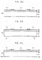
- Figure 1 is a perspective view illustrating one embodiment of an optical receiver using a variable optical attenuator according to the present invention
- Figure 2 is a plane view of an optical receiver using the variable optical attenuator
- Figure 3 is a sectional view of an optical receiver using the variable optical attenuator.
- the optical receiver using the variable optical attenuator includes a base member 100 formed in a predetermined shape; an input optical fiber 200 emitting an optical signal toward the base member 100; an optical receiving means 300 provided at one side of the base member 100, and receiving the optical signal; and a variable optical attenuator A actuated by an electrostatic force, changing a path of laser emitted from the input optical fiber 200, and thus adjusting optical power made to be incident to the optical receiving means 300.
- the base member 100 includes a plate portion 110 having a certain thickness and an area; an optical receiving means-mounted portion 120 at which the optical receiving means 300 is mounted, formed at one side of the plate portion 110 so as to have a certain area and a depth; a variable optical attenuator-mounted portion 130 at which the variable optical attenuator A is mounted, and formed at a side portion of the optical receiving means-mounted portion 120 so as to have a certain shape and a depth; and an optical path groove 140 making the optical receiving means-mounted portion 120 and the variable optical attenuator-mounted portion 130 communicating with each other, and through which laser is passes.
- the plate portion 110 is formed in a quadrangular form
- the optical receiving means-mounted portion 120 is formed in a quadrangular form with a certain depth.
- the variable optical attenuator-mounted portion 130 is formed in a quadrangular form with a certain depth, and its one side is opened.
- the optical path groove 140 has a certain width and a depth.
- the optical receiving means 300 includes a block 310 for fixing an optical diode, which is fixed to the base member 100; an optical diode provided with an optical diode active area 321 receiving laser, and mounted at the block 310 for fixing the optical diode.
- a lens for focusing laser may be mounted toward the active area 321 of the optical diode.
- the optical receiving means 300 is inserted at the optical receiving means-mounted portion 120 of the base member, and the lower portion of the optical receiving means 300 is soldered to be fixed at the optical receiving means-mounted portion 120 of the base member. At this time, the optical diode active area 321 is positioned at the optical path groove 140.
- variable optical attenuator A includes a substrate portion 400 having a certain area; an optical fiber-fixed portion 410 formed at one side of the substrate portion 400, and at which the input optical fiber 200 is fixed; a linear actuator part 420 formed on the substrate portion 400, and generating a linear actuation force by an electrostatic force; a body portion 430 isolated from the substrate portion 400, extended from one side of the linear actuator part 420, and moved by the linear actuator part 420; a micro mirror part 440 extended from one side of the body portion 430, and reflecting laser emitted from the input optical fiber 200 according to the movement of the body portion 430; and an elastically supporting portion 450 formed on the substrate portion 400, and elastically supporting the body portion 430.
- the substrate portion 400 has a quadrangular form, and its one side surface is stepped.
- the optical fiber-fixed portion 410 has a groove form with a certain depth, and is positioned at the higher portion of the substrate portion 400.
- the input optical fiber 200 is fixedly coupled with the optical fiber-fixed portion 410.
- a lens for focusing laser may be mounted.
- the optical fiber-fixed portion 410 is formed so that the input optical fiber 200 fixed at the optical fiber-fixed portion 410 is at a right angle to the optical receiving means 300.
- the linear actuator part 420 is a comb actuator which is generally used, and consists of a comb shaped fixed electrode 421 and a comb shaped movable electrode 422 inserted between the comb teeth of the fixed electrode 421.
- the body portion 420 has a predetermined shape, and is formed to be integral with the movable electrode 422 of the linear actuator part.
- the micro mirror part 440 is extended from one side of the body portion 430 and formed in a triangular form, and its one side surface becomes a reflection surface 441.
- the body portion 430 and the micro mirror part 440 are aligned so as to be collinear with the optical fiber-fixed portion 410.
- the reflection surface 441 of the micro mirror part is formed inclined at an angle of 45 to a path of laser emitted from the optical fiber 200.
- the elastically supporting portion 450 includes projections 451 formed on the substrate portion 400 and positioned at both sides of the body portion 430 respectively; and a plurality of leaf springs 452 connecting the projections 451 and the body portion 430.
- the leaf springs 452 are isolated from the substrate portion 400, and are positioned at both sides of the body portion 430 by two respectively.
- variable optical attenuator A Components of the variable optical attenuator A are integrally formed, and the variable optical attenuator whose components are integrally formed, is produced by a MEMS technology applying a lithographic technology and a micromachining technology).
- variable optical attenuator A In a state that the variable optical attenuator A has been inserted at the variable optical attenuator-mounted portion 130 of the base member, the variable optical attenuator A is soldered to the substrate portion 400 to be fixedly coupled with the base member 100.
- variable optical attenuator (A) In a state that the variable optical attenuator (A) is not in operation, when laser is emitted from an input optical fiber 200, the laser is reflected by the variable optical attenuator A, and then its entire optical power is made to be incident onto the optical receiving means 300.
- the variable optical attenuator A When the variable optical attenuator A is operated by an electrostatic force, a path of laser emitted from the input optical fiber 200 is changed, and thus a part of the optical power emitted from the input optical fiber 200 is made to be incident onto the optical receiving means 300.
- the input optical fiber 200, the micro mirror 440 part and the optical diode active area 321 are aligned so that, in an initial state that the power is not applied to a linear actuator part 420 of the variable optical attenuator, laser emitted from the input optical fiber 200 is reflected by the micro mirror part 44 and thus the entire optical power is made to be incident onto an optical diode active area 321. Accordingly, in a state that the linear actuator 420 is not in operation, the entire laser emitted from the input optical fiber 200 is made to be incident onto the optical diode active area 321.
- an optical receiving means-mounted portion 120 and a variable optical attenuator-mounted portion 130 are formed at the base plate 100.
- an optical receiving means 300 and a variable optical attenuator A are mounted respectively.
- the input optical fiber 200 is mounted.
- variable optical attenuator A since the components of the variable optical attenuator A are integrally formed, and the variable optical attenuator can be produced by a MEMS technology, it can be produced at a fine size. And, since the variable optical attenuator A is operated by an electrostatic force, it can be actuated at a high speed, and the power therefor is very small.
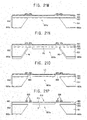
- Figure 7 is a perspective view illustrating another embodiment of an optical receiver provided with a modified base member and optical receiving member, which constitutes an optical receiver using a variable optical attenuator according to the present invention. The same number will be given to the same components as those described above in the drawing.
- a base member 100 of an optical receiver using the variable optical attenuator includes a plate portion 110 having a certain thickness and an area; a variable optical attenuator-mounted portion 130 formed at one side of the plate portion 110 so as to have a certain shape and depth, and at which the variable optical attenuator is mounted; and a fixed mirror part 460 formed at one side of the plate portion 110, and reflecting laser reflected by the variable optical attenuator to the optical receiving means 300 mounted at the plate portion 110.
- the fixed mirror part 460 may be implemented in various shapes, one embodiment thereof will now be described.
- An optical channel 461 with a certain width and a depth is formed at the plate portion 400 to communicate with the variable optical attenuator portion 130, and one side surface of the optical channel 461 is inclined, and becomes a reflection surface 462.
- variable optical attenuator A is mounted at the variable optical attenuator mounted portion 130, a structure thereof is the same as described above.
- an input optical fiber 200 from which laser is emitted is mounted.
- the optical receiving means 300 is an optical diode 320 having an active area 321, and the optical diode 320 is fixedly coupled with the base member 100 so that the active area 321 is positioned toward the fixed mirror part 460. At this time, the active area 321 of the optical diode is aligned so as to be collinear with the reflection surface 462 of the fixed mirror part.
- Figure 8 is a perspective view illustrating a first modified example of a variable optical attenuator according to the present invention.
- the variable optical attenuator includes substrate portion 500 having a certain area; an optical fiber fixed portion 510 at which the input optical fiber 200 is fixed, formed at one side of the substrate portion 500; a rotary actuator part 520 formed at the substrate portion, and generating an angular movement by an electrostatic force; a micro mirror part 530 extended from the rotary actuator part 520, and reflecting laser emitted from the input optical fiber 200 while making a angular movement according to the actuation of the rotary actuator part 520; and an elastically supporting portion 540 formed at the substrate portion 500, and elastically supporting the rotary actuator part 520.
- the substrate portion 500 is formed in a quadrangular form, and its one side surface is stepped.
- the optical fiber-fixed portion 510 has a certain depth, and is positioned at a higher portion of the substrate portion 500.
- the input optical fiber 200 is coupled with the optical fiber fixed-portion 510.
- the optical fiber-fixed portion 510 is formed so that the input optical fiber 200 fixed at the optical fiber-fixed portion 510 is at a right angle to the optical receiving means 300.
- the rotary actuator part 520 includes a fixed electrode 521 including a plurality of circular arc comb teeth 521 a formed in a circular arc form at a certain interval therebetween and an inclination type comb teeth 521 b connected with one side end of the circular arc comb teeth 521a; and a movable electrode 522 including circular arc teeth 522a movably positioned between the circular arc comb teeth 521a of the fixed electrode 521 and a connecting shaft 522b connected with the circular arc comb teeth 522a and with the micro mirror part 530.
- the rotary actuator part 520 is formed toward the lower portion of the substrate portion 500, and the movable electrode 522 is isolated from the substrate portion 500.
- the electrically supporting portion 540 includes a projection projected from the substrate portion 500, and a leaf spring 542 isolated from the substrate portion 500, and connected with an actuation side of the rotary actuator part 520, that is, the movable electrode 522.
- the leaf spring 542 is fixed at the projection 541, and elastically supporting the movable electrode 522.
- the micro mirror part 530 is extended from the connecting shaft 522b of the movable electrode in a triangular form, and its inclined surface becomes a reflection surface 531.
- the reflection surface 531 is formed inclined at an angle of 45 to a path of laser emitted from the input optical fiber 200.
- variable optical attenuator A Components of the variable optical attenuator A are integrally formed, and the variable optical attenuator A whose components are integrally formed is produced by a MEMS technology.
- the variable optical attenuator A is fixedly coupled with the variable optical attenuator-mounted portion 130.
- the input optical fiber200, the micro mirror part 530, and the optical diode active area 321 are aligned so that, in a state that the rotary actuator part 520 is not in operation, laser emitted from the input optical fiber 200 is reflected by the micro mirror part 530, and thus the entire optical power thereof is made to be incident to an optical diode active area 321. Therefore, in a state that the linear actuator part 520 is not in operation, the entire laser emitted from the input optical fiber 200 is made to be incident to the optical diode active area 321.
- the micro mirror part 530 makes an angular rotation by the operation of the rotary actuator part 520, the path of the laser reflected by the micro mirror part 530 is changed.
- the optical path is changed, and thus the optical power made to be incident to the active area 321 of the optical diode is adjusted.
- Figure 10 is a perspective view illustrating a second modified example of a variable optical attenuator according to the present invention.
- variable optical attenuator includes a substrate portion 600 having a certain area; an optical fiber-fixed portion 610 formed at one side of the substrate portion 600, and at which the input optical fiber 200 is fixed; a micro shutter part 620 movably positioned between the input optical fiber 200 and the optical diode 320 of the optical receiving means, and controlling that laser emitted from the input optical fiber 200 is introduced to the optical receiving means, that is, the active area 321 of the optical diode; an actuator part 630 moving the micro shutter part 620; and an elastically supporting portion 640 elastically supporting the micro shutter part 630.
- the substrate portion 600 is formed in a quadrangular form, and its one side surface is stepped.
- the optical fiber-fixed portion 610 is formed in a groove form having a certain depth.
- the optical fiber-fixed portion 610 is formed at a higher portion of the substrate portion 600 so as to be collinear with the optical receiving means 300 when the substrate portion 600 is mounted at the variable optical attenuator-mounted portion 130 of the base member.
- the actuator part 630 is a comb actuator, which is generally used, and consists of a comb-shaped fixed electrode 631 and a comb-shaped movable electrode 632 inserted between comb teeth of the fixed electrode 631. As described above, for the actuator part 630, the rotary actuator part may be used.
- the micro shutter part 620 is extended from the one side of the movable electrode 632 in a predetermined shape, and the longitudinal direction of the micro shutter part 620 is the same as the moving direction of the movable electrode 632.
- the micro shutter part 620 is isolated from the substrate portion 600 so as to be moved at a right angle to the direction of laser emitted from the input optical fiber 200 mounted at the optical fiber-fixed portion 610.
- the elastically supporting portion 640 consists of projections 641 formed on the substrate portion, and positioned at both sides of the micro shutter part 620 respectively; and a leaf spring 642 connecting the projections and the micro shutter part 620.
- the leaf spring 642 is isolated from the substrate portion 600.
- variable optical attenuator Components of the variable optical attenuator are integrally formed, and the variable optical attenuator is produced by a MEMS technology. And the variable optical attenuator is mounted at the variable optical attenuator-mounted portion 130 of the base member.
- the input optical fiber 200 is fixedly coupled with the optical fiber-fixed portion 610 of the variable optical attenuator. At this time, the input optical fiber 200 and the optical receiving means 300 are collinearly aligned.
- Figure 12 is a perspective view illustrating a third modified example of a variable optical attenuator according to the present invention.
- the variable optical attenuator includes a substrate portion 700 having a certain area; an optical fiber-fixed portion 710 formed at one side of the substrate portion 700, and at which the input optical fiber 200 is fixed; an incidence side mirror part 720 reflecting laser emitted from the input optical fiber 200; an emission side mirror part 730 reflecting laser reflected from the incidence side mirror part 720 to the optical receiving means 300; an actuator part 740 actuating the incidence side mirror part 720 or the emission side mirror part 730 and thus adjusting a reflection angle of laser reflected to the optical receiving means 300; and an elastically supporting portion 750 elastically supporting the incidence side mirror part 720 or the emission side mirror part 730 actuated by the actuator part 740.
- the substrate portion 700 is formed in a quadrangular form, and its one side surface is stepped.
- the optical fiber-fixed portion 710 is formed in a groove form with a certain depth.
- the optical fiber-fixed portion 710 is formed at a higher portion of the substrate portion 700 so as to be parallel to the optical receiving means 300 when the substrate portion 700 is mounted at the variable optical attenuator-mounted portion 130 of the base member.
- the optical receiving means 300 is an output optical fiber.
- the actuator part 740 is a comb actuator, which is generally used, and consists of a comb-shaped fixed electrode 741 and a comb shaped movable electrode 742 inserted between comb teeth of the fixed electrode 741.
- the incidence side mirror part 720 and the emission side mirror part 730 are integrally formed, and the incident side mirror part 720 and the emission side mirror part 730 which are integrally formed, are connected with the movable electrode 742 of the actuator part, and are isolated from the substrate portion 700.
- the elastically supporting portion 750 consists of a projection 751 projected from the substrate portion 700 and a leaf spring 752 isolated from the substrate portion 700 and elastically connecting the projection 751 and the incidence side mirror part 720. That is, one side of the incidence side mirror part 720 and the emission side mirror part 730, which are integrally formed, is elastically supported by the leaf spring 752.
- a reflection surface 721 of the incidence side mirror part is at a right angle to a reflection surface 731 of the emission side mirror part.
- FIG 13 a modified example for an incidence side mirror part 720, an emission side mirror part 730 and an elastically supporting portion 750 are illustrated.
- the emission side mirror part 730 is extended and projected from the substrate portion 700 in a quadrangular form, and the incidence side mirror part 720 is movably connected to a movable electrode 742 of the actuator part.
- a reflection surface 721 of the incidence side mirror part is at a right angle to a reflection surface 731 of the emission side mirror part.
- the elastically supporting portion 750 consists of a projection 751 formed on the substrate portion 700 and positioned at both sides of the incidence side mirror part 720 respectively and a leaf spring 752 connecting the incidence side mirror part 720 and the projection 751.
- the leaf spring 752 is isolated from the substrate portion 700, and elastically supports the incidence side mirror part 730.
- variable optical attenuator Components of the variable optical attenuator are integrally formed, and the variable optical attenuator is produced by a MEMS technology.
- the variable optical attenuator is mounted at the variable optical attenuator-mounted portion 130, the input optical fiber 200 is fixedly coupled with the optical fiber-fixed portion of the variable optical attenuator.
- variable optical attenuator having such structures will now be described with reference to Figures 14, 15.
- the actuator part 740 in a state that the actuator part 740 is not in operation, laser emitted from the input optical fiber 200 is reflected by the incidence side mirror part 720 and the emission side mirror part 730, and thus the entire optical power thereof is made to be incident to the optical receiving means 300, the output optical fiber. Therefore, in a state that the actuator part 740 is not in operation, the entire amount of the laser emitted from the input optical fiber 200 is made to be incident to the output optical fiber.
- Figure 16 is a perspective view illustrating a fourth modified example of a variable optical attenuator according to the present invention
- Figure 17 is a plane view of the variable optical attenuator
- Figure 18 is a sectional view of Figure 16.
- the variable optical attenuator includes a substrate portion 800 having a certain thickness and an area; a micro mirror part 810 positioned at the inside of the substrate portion 800 and reflecting laser emitted from the input optical fiber 200; a torsion hinge portion 820 connecting the micro mirror part 810 to the substrate portion 800 so that the micro mirror part 810 can makes a tilting actuation; and a piezoelectric actuator part 830 positioned at the substrate portion 800, having the micro mirror part 810 make a tilting rotation of the micro mirror part 810 by a piezoelectric actuation, and thus adjusting a reflection angle of laser reflected to the optical receiving means.
- the substrate portion 800 is formed in a quadrangular form, and the micro mirror part 810 having a quadrangular form is positioned in the middle of the substrate portion 800.
- the micro mirror part 810 is supported so as to make a tilting rotation by the torsion hinge portion 820.
- the torsion hinge portion 820 is positioned at both sides of the micro mirror part 810, and connects the micro mirror part 810 and the substrate portion 810.
- the micro mirror part 810 consists of a mirror plate 811 and a reflection film 812 coating the mirror plate 811.
- the piezoelectric actuator part 830 includes a capacitor area 831 encompassing one side of the micro mirror part 810, and an electrode area 832 extended from the one side of the capacitor area 831.
- the piezoelectric actuator part 830 is a piezoelectric material made of an upper thin plate, a piezoelectric material and a lower thin plate, and is adhered to one portion of the surface of the substrate portion 800.
- the capacitor area 831 is formed of an inner path 831 a and an outer path 831 b encompassing the inner path 831 a, and the inner path 831 a and the outer path 831b are connected to each other.
- the electrode area 832 has a lower electrode 832a formed of a lower thin plate and an upper electrode 832b formed of an upper plate, and the lower electrode 832a and the upper electrode 832b are isolated from each other.
- a dummy actuator part 840 On the basis of a central line of the micro mirror part 810, that is, on the basis of the torsion hinge portions 820, on the opposite side of the piezoelectric actuator part 830, a dummy actuator part 840 having the same shape as the piezoelectric actuator part 830 is provided.
- the dummy actuator part 840 offsets a residual stress of the micro mirror part 810.
- variable optical attenuator Components of the variable optical attenuator are integrally formed, and the variable optical attenuator is produced by a MEMS technology.
- the variable optical attenuator is vertically mounted at the variable optical attenuator-mounted portion 130 of the base member, an input optical fiber 200 and an output optical fiber which is an optical receiving means 300 are fixedly mounted at the base member 100 so as to be at a certain inclination angle to the micro mirror part 810.
- the input optical fiber 200 and the output optical fiber are fixedly coupled so as to be symmetrical on the basis of a virtual axis, which is at a right angle to a reflection surface 812 of the micro mirror part 810.
- Figures 21a to 21p are sectional views illustrating one embodiment of a method for producing the variable optical attenuator in a producing order respectively. And, the same number will be given to the same components as those in Figures 16, 17 and 18.
- a substrate, a silicon wafer with a certain thickness onto which an embedded insulated film layer and a silicon thin film layer are formed is made as a raw material, and at front and back surfaces of the substrate 850, a low-stress insulated thin film layer 860 is patterned.
- a low-stress silicon nitride film whose residual stress is minimized may be used.
- the upper silicon thin film layer 853 reduces a transformation of a mirror surface, and is used to form a mirror plate 811 for restraining a micro mirror part 810 from being transformed in proportion to a stress applied thereto by a piezoelectric actuator part 830 in operation of the micro mirror part 810. Therefore, as adjusting the thickness of the upper silicon thin film layer 853, a thickness of the micro mirror part 810 is adjusted.
- a lower electrode (L1) formed of Pt or the like, a piezoelectric material (L2) formed of PZT or the like and an upper electrode (L3) formed of Pt, RuO2 or the like are laminated in a thin film form with a predetermined thickness.
- a material for a hard mask (M1) layer is patterned on the upper electrode (L3), and a photoresist film layer (P1) is spin-coated thereon, and then, is patterned using a photolithography process.
- the material for the hard mask (M1) will function as an etching mask in fabricating the piezoelectric capacity.
- a thin film layer for a piezoelectric material etching mask exposed through the photoresist film shape is eliminated using the methods of dry etching, wet chemical etching or the like. Then, by eliminating the photoresist film layer remaining on the substrate surface, a piezoelectric material capacitor etching mask (M2) is patterned.
- a shape of a piezoelectric material capacitor etching mask (M2) is fabricated.
- a photoresist film layer (P2) to be used as an etching mask for eliminating a portion (A1 ) of a low-stress insulated thin film layer 860 where a micro mirror part 810 will be formed, is patterned by a photolithography process.
- the exposed area of the low-stress insulated thin film layer 860 is defined so that a predetermined area of the silicon thin film layer 853 where a flat reflection surface 812 will be formed is defined. Then, the exposed low-stress insulated thin film layer 860 is eliminated, and the photoresist film layer (P2) is eliminated too.
- a photoresist film layer (P3) is spin-coated and patterned by a photolithography process.
- a metal thin film layer L4 for patterning a mirror reflection film layer formed of gold, aluminum or the like for providing a mirror surface with a high reflectivity is deposited.
- the micro mirror part reflection film layer 812 is patterned.
- P4 photoresist film
- the release process is that a slit line 833 is formed at the substrate so as to form a piezoelectric actuator part and a torsion hinge portion 820, that is, one portion of the substrate is eliminated, so that the micro mirror part 810 suspended at portions of the torsion hinge portion 820 and the piezoelectric actuator part 830, can freely moved.
- the metal thin film layer (L5) for the etching hard mask, which is exposed through the photoresist film layer (P4) is eliminated by one of wet etching and dry etching such as reactive ion etching and thus a release etching mask (L5-1) is patterned at an upper surface of the substrate in advance.
- a photoresist film layer (P5) is patterned by a photolithography process at a lower surface of the low-stress insulated thin film layer 860 formed at the silicon wafer 851 of the substrate.
- the low-stress insulated thin film layer 860 which is exposed through the photoresist film layer (P5) is etched until the silicon wafer 851 is exposed, and the remaining photoresist film layer is eliminated, so that a mask 860a for etching the silicon wafer is patterned.
- an upper surface of the substrate where the piezoelectric material or the like is patterned is protected, and the silicon wafer 851 which is exposed through the mask pattern for etching the lower portion thereof is etched in alkali aqueou solution such as KOH (potassium hydroxide), EDP (ethylenediamine), TMAH (tetramethyl ammonium hydroxide) or the like, so that a cavity 851 a is formed.
- alkali aqueou solution such as KOH (potassium hydroxide), EDP (ethylenediamine), TMAH (tetramethyl ammonium hydroxide) or the like.
- a photoresist film layer is spin-coated to the inside of the etched cavity 851 a and a lower surface of the substrate 850, and a photoresist film layer (P6) for an mirror plate etching mask is patterned by a photolithography technology.
- the embedded insulated film layer 852 and the silicon thin film layer 853 which are exposed through the photoresist film layer (P6), are etched from the lower portion of the substrate 850 and eliminated, and the low-stress insulated thin film layer 860 of the substrate surface is exposed. Then, the remaining photoresist film layer is eliminated.
- portions of the micro mirror part 810, the piezoelectric actuator part 830 having a cantilever form, the torsion hinge portion 820 and the like suspend from a portion of the substrate 850.
- a plurality of completed piezoelectric actuator micro mirror devices passed through the process above, that is a variable optical attenuator devices are isolated into an individual device using a dicing process, and an optical axis of each optical attenuator device, input optical fiber 200 and output optical fiber is aligned so that the three of them are at a predetermined angle. In this way, the components are assembled in a package thereby implementing an optical receiver.
- a lens which can focus laser may be added between input/output optical fibers and the micro mirror part, or the function of lens may be added to the input and output optical fibers.
- an optical fiber-fixed portion that makes the input/output optical fibers symmetrically aligned at a predetermined angle on the basis of a virtual axis which is at a right angle to a reflection surface of a piezoelectric actuation micro mirror part, may be included.
- variable optical attenuator and an optical receiver having the variable optical attenuator as a component therefor can be extremely finely produced, a unit cost in producing is inexpensive, and the variable optical attenuator or the optical receiver using the variable optical attenuator can be mass-produced.
- an optical transmitter using a variable optical attenuator includes a base member 100 formed in a predetermined shape; an optical diode 320 mounted at one side of the base member 100, and emitting an optical signal; an output optical fiber 340 mounted at one side of the base member 100, and receiving an optical signal; and a variable optical attenuator A actuated by an electrostatic force, changing a path of laser emitted from the optical diode 320, and thus adjusting optical power transmitted to the output optical fiber 340.
- the base member 100 includes an variable optical attenuator-mounted portion 130 formed at one side of a plate portion 110 having a quadrangular form with a certain thickness, and at which the variable optical attenuator is mounted; a diode-mounted portion 150 formed at a side portion of the variable optical attenuator-mounted portion 130, and at which the optical diode 320 is mounted; and an optical fiber-fixed portion 160 formed at a side portion of the variable optical attenuator-mounted portion 130, and at which the output optical fiber 340 is mounted.
- the diode-mounted portion 150 is formed in a quadrangular form having a certain depth.
- the variable optical attenuator-mounted portion 130 is formed in a quadrangular form having a certain depth, and one side thereof is opened.
- the optical fiber-fixed portion 160 is formed in a penetrated form having a certain width and a depth, and is positioned at a right angle to the diode-mounted portion 150.
- the variable optical attenuator A includes a substrate portion 900 having a certain thickness and an area; a linear actuator part 910 formed at the substrate portion 900, and generating a linear actuation force by an electrostatic force; a body portion 920 isolated from the substrate portion 900, extended from one side of the linear actuator part 910, and moved by the linear actuator part 910; a micro mirror part 930 extended from one side of the body portion 920, and reflecting laser emitted from the optical diode 320 according to a movement of the body portion 920; and an elastically supporting portion formed at the substrate portion 900, and elastically supporting the body portion 920.
- variable optical attenuator A Components of the variable optical attenuator A are integrally formed, and the variable optical attenuator A whose components are integrally formed is produced by a MEMS technology.
- variable optical attenuator A is fixedly coupled with the variable optical attenuator-mounted portion 130 of the base member
- the output optical fiber 340 is fixedly coupled with the optical fiber-fixed portion 160 of the base member
- the optical diode 320 is fixedly coupled with the diode-mounted portion 150 of the base member.
- variable optical attenuator A In a state that the variable optical attenuator A is not in operation, when an optical signal is transmitted from the optical diode 320, the optical signal is reflected by the variable optical attenuator A, and thus the entire optical power is transmitted to the output optical fiber 340. And, when the linear actuator part 910 of the variable optical attenuator is operated by an electrostatic force, while an optical path of the optical signal transmitted from the optical diode 320 is changed and is made to be incident to the output optical fiber 340, a part of optical power transmitted from the optical diode 320 is transmitted to the output optical fiber 340. That is, a path of laser emitted from the optical diode 320 by the operation of the variable optical attenuator A is changed and transmitted to the output optical fiber 340 thereby adjusting emitted optical power.
- An optical receiver using a variable optical attenuator may be implemented into a multi type optical receiver.
- the multi type optical receiver is that an optical receiver using the variable optical attenuator is made as one unit, and a plurality of units is aligned.
- an optical transmitter using a variable optical attenuator may be implemented into multi type optical transmitter in the same manner as the multi type optical receiver.
- variable optical attenuator components constituting a variable optical attenuator for attenuating laser are integrally formed, and the variable optical attenuator whose components are integrally formed can be produced at a fine size by a MEMS technology whereby the size thereof is extremely small, and mass production thereof is possible. Therefore a unit cost can be remarkably in producing the variable optical attenuator, the variable optical attenuator is actuated with a small electric energy thereby reducing consumed electric power.
- the attenuator can be actuated at a high-speed thereby remarkably reducing wave length and polarization dependency, so that it can be minimized that a signal is distorted in a long-distance optical fiber network.
- variable optical attenuator can be applied to a various devices such as an optical output controller, an optical signal adjusting multiplexer, an optical signal connector or the like on an optical network adopting a wave division multiplexing method.
Landscapes
- Physics & Mathematics (AREA)
- General Physics & Mathematics (AREA)
- Optics & Photonics (AREA)
- Mechanical Light Control Or Optical Switches (AREA)
- Optical Couplings Of Light Guides (AREA)
- Micromachines (AREA)
Applications Claiming Priority (6)
| Application Number | Priority Date | Filing Date | Title |
|---|---|---|---|
| KR1020020074096A KR20040046253A (ko) | 2002-11-26 | 2002-11-26 | 압전 구동 가변 광 감쇠기 및 제조 방법 |
| KR2002074096 | 2002-11-26 | ||
| KR2003025458 | 2003-04-22 | ||
| KR10-2003-0025458A KR100492544B1 (ko) | 2003-04-22 | 2003-04-22 | 광감쇠기 일체형 광 수신기 및 광 송신기 |
| KR1020030026464A KR20040092227A (ko) | 2003-04-25 | 2003-04-25 | 광감쇠기 |
| KR2003026464 | 2003-04-25 |
Publications (2)
| Publication Number | Publication Date |
|---|---|
| EP1424583A2 true EP1424583A2 (de) | 2004-06-02 |
| EP1424583A3 EP1424583A3 (de) | 2004-06-09 |
Family
ID=32303324
Family Applications (1)
| Application Number | Title | Priority Date | Filing Date |
|---|---|---|---|
| EP03026635A Withdrawn EP1424583A3 (de) | 2002-11-26 | 2003-11-19 | Optischer Empfänger und optischer Sender mit variablem optischem Dämpfungsglied, Herstellungsverfahren für ein variables optisches Dämpfungsglied |
Country Status (3)
| Country | Link |
|---|---|
| US (1) | US20040114942A1 (de) |
| EP (1) | EP1424583A3 (de) |
| JP (1) | JP2004310029A (de) |
Cited By (1)
| Publication number | Priority date | Publication date | Assignee | Title |
|---|---|---|---|---|
| CN102882607A (zh) * | 2012-09-10 | 2013-01-16 | 青岛海信宽带多媒体技术有限公司 | 光模块及调节光模块接收光功率的方法 |
Families Citing this family (20)
| Publication number | Priority date | Publication date | Assignee | Title |
|---|---|---|---|---|
| WO2005040036A1 (en) * | 2003-10-27 | 2005-05-06 | Bookham Technology Plc | Optical assembly with variable optical attenuator |
| FR2880731B1 (fr) * | 2005-01-11 | 2007-04-27 | Commissariat Energie Atomique | Composant, notamment avec des elements actifs, et procede de realisation d'un tel composant |
| JP5092406B2 (ja) * | 2007-01-10 | 2012-12-05 | セイコーエプソン株式会社 | アクチュエータ、光スキャナおよび画像形成装置 |
| JP2009014768A (ja) * | 2007-06-29 | 2009-01-22 | Fujitsu Ltd | メムスデバイスおよびその製造方法 |
| JP5252687B2 (ja) * | 2008-01-18 | 2013-07-31 | スタンレー電気株式会社 | 光偏向器 |
| JP4908468B2 (ja) * | 2008-03-10 | 2012-04-04 | 日本電信電話株式会社 | 可変光減衰器を内蔵した光受信器 |
| JP2011180534A (ja) * | 2010-03-03 | 2011-09-15 | Furukawa Electric Co Ltd:The | Mems素子、可動式ミラー、および光スイッチ装置 |
| US9473300B2 (en) * | 2011-11-03 | 2016-10-18 | Savannah River Nuclear Solutions, Llc | Authenticated sensor interface device |
| JP2014187506A (ja) * | 2013-03-22 | 2014-10-02 | Sumitomo Electric Ind Ltd | 光受信器及びその製造方法 |
| DE102013209238B4 (de) * | 2013-05-17 | 2017-10-12 | Fraunhofer-Gesellschaft zur Förderung der angewandten Forschung e.V. | MEMS-Struktur und Verfahren zum Herstellen derselben |
| JP6495640B2 (ja) | 2014-12-11 | 2019-04-03 | 日本オクラロ株式会社 | 光通信装置、及び光通信装置の製造方法 |
| JP2016143018A (ja) * | 2015-02-05 | 2016-08-08 | ソニー株式会社 | 光送信装置、光受信装置、及び光ケーブル |
| JP6645078B2 (ja) * | 2015-09-03 | 2020-02-12 | 株式会社リコー | 光偏向器及び光走査装置 |
| JP6578191B2 (ja) * | 2015-11-18 | 2019-09-18 | 日本ルメンタム株式会社 | 光モジュール及び光モジュールの製造方法 |
| JP6783134B2 (ja) | 2016-12-13 | 2020-11-11 | 日本ルメンタム株式会社 | 光モジュール及び光モジュールの製造方法 |
| CN110692170B (zh) * | 2017-02-01 | 2022-06-24 | 光互通控股有限公司 | 连接器接合感测机构 |
| WO2018220847A1 (ja) * | 2017-06-02 | 2018-12-06 | オリンパス株式会社 | 光量検知装置 |
| CN115657296A (zh) * | 2017-11-15 | 2023-01-31 | 浜松光子学株式会社 | 光学器件的制造方法 |
| CN109932782B (zh) * | 2019-04-11 | 2020-11-27 | 北京理工大学 | 一种基于电热驱动式微镜的硅基moems光开关装置 |
| CN119560884A (zh) * | 2024-11-19 | 2025-03-04 | 江苏奥雷光电有限公司 | 集成光学衰减功能的激光器组件 |
Family Cites Families (8)
| Publication number | Priority date | Publication date | Assignee | Title |
|---|---|---|---|---|
| BE364836A (de) * | ||||
| GB0020427D0 (en) * | 2000-08-18 | 2000-10-04 | Kymata Ltd | Moem device and fabrication method |
| JP2002116389A (ja) * | 2000-10-04 | 2002-04-19 | Furukawa Electric Co Ltd:The | 可変光減衰器 |
| JP2002221676A (ja) * | 2001-01-25 | 2002-08-09 | Furukawa Electric Co Ltd:The | 可変光減衰器 |
| WO2002086602A1 (en) * | 2001-04-17 | 2002-10-31 | M2N, Inc. | Micro-actuator and micro-device using the same |
| US6751395B1 (en) * | 2001-11-09 | 2004-06-15 | Active Optical Networks, Inc. | Micro-electro-mechanical variable optical attenuator |
| US6856749B2 (en) * | 2002-10-10 | 2005-02-15 | Fitel Technologies, Inc. | Optical coupling and alignment device |
| US20040136680A1 (en) * | 2003-01-09 | 2004-07-15 | Teraop Ltd. | Single layer MEMS based variable optical attenuator with transparent shutter |
-
2003
- 2003-11-19 EP EP03026635A patent/EP1424583A3/de not_active Withdrawn
- 2003-11-20 JP JP2003390780A patent/JP2004310029A/ja not_active Withdrawn
- 2003-11-24 US US10/718,806 patent/US20040114942A1/en not_active Abandoned
Cited By (1)
| Publication number | Priority date | Publication date | Assignee | Title |
|---|---|---|---|---|
| CN102882607A (zh) * | 2012-09-10 | 2013-01-16 | 青岛海信宽带多媒体技术有限公司 | 光模块及调节光模块接收光功率的方法 |
Also Published As
| Publication number | Publication date |
|---|---|
| JP2004310029A (ja) | 2004-11-04 |
| EP1424583A3 (de) | 2004-06-09 |
| US20040114942A1 (en) | 2004-06-17 |
Similar Documents
| Publication | Publication Date | Title |
|---|---|---|
| EP1424583A2 (de) | Optischer Empfänger und optischer Sender mit variablem optischem Dämpfungsglied, Herstellungsverfahren für ein variables optisches Dämpfungsglied | |
| Wu | Micromachining for optical and optoelectronic systems | |
| US6360033B1 (en) | Optical switch incorporating therein shallow arch leaf springs | |
| US6526198B1 (en) | Micromachined optomechanical switches | |
| CN113960561A (zh) | 具有单片阵列的激光雷达模块 | |
| WO2003062899A1 (en) | Optical switch and production method therefor, information transmission device using it | |
| JP2003014997A (ja) | 超小型光電子機械システム(moems) | |
| JP2005505000A (ja) | ビームステアリング光スイッチング素子 | |
| KR20010102533A (ko) | 캔틸레버형 마이크로구조 장치 및 그 제조 방법 | |
| US20060280421A1 (en) | Variable light attenuator | |
| EP2976292B1 (de) | Integrierter mikrospiegel mit öffnung und anwendungen davon | |
| CN113885125A (zh) | 平面内mems光开关 | |
| CN113885122A (zh) | 具有停止控件的mems光开关 | |
| KR100473491B1 (ko) | 가변 광감쇠기 및 이의 제조방법 | |
| CN113885123A (zh) | 具有悬臂耦合器的mems光开关 | |
| US20030012545A1 (en) | Broad-band variable optical attenuator | |
| US6961488B2 (en) | Optical switch and method of producing the same | |
| CN113885126A (zh) | 用于光耦合的mems开关 | |
| KR20030057681A (ko) | 광 스위치 및 그 제조 방법 | |
| KR20040072406A (ko) | 파장 조절 광 공진기 및 그를 이용한 튜너블 광 필터 | |
| JP5301875B2 (ja) | 可変光減衰器および可変光減衰器搭載光送受信器 | |
| JP4177051B2 (ja) | 可変光減衰器及び光部品 | |
| Hashimoto et al. | Micro-optical gate for fiber optic communication | |
| JPWO2002103432A1 (ja) | 光スイッチ | |
| US20050078932A1 (en) | Variable optical attenuator |
Legal Events
| Date | Code | Title | Description |
|---|---|---|---|
| PUAI | Public reference made under article 153(3) epc to a published international application that has entered the european phase |
Free format text: ORIGINAL CODE: 0009012 |
|
| PUAL | Search report despatched |
Free format text: ORIGINAL CODE: 0009013 |
|
| AK | Designated contracting states |
Kind code of ref document: A2 Designated state(s): AT BE BG CH CY CZ DE DK EE ES FI FR GB GR HU IE IT LI LU MC NL PT RO SE SI SK TR |
|
| AX | Request for extension of the european patent |
Extension state: AL LT LV MK |
|
| AK | Designated contracting states |
Kind code of ref document: A3 Designated state(s): AT BE BG CH CY CZ DE DK EE ES FI FR GB GR HU IE IT LI LU MC NL PT RO SE SI SK TR |
|
| AX | Request for extension of the european patent |
Extension state: AL LT LV MK |
|
| RIC1 | Information provided on ipc code assigned before grant |
Ipc: 7G 02B 6/26 B Ipc: 7B 81B 3/00 B Ipc: 7G 02B 6/43 B Ipc: 7G 02B 26/02 A |
|
| RIN1 | Information on inventor provided before grant (corrected) |
Inventor name: BU, JONG-UK Inventor name: SONG, KI-CHANG Inventor name: LIM, TAE-SUN Inventor name: JI, CHANG-HYEON Inventor name: YEE, YOUNG-JOO |
|
| 17P | Request for examination filed |
Effective date: 20041002 |
|
| AKX | Designation fees paid |
Designated state(s): AT BE BG CH CY CZ DE DK EE ES FI FR GB GR HU IE IT LI LU MC NL PT RO SE SI SK TR |
|
| 17Q | First examination report despatched |
Effective date: 20050228 |
|
| 17Q | First examination report despatched |
Effective date: 20050228 |
|
| STAA | Information on the status of an ep patent application or granted ep patent |
Free format text: STATUS: THE APPLICATION IS DEEMED TO BE WITHDRAWN |
|
| 18D | Application deemed to be withdrawn |
Effective date: 20061110 |