EP1416510A2 - Panneau à décharge gazeuse et procédé de production de celui-ci - Google Patents
Panneau à décharge gazeuse et procédé de production de celui-ci Download PDFInfo
- Publication number
- EP1416510A2 EP1416510A2 EP20030256366 EP03256366A EP1416510A2 EP 1416510 A2 EP1416510 A2 EP 1416510A2 EP 20030256366 EP20030256366 EP 20030256366 EP 03256366 A EP03256366 A EP 03256366A EP 1416510 A2 EP1416510 A2 EP 1416510A2
- Authority
- EP
- European Patent Office
- Prior art keywords
- protective film
- driving voltage
- gas discharge
- reducing compound
- discharge panel
- Prior art date
- Legal status (The legal status is an assumption and is not a legal conclusion. Google has not performed a legal analysis and makes no representation as to the accuracy of the status listed.)
- Withdrawn
Links
Images


Classifications
-
- H—ELECTRICITY
- H01—ELECTRIC ELEMENTS
- H01J—ELECTRIC DISCHARGE TUBES OR DISCHARGE LAMPS
- H01J11/00—Gas-filled discharge tubes with alternating current induction of the discharge, e.g. alternating current plasma display panels [AC-PDP]; Gas-filled discharge tubes without any main electrode inside the vessel; Gas-filled discharge tubes with at least one main electrode outside the vessel
- H01J11/10—AC-PDPs with at least one main electrode being out of contact with the plasma
- H01J11/12—AC-PDPs with at least one main electrode being out of contact with the plasma with main electrodes provided on both sides of the discharge space
-
- H—ELECTRICITY
- H01—ELECTRIC ELEMENTS
- H01J—ELECTRIC DISCHARGE TUBES OR DISCHARGE LAMPS
- H01J11/00—Gas-filled discharge tubes with alternating current induction of the discharge, e.g. alternating current plasma display panels [AC-PDP]; Gas-filled discharge tubes without any main electrode inside the vessel; Gas-filled discharge tubes with at least one main electrode outside the vessel
- H01J11/20—Constructional details
- H01J11/34—Vessels, containers or parts thereof, e.g. substrates
- H01J11/40—Layers for protecting or enhancing the electron emission, e.g. MgO layers
-
- H—ELECTRICITY
- H01—ELECTRIC ELEMENTS
- H01J—ELECTRIC DISCHARGE TUBES OR DISCHARGE LAMPS
- H01J9/00—Apparatus or processes specially adapted for the manufacture, installation, removal, maintenance of electric discharge tubes, discharge lamps, or parts thereof; Recovery of material from discharge tubes or lamps
- H01J9/02—Manufacture of electrodes or electrode systems
Definitions
- the present invention relates to a gas discharge panel and a production method thereof. More specifically, the present invention relates to a method of producing a gas discharge panel for a plasma display panel (PDP) or a plasma addressing liquid crystal device (PALC), for example.
- the gas discharge panel according to the present invention is desirably used in household TVs and computer monitors, as well as in large-screen displays for displaying information installed at stations, airports, stock exchanges, factories, schools and the like.
- PDP plasma display panels
- PLC plasma addressing liquid crystal devices
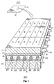
- FIG. 1 is a schematic perspective view illustrating the internal structure of the PDP.
- a PDP 100 depicted in Fig. 1 generally consists of a front side substrate and a back side substrate.
- the front side substrate generally consists of a plurality of display electrodes in the form of strips (plural lines of electrodes) formed on a glass substrate 11, a dielectric layer 17 formed so as to cover the display electrodes, and a protective film (for example, an MgO layer) 18 formed on the dielectric layer 17 and exposed to a discharge space.
- a protective film for example, an MgO layer
- Each display electrode consists of a transparent electrode film 41 in the form of a strip or stripe and a bus electrode 42 laminated on the transparent electrode film 41.
- the bus electrode 42 is also formed as a strip or stripe and is narrower in width than the transparent electrode film strip.
- the back side substrate generally consists of a plurality of address electrodes A in the form of strips (stripes) formed on a glass substrate 21, a plurality of barrier ribs 29 in the form of strips formed on the glass substrate 21 between neighboring address electrodes, and a phosphor layer 28 formed between barrier ribs 29 including between the barrier ribs and wall surfaces.
- a phosphor material for use in the phosphor layer (Y, Gd)BO 3 :Eu for red, Zn 2 SiO 4 :Mn for green, and BaMgAl 10 O 17 :Eu for blue are exemplified.
- R, G and B respectively represent unit light-emitting areas of red, green and blue, and constitute pixels by laterally arranging RGB areas.
- the front side substrate manufacturing process comprises the steps of: forming the transparent electrode film (into strips) on the substrate, forming the bus electrodes, forming the dielectric layer, and forming the protective film.
- the back side substrate manufacturing process comprises the steps of: forming the address electrodes on the substrate, forming the barrier ribs, and forming the phosphor layer.
- the front side substrate and the back side substrate thus obtained through the front side substrate manufacturing process and the back side substrate manufacturing process are then subjected to a panel assembling step, intra-panel evacuation step, and intra-panel discharge gas introducing step, to complete the PDP.
- a gas discharge panel having at least a protective film containing a driving voltage-reducing compound.
- a method of producing a gas discharge panel including the step of forming a protective film containing a driving voltage-reducing compound by exposing a protective film to an atmosphere of driving voltage-reducing compound directly after formation of the protective film.
- a method of producing a gas discharge panel including the step of exposing a protective film to an atmosphere of driving voltage-reducing compound after irradiating the protective film with vacuum UV rays, thereby forming a protective film containing a driving voltage-reducing compound.
- a method of producing a gas discharge panel including the steps of heating a protective film to 300°C or more, cooling the same to atmospheric temperature, and then exposing the protective film to an atmosphere of driving voltage-reducing compound, thereby forming a protective film containing a driving voltage-reducing compound.
- a gas discharge panel of the first aspect of the present invention contains a protective film containing a driving voltage-reducing compound.
- gas discharge panel refers, but is not limited, to any panels which achieve display using gas discharge, for example PDP, PALC and the like.
- the driving voltage-reducing compound is not particularly limited insofar as it can reduce driving voltage by being contained in the protective film.
- driving voltage-reducing compounds include inorganic compounds such as hydrogen and carbon monoxide; hydrocarbons such as methane, ethane, propane, butane, ethylene, acetylene, vinylacetylene, methoxyacetylene, ethoxyacetylene, propylene, propine, allene, 2-methylpropene, isobutane, 1-butene, 2-butene, 1,3-butadiene, 1,2-butadiene, 1,3-butadiyne, bicycle[1.1.0]-butane, 1-butyne, 2-butyne, cyclopropane, cyclobutane and cyclobutene; ethers such as dimethyl ether, diethyl ether, ethylmethyl ether, methylvinyl ether, divinyl ether, diethylene glycol monobutyl ether, 1,4-dioxine, diethylene glycol monobutyl ether acetate and furan; alcohols such as
- 1-propanol diethylene glycol monobutyl ether acetate, methane, ⁇ -terpineol and 1-butanol are preferably used.
- the content ratio of the driving voltage-reducing compound is preferably, but not particularly limited insofar as it can reduce the driving voltage, in the range of 0.1 to 2.0% by weight with respect to the protective film. Content ratios of less than 0.1% by weight are not preferred because sufficient effect cannot then be achieved, whilst content ratios of more than 2.0% by weight are not preferred because the compound may emit gas during electric discharge, thus hindering the electric discharge if too much compound is present. A still more preferable content ratio is in the range of 0.6 to 1.0% by weight.
- the mechanism by which the above compound reduces the driving voltage is not clearly known, it is believed that by incorporating the above compound in the protective film, the conductive state of the protective film or the discharge rate of secondary electrons changes, which results in reduction of driving voltage. More specifically, by containing the above compound, it is possible to reduce the driving voltage by 10V or more (for example, 10 to 20 V) compared to the case where the compound is not present.
- the protective film is usually formed of a MgO film, however, an SrO film may also be used.
- any known methods can be used without any limitation. For example, physical deposition methods such as vapor deposition, and applying and baking methods and the like can be used.
- the thickness of the protective film is preferably in the range of 0.5 to 1.5 ⁇ m.
- a three electrode AC-type surface discharge PDP shown in Fig. 1 will be described below. It is to be noted that the following examples are provided only for illustration and are not limiting to the scope of the present invention.
- a PDP 100 shown in Fig. 1 consists of a front side substrate and a back side substrate.
- the front side substrate generally consists of strips of display electrodes (a plurality of lines or stripes) formed on a glass substrate 11, a dielectric layer 17 formed so as to cover the display electrodes, and a protective film 18 formed on the dielectric layer 17 and exposed to a discharge space.
- the driving voltage reducing compound is applicable to the above protective film 18.
- the display electrodes are comprised from a transparent electrode film 41 in the form of strips (stripes) or dots per discharge cell unit, and from bus electrodes 42 laminated on the transparent electrode film 41 for reducing the resistance of the transparent electrode film.
- the bus electrodes 42 are in the form of strips (stripes) and each strip is narrower in width than that of the corresponding transparent electrode film strip.
- the method of forming the transparent electrode film 41 a forming method which involves application of a paste containing an organic compound of a metal constituting the transparent electrode film and baking of the same is exemplified.
- the back side substrate generally consists of a plurality of address electrodes A in the form of strips (stripes) formed on the glass substrate 21, a plurality of barrier ribs 29 in the form of strips (stripes) formed on the glass substrate 21 between neighboring address electrodes, and a phosphor layer 28 formed between barrier ribs 29 including between the ribs and the wall faces.
- the barrier ribs 29 can be formed by applying a paste containing low-melting glass and a binder on the dielectric layer 27 so as to form a film, baking the film, and cutting the film using a mask in the shape of barrier ribs by means of a sandblast method.
- a photosensitive resin used for the binder, it may be formed by baking after exposure and development using a mask of a predetermined shape.
- the phosphor layer 28 can be formed by applying a paste in which a granular phosphor material is dispersed in a solution dissolving the binder, between the barrier ribs 29, and baking the same in an inert atmosphere.
- the driving voltage-reducing compound includes a reductive compound
- the compound may reduce the phosphor material (thus deteriorating it) during production process and driving. For this reason, it is preferred to use an anti-reducing substance for the phosphor material.
- BaAl 12 O 19 :Mn (green), Y 2 SiO 5 :Ce (blue) and the like can be used.
- the dielectric layer may be formed on the glass substrate 21 so as to cover the address electrodes A, and the barrier ribs and the phosphor layer may be formed on the dielectric layer.
- the above front side substrate and the back side substrate are aligned opposite each other with their inner faces opposing so that the display electrodes and the address electrodes intersect at right angles, and spaces surrounded (enclosed) by the barrier ribs 29 are filled with a discharge gas, to thereby form the PDP 100.
- the PDP which may be used in the present method is not limited to the PDP having the above structure shown in Fig. 1, but any PDP can be used insofar as it has a protective film, such as of opposite discharge type, or transparent type in which a phosphor layer is arranged on the front side substrate, as well as a PDP having a two electrode structure. Additionally, the barrier ribs may be of a mesh form.
- the expression “directly after” refers to the period during which the active part of the protective film still exists (i.e. is not substantially reduced).
- the protective film by irradiating with vacuum UV rays.
- the irradiation is preferably performed under the conditions: vacuum UV rays having a wavelength of 120 to 300 nm, 0.5 to 50 mW/cm 3 in energy, for 5 to 10 minutes. The shorter the wavelength, the better the efficiency.
- the method (3) it is possible to activate the protective film by heating the protective film. Furthermore, by exposing the protective film to the atmosphere of driving voltage-reducing compound after cooling the same to atmospheric temperature, it is possible to efficiently contain the compound in the protective film. If the protective film is exposed to the atmosphere of the compound without first being cooled, it is impossible to efficiently contain (introduce or adsorb) the compound because the compound is highly active.
- the time interval for exposing to the atmosphere of driving voltage-reducing compound is usually from 10 minutes to 1 hour depending on the compound being used.
- Japanese Unexamined Patent Publication No. HEI 9(1997) -92161 discloses, for improving the lifetime of a PDP, a method of mixing 0.0001 to 1% of reductive gas in the discharge gas. Although this method improves the life of PDP by removing oxygen remaining in the discharge space, there is no description with regard to modification of the protective film, and hence it is different from the aspects of the present invention.
- Japanese Unexamined Patent Publication No. HEI 3(1991) -230447 discloses a method of reducing the ageing time by removing excess oxygen in the protective film by input/output of reductive gas, and thereby stabilizing the oxidation state of the protective film. Practically, input/output of reductive gas is conducted at high temperature of 360°C, and in such high temperature condition, the reductive gas will not adsorb to the protective film.
- the above patent is different in this respect from the aspects of the present invention.
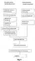
- FIG. 3 is similar to Fig. 2 which is the conventional process flow chart, except that a step of exposing the protective film to an atmosphere of driving voltage-reducing compound is further included and BaAl 12 O 19 : Mn having high reduction resistance is used as a green phosphor material.
- a step of exposing the protective film to an atmosphere of driving voltage-reducing compound is further included and BaAl 12 O 19 : Mn having high reduction resistance is used as a green phosphor material.
- a transparent electrode film 41 in the form of striped plural lines is formed on a glass substrate 11 by a known method (transparent conductive film forming step).
- bus electrodes 42 are formed on the transparent electrode film 41 by a known method (bus electrode forming step).
- a dielectric layer 17 is formed so as to cover the transparent electrode film 41 and the bus electrodes 42 by a known method (dielectric layer forming step).
- a protective film 18 formed of MgO (exposed to a discharge space) is formed on the dielectric layer 17 by a known method (protective film forming step).
- the protective film 18 is passed through an atmosphere of 1-propanol vapor to enable 1-propanol to be introduced (contained) in the protective film 18 (driving voltage-reducing compound treatment step). As a result of this, a front side substrate is obtained.
- a plurality of striped address electrodes A are formed on a glass substrate 21 by a known method (address electrode forming step). Then a plurality of barrier ribs 29 in the form of stripes are formed between neighboring address electrodes on the glass substrate 21 by a known method (barrier rib forming step). Further, a phosphor layer 28 is formed between barrier ribs 29 by a known method (phosphor layer forming step). As a result of this, a back side substrate is obtained.
- the front side substrate and the back side substrate are brought into position opposite each other with their inner faces facing so that the display electrodes and the address electrodes intersect at right angles, and the periphery of the substrates is sealed with a sealing member to thereby assemble a panel (panel assembling step).
- heat is applied for exhausting impure gas existing in the interior space of the panel (intra-panel evacuation step).
- the cleaned space of the panel is filled with a discharge gas (for example, Ne(96%)-Xe(4%) gas) (intra-panel discharge gas introducing step), to thereby form the PDP 100.
- a discharge gas for example, Ne(96%)-Xe(4%) gas
- the driving voltage for the PDP thus obtained can be reduced by about 10 V compared to the PDP in which the protective film is not treated with 1-propanol.
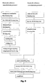
- FIG. 4 is similar to Fig. 3 which is the process flow chart of Example 1, except that a step of irradiating the protective film with vacuum UV rays is further included and diethylene glycol monobutyl ether acetate is used as the driving voltage-reducing compound.
- vacuum UV rays As the vacuum UV rays, Xe molecule rays of 172 nm with an energy of 10 mW/cm 2 are emitted for 5 minutes (vacuum UV ray irradiation step). This irradiation allows CO 2 to be removed from MgCO 3 formed on the surface of MgO, so that it is possible to improve the activity on the MgO surface.
- the driving voltage for the PDP thus obtained can be reduced by about 10 V compared to the PDP in which the protective film is not treated with diethylene glycol monobutyl ether acetate.
- FIG. 5 is similar to Fig. 3 which is the process flow chart of Example 1, except that a step of heating the protective film and a step of cooling the same to room temperature are further included, methane gas is used as the driving voltage-reducing compound, and the protective film is exposed to an atmosphere of methane gas in an airtight state (driving voltage-reducing compound treatment step).
- Heating of the protective film was continued at 300°C for 30 minutes (heating step), and cooling of the protective film was conducted by lowering the temperature to room temperature (about 25°C) by letting it stand for 60 minutes (cooling step). Since CO 2 can be removed from MgCO 3 formed on the surface of MgO by the heating step, it is possible to improve the activity on the MgO surface.
- the driving voltage for the PDP thus obtained can be reduced by about 10 V compared to the PDP in which the protective film is not treated with methane.
- the embodiments of the present invention it is possible to reduce the driving voltage compared to the conventional gas discharge panel having a protective film not containing the driving voltage-reducing compound. Accordingly, it is possible to provide a gas discharge panel of low power consumption and lower generation of electromagnetic radiation. Moreover, since the necessity of using an expensive, high pressure resistant driving circuit device is eliminated, it is possible to provide a low-priced display device.
Applications Claiming Priority (2)
| Application Number | Priority Date | Filing Date | Title |
|---|---|---|---|
| JP2002318120 | 2002-10-31 | ||
| JP2002318120A JP4056357B2 (ja) | 2002-10-31 | 2002-10-31 | ガス放電パネル及びその製造方法 |
Publications (2)
| Publication Number | Publication Date |
|---|---|
| EP1416510A2 true EP1416510A2 (fr) | 2004-05-06 |
| EP1416510A3 EP1416510A3 (fr) | 2006-05-10 |
Family
ID=32089585
Family Applications (1)
| Application Number | Title | Priority Date | Filing Date |
|---|---|---|---|
| EP03256366A Withdrawn EP1416510A3 (fr) | 2002-10-31 | 2003-10-09 | Panneau à décharge gazeuse et procédé de production de celui-ci |
Country Status (5)
| Country | Link |
|---|---|
| US (2) | US6984937B2 (fr) |
| EP (1) | EP1416510A3 (fr) |
| JP (1) | JP4056357B2 (fr) |
| KR (2) | KR20040038633A (fr) |
| TW (1) | TWI292919B (fr) |
Cited By (1)
| Publication number | Priority date | Publication date | Assignee | Title |
|---|---|---|---|---|
| EP2184758A1 (fr) * | 2008-06-26 | 2010-05-12 | Panasonic Corporation | Procédé de production d'un panneau d'affichage plasma |
Families Citing this family (5)
| Publication number | Priority date | Publication date | Assignee | Title |
|---|---|---|---|---|
| US20070262715A1 (en) * | 2006-05-11 | 2007-11-15 | Matsushita Electric Industrial Co., Ltd. | Plasma display panel with low voltage material |
| RU2441297C2 (ru) * | 2007-06-15 | 2012-01-27 | Улвак, Инк. | Способ и устройство для производства плазменной отображающей панели |
| JP4589980B2 (ja) * | 2008-06-04 | 2010-12-01 | パナソニック株式会社 | プラズマディスプレイパネルの製造方法 |
| CN102365702A (zh) * | 2010-02-12 | 2012-02-29 | 松下电器产业株式会社 | 等离子显示面板 |
| US8742194B2 (en) * | 2012-05-21 | 2014-06-03 | CM Global Systems, LLC | Hydrocarbon-containing mixture and method and system for making the same |
Citations (4)
| Publication number | Priority date | Publication date | Assignee | Title |
|---|---|---|---|---|
| JPH08255562A (ja) * | 1995-03-17 | 1996-10-01 | Fujitsu Ltd | Pdpにおける誘電体用保護膜の形成方法 |
| JP2001035382A (ja) * | 1998-06-30 | 2001-02-09 | Mitsubishi Materials Corp | Fpd用保護膜及びその製造方法並びにこれを用いたfpd |
| EP1164620A2 (fr) * | 1995-12-15 | 2001-12-19 | Matsushita Electric Industrial Co., Ltd. | Panneau d'affichage à plasma convenant à l'affichage de haute qualité et procédé de fabrication |
| US6437506B1 (en) * | 1995-10-09 | 2002-08-20 | Dai Nippon Printing Co., Ltd. | Sol solution and method for film formation |
Family Cites Families (7)
| Publication number | Priority date | Publication date | Assignee | Title |
|---|---|---|---|---|
| JP2984014B2 (ja) | 1990-02-01 | 1999-11-29 | 富士通株式会社 | プラズマディスプレイパネルの製造方法 |
| JPH0992161A (ja) | 1995-09-20 | 1997-04-04 | Fujitsu Ltd | プラズマ・ディスプレイ・パネル |
| KR100899311B1 (ko) * | 1998-12-10 | 2009-05-27 | 미쓰비시 마테리알 가부시키가이샤 | Fpd 용 보호막 및 그 제조방법 그리고 이것을 사용한 fpd |
| KR100798986B1 (ko) * | 2000-03-31 | 2008-01-28 | 마츠시타 덴끼 산교 가부시키가이샤 | 플라즈마 디스플레이 패널의 제조방법 |
| JP4153983B2 (ja) * | 2000-07-17 | 2008-09-24 | パイオニア株式会社 | 保護膜、その成膜方法、プラズマディスプレイパネル及びその製造方法 |
| JP4566465B2 (ja) * | 2001-06-21 | 2010-10-20 | パナソニック株式会社 | プラズマディスプレイパネル |
| JP4698077B2 (ja) * | 2001-07-18 | 2011-06-08 | パナソニック株式会社 | プラズマディスプレイパネルおよびその製造方法 |
-
2002
- 2002-10-31 JP JP2002318120A patent/JP4056357B2/ja not_active Expired - Fee Related
-
2003
- 2003-09-03 US US10/653,228 patent/US6984937B2/en not_active Expired - Fee Related
- 2003-09-09 KR KR1020030062976A patent/KR20040038633A/ko not_active Application Discontinuation
- 2003-09-22 TW TW092126094A patent/TWI292919B/zh active
- 2003-10-09 EP EP03256366A patent/EP1416510A3/fr not_active Withdrawn
-
2005
- 2005-10-25 US US11/257,109 patent/US7458871B2/en not_active Expired - Fee Related
-
2008
- 2008-09-24 KR KR1020080093672A patent/KR20080092321A/ko not_active Application Discontinuation
Patent Citations (4)
| Publication number | Priority date | Publication date | Assignee | Title |
|---|---|---|---|---|
| JPH08255562A (ja) * | 1995-03-17 | 1996-10-01 | Fujitsu Ltd | Pdpにおける誘電体用保護膜の形成方法 |
| US6437506B1 (en) * | 1995-10-09 | 2002-08-20 | Dai Nippon Printing Co., Ltd. | Sol solution and method for film formation |
| EP1164620A2 (fr) * | 1995-12-15 | 2001-12-19 | Matsushita Electric Industrial Co., Ltd. | Panneau d'affichage à plasma convenant à l'affichage de haute qualité et procédé de fabrication |
| JP2001035382A (ja) * | 1998-06-30 | 2001-02-09 | Mitsubishi Materials Corp | Fpd用保護膜及びその製造方法並びにこれを用いたfpd |
Non-Patent Citations (3)
| Title |
|---|
| DATABASE COMPENDEX [Online] ENGINEERING INFORMATION, INC., NEW YORK, NY, US; LEE W T ET AL: "Studies on a LaF3-coated MgO protecting layer in AC-plasma-display panels" XP002370964 Database accession no. E2001296580924 & J SOC INF DISP; JOURNAL OF THE SOCIETY FOR INFORMATION DISPLAY 2001, vol. 9, no. 1, 15 February 1999 (1999-02-15), pages 35-40, * |
| PATENT ABSTRACTS OF JAPAN vol. 1997, no. 02, 28 February 1997 (1997-02-28) & JP 08 255562 A (FUJITSU LTD), 1 October 1996 (1996-10-01) * |
| PATENT ABSTRACTS OF JAPAN vol. 2000, no. 19, 5 June 2001 (2001-06-05) & JP 2001 035382 A (MITSUBISHI MATERIALS CORP), 9 February 2001 (2001-02-09) -& US 6 821 616 B1 23 November 2004 (2004-11-23) * |
Cited By (2)
| Publication number | Priority date | Publication date | Assignee | Title |
|---|---|---|---|---|
| EP2184758A1 (fr) * | 2008-06-26 | 2010-05-12 | Panasonic Corporation | Procédé de production d'un panneau d'affichage plasma |
| EP2184758A4 (fr) * | 2008-06-26 | 2011-08-03 | Panasonic Corp | Procédé de production d'un panneau d'affichage plasma |
Also Published As
| Publication number | Publication date |
|---|---|
| TWI292919B (en) | 2008-01-21 |
| US6984937B2 (en) | 2006-01-10 |
| TW200411697A (en) | 2004-07-01 |
| US20040085022A1 (en) | 2004-05-06 |
| US20060043897A1 (en) | 2006-03-02 |
| KR20040038633A (ko) | 2004-05-08 |
| US7458871B2 (en) | 2008-12-02 |
| JP2004152673A (ja) | 2004-05-27 |
| JP4056357B2 (ja) | 2008-03-05 |
| KR20080092321A (ko) | 2008-10-15 |
| EP1416510A3 (fr) | 2006-05-10 |
Similar Documents
| Publication | Publication Date | Title |
|---|---|---|
| JP4505474B2 (ja) | プラズマディスプレイパネル | |
| WO2005098889A1 (fr) | Écran d’affichage à décharge gazeuse | |
| WO2005109464A1 (fr) | Panneau d’affichage à plasma | |
| JP3623406B2 (ja) | ガス放電パネルとその製造方法 | |
| US7458871B2 (en) | Gas discharge panel production method | |
| JP4543852B2 (ja) | プラズマディスプレイパネル | |
| WO2011142138A1 (fr) | Panneau d'affichage plasma et son procédé de production | |
| JP2003022755A (ja) | プラズマディスプレイパネル用基板、その製造方法、その保護膜成膜装置、およびプラズマディスプレイパネル | |
| KR100719580B1 (ko) | 평판 디스플레이 장치 | |
| CN100583360C (zh) | 气体放电显示面板 | |
| WO2011138870A1 (fr) | Panneau d'affichage à plasma | |
| WO2010095344A1 (fr) | Ecran plasma | |
| JP2009301841A (ja) | プラズマディスプレイパネル | |
| JP2004146231A (ja) | プラズマディスプレイパネルの製造方法 | |
| JP2004327114A (ja) | ガス放電パネル | |
| JP2001135241A (ja) | ガス放電パネル及びその製造方法 | |
| JP4835318B2 (ja) | プラズマディスプレイパネルおよびその製造方法 | |
| JP2013008583A (ja) | プラズマディスプレイパネルの保護層及びプラズマディスプレイパネル | |
| JP2005123174A (ja) | プラズマディスプレイパネルとその製造方法およびその保護層用材料 | |
| JP2003346663A (ja) | プラズマディスプレイパネル | |
| JP2013008507A (ja) | プラズマディスプレイパネル | |
| JP2004265658A (ja) | プラズマディスプレイパネル | |
| JP2004265656A (ja) | プラズマディスプレイパネルおよびその製造方法 | |
| JP2009187942A (ja) | プラズマディスプレイパネルとその製造方法 | |
| JP2013008508A (ja) | プラズマディスプレイパネル |
Legal Events
| Date | Code | Title | Description |
|---|---|---|---|
| PUAI | Public reference made under article 153(3) epc to a published international application that has entered the european phase |
Free format text: ORIGINAL CODE: 0009012 |
|
| AK | Designated contracting states |
Kind code of ref document: A2 Designated state(s): AT BE BG CH CY CZ DE DK EE ES FI FR GB GR HU IE IT LI LU MC NL PT RO SE SI SK TR |
|
| AX | Request for extension of the european patent |
Extension state: AL LT LV MK |
|
| PUAL | Search report despatched |
Free format text: ORIGINAL CODE: 0009013 |
|
| AK | Designated contracting states |
Kind code of ref document: A3 Designated state(s): AT BE BG CH CY CZ DE DK EE ES FI FR GB GR HU IE IT LI LU MC NL PT RO SE SI SK TR |
|
| AX | Request for extension of the european patent |
Extension state: AL LT LV MK |
|
| 17P | Request for examination filed |
Effective date: 20061106 |
|
| AKX | Designation fees paid |
Designated state(s): DE FR GB |
|
| 17Q | First examination report despatched |
Effective date: 20070912 |
|
| RAP1 | Party data changed (applicant data changed or rights of an application transferred) |
Owner name: HITACHI PLASMA DISPLAY LIMITED |
|
| GRAP | Despatch of communication of intention to grant a patent |
Free format text: ORIGINAL CODE: EPIDOSNIGR1 |
|
| STAA | Information on the status of an ep patent application or granted ep patent |
Free format text: STATUS: THE APPLICATION IS DEEMED TO BE WITHDRAWN |
|
| 18D | Application deemed to be withdrawn |
Effective date: 20091230 |