EP1401134B1 - Automatic gain control circuit and method and demodulation apparatus - Google Patents
Automatic gain control circuit and method and demodulation apparatus Download PDFInfo
- Publication number
- EP1401134B1 EP1401134B1 EP02741298A EP02741298A EP1401134B1 EP 1401134 B1 EP1401134 B1 EP 1401134B1 EP 02741298 A EP02741298 A EP 02741298A EP 02741298 A EP02741298 A EP 02741298A EP 1401134 B1 EP1401134 B1 EP 1401134B1
- Authority
- EP
- European Patent Office
- Prior art keywords
- gain
- signal
- reception signal
- burst
- gain control
- Prior art date
- Legal status (The legal status is an assumption and is not a legal conclusion. Google has not performed a legal analysis and makes no representation as to the accuracy of the status listed.)
- Expired - Fee Related
Links
- 238000000034 method Methods 0.000 title claims description 30
- 238000001514 detection method Methods 0.000 claims description 147
- 230000003321 amplification Effects 0.000 claims description 112
- 238000003199 nucleic acid amplification method Methods 0.000 claims description 112
- 238000012545 processing Methods 0.000 description 38
- 238000004891 communication Methods 0.000 description 25
- 238000010586 diagram Methods 0.000 description 15
- 230000001934 delay Effects 0.000 description 11
- 230000003111 delayed effect Effects 0.000 description 8
- 238000005070 sampling Methods 0.000 description 7
- 230000006866 deterioration Effects 0.000 description 6
- 230000005540 biological transmission Effects 0.000 description 5
- 238000006243 chemical reaction Methods 0.000 description 5
- 238000012546 transfer Methods 0.000 description 5
- 238000012937 correction Methods 0.000 description 3
- 230000010355 oscillation Effects 0.000 description 3
- 230000001960 triggered effect Effects 0.000 description 3
- 101150097504 LHX1 gene Proteins 0.000 description 2
- 239000000969 carrier Substances 0.000 description 2
- 101000710013 Homo sapiens Reversion-inducing cysteine-rich protein with Kazal motifs Proteins 0.000 description 1
- 230000002542 deteriorative effect Effects 0.000 description 1
- 230000000694 effects Effects 0.000 description 1
- 238000012544 monitoring process Methods 0.000 description 1
- 230000002035 prolonged effect Effects 0.000 description 1
- 238000011084 recovery Methods 0.000 description 1
- 230000000630 rising effect Effects 0.000 description 1
- 230000001360 synchronised effect Effects 0.000 description 1
Images


Classifications
-
- H—ELECTRICITY
- H03—ELECTRONIC CIRCUITRY
- H03G—CONTROL OF AMPLIFICATION
- H03G3/00—Gain control in amplifiers or frequency changers
- H03G3/20—Automatic control
- H03G3/30—Automatic control in amplifiers having semiconductor devices
- H03G3/3052—Automatic control in amplifiers having semiconductor devices in bandpass amplifiers (H.F. or I.F.) or in frequency-changers used in a (super)heterodyne receiver
- H03G3/3078—Circuits generating control signals for digitally modulated signals
-
- H—ELECTRICITY
- H03—ELECTRONIC CIRCUITRY
- H03G—CONTROL OF AMPLIFICATION
- H03G3/00—Gain control in amplifiers or frequency changers
- H03G3/20—Automatic control
- H03G3/30—Automatic control in amplifiers having semiconductor devices
- H03G3/3052—Automatic control in amplifiers having semiconductor devices in bandpass amplifiers (H.F. or I.F.) or in frequency-changers used in a (super)heterodyne receiver
-
- H—ELECTRICITY
- H04—ELECTRIC COMMUNICATION TECHNIQUE
- H04L—TRANSMISSION OF DIGITAL INFORMATION, e.g. TELEGRAPHIC COMMUNICATION
- H04L27/00—Modulated-carrier systems
- H04L27/26—Systems using multi-frequency codes
- H04L27/2601—Multicarrier modulation systems
- H04L27/2647—Arrangements specific to the receiver only
Definitions
- the present invention relates to an automatic gain control circuit that may, for example, be applied to a receiver etc. of a wireless communication system, an automatic gain control method, and a demodulation apparatus using the circuit.
- a particularly preferred form of implementation of the invention relates to an automatic gain control circuit and method, and a demodulation apparatus using the same, applied to for example a wireless communication system for receiving a radio signal which is modulated by an orthogonal frequency division multiplexing (OFDM) modulation method and includes a burst signal including a preamble signal at the header of this modulated packet signal.
- OFDM orthogonal frequency division multiplexing
- A/D analog-to-digital
- the reception signal levels will differ largely according to transmission outputs of the individual apparatuses and the distance between apparatuses.
- a synchronization demodulation apparatus of a wireless communication system mounts an automatic gain control (AGC) circuit as a circuit for adjusting the reception signal level to within the dynamic range of the A/D converter.
- AGC automatic gain control
- a burst signal referred to as a preamble signal is transmitted inserted at the header of the modulated signal.
- the AGC circuit mounted in the synchronization demodulation apparatus synchronizes the timing to within the period of this burst signal, while controls the amplification gain based on the received level of the burst signal.
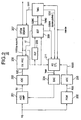
- FIG. 1 is a block diagram of an example of the configuration of a demodulation apparatus mounting a conventional AGC circuit able to be applied to a wireless communication system using burst synchronization.
- FIG. 1 The apparatus of FIG. 1 is disclosed in Japanese Unexamined Patent Publication (Kokai) No. 11-205278 .
- This demodulation apparatus 10 is comprised of an automatic gain control amplifier (AGCAMP) 101, A/D converter (ADC) 102, OFDM demodulator (DEMOD) 103, delay unit (DLY) 104, burst detector (BDT) 105, packet detector (PDT) 106, and amplification gain controller (AGCTL) 107.
- AGCAMP automatic gain control amplifier
- ADC A/D converter
- DEMOD OFDM demodulator
- DLY delay unit
- BDT burst detector
- PDT packet detector
- ACTL amplification gain controller
- an OFDM reception signal RS received by a not illustrated antenna is input to the automatic gain control amplifier 101.
- the reception signal RS is automatically controlled in gain and output as the optimum signal level to the A/D converter 102.
- the automatic gain control amplifier 101 controls the case of automatic gain control by a control signal S107 by the amplification gain controller 107 and the case where the control gain is fixed.
- the A/D converter 102 converts the input reception signal from an analog signal to digital signal and outputs a digital reception signal S102 to the OFDM demodulator 103, delay unit 104, and burst detector 105.
- the OFDM demodulator 103 applies a discrete Fourier transform to the digital reception signal S102 based on the output of the burst detector 105 to demodulate the OFDM signal and outputs this demodulated signal S103 to the packet detector 106 and following processing circuit.
- the delay unit 104 delays the digital reception signal S102 by the amount of the burst period and outputs the result as the signal S104 to the burst detector 105.
- the burst detector 105 establishes correlation between the digital reception signal S102 and the delay signal S104, detects the burst signal of the period determined by the communication system, and outputs the detected result as the signal S105 to the OFDM demodulator 103 and the amplification gain controller 107.
- the packet detector 106 detects a unique word of the packet header from the demodulation signal S103 by the OFDM demodulator 103, detects whether or not the packets were correctly demodulated, detects the end time of the packets, and outputs the detected result as the signal S106 to the amplification gain controller 107.
- the amplification gain controller 107 judges whether or not to fix the automatic gain control of the automatic gain control amplifier 101 based on the output signal S105 by the burst detector 105 and the output signal S106 of the packet detector 106 and outputs the judged result as the control signal S107 to the automatic gain control amplifier 101.
- the demodulation apparatus of FIG. 1 fixes or changes the control gain in the automatic gain control amplifier 101 according to whether or not the burst synchronization was established in the burst synchronization system, so it is suitable for a burst synchronization communication system for communication dividing the timing of the burst synchronization and the timing of the data and/or packets.
- the OFDM modulation method is a modulation method applies an inverse Fourier transform to 2 n primary modulated (QPSK, 16ASAM, etc.) transmitted signal symbols to form 2 n number of sub carriers orthogonal to each other on the frequency axis.
- the OFDM modulation signal of the OFDM modulation method is a combined signal of a plurality of modulation waves, so the ratio of the peak amplitude to the mean amplitude is large and the fluctuation in amplitude is large.
- the reception signal levels differ largely according to the transmitted outputs of the individual apparatuses and the distance between apparatuses. Therefore, in an automatic gain control circuit having a long time constant, the optimum gain is not pulled into for the individual packets, but the mean gain of the optimum gains of all packets is pulled into and therefore there is the possibility that the system will end up crashing.
- the present invention was made in the light of such circumstances and has as an object thereof to provide an automatic gain control circuit and method and a demodulation apparatus using the same able to realize high speed, accurate level acquisition and in turn able to prevent occurrence of error and able to prevent crashing of the system.
- the present invention provides an AGC circuit as set forth in claim 1 hereof, a demodulation apparatus as set forth in claim 35 hereof, and an ACG method as set forth in claim 37 hereof.
- the gain control signal is output to the automatic gain control amplifier from the amplification gain controller, and the amplification gain of the automatic gain control amplifier is set at a value set in advance, for example, the first gain of the maximum value.
- the preamble signal at the header of the reception signal is input to the automatic gain control amplifier.
- the automatic gain control amplifier for example, amplifies a front half section of the preamble signal of the reception signal with the first gain (maximum gain) and outputs the result to for example an A/D converter.
- the preamble signal of the reception signal is input to the reception signal power monitor.
- the reception signal power monitor monitors the power of the reception signal, measures for example the peak voltage, and supplies a reception signal power value taking a value in accordance with the input reception signal level to the amplification gain controller.
- the A/D converter converts the preamble signal portion of the reception signal from an analog signal to a digital signal and supplies it to the amplification gain controller, delay unit, and burst detector.
- the output signal of the A/D converter ends up being distorted, but since it is not a data signal, deterioration of the quality of the reception signal is not caused.
- the delay unit delays the digital reception signal by the amount of the burst period for burst detection and outputs the result to the burst detector.
- the burst detector performs a correlation (auto-correlation and cross-correlation) operation between the digital reception signal from the A/D converter and the delay signal from the delay unit.
- the auto-correlation result detects a burst signal of a period determined by the communication system, first generates a first synchronization detection signal indicating that the front half X section of the preamble signal is detected, and outputs the same to the amplification gain controller.
- burst detection is possible without lowering the detection rate.
- the amplification gain controller receives the first burst synchronization detection signal from the burst detector, calculates the gain based on the reception signal power value detected at the reception signal monitor and a suitable value not distorting the A/D converter, and sets the gain control signal at the calculated value.
- This gain control signal is supplied to the automatic gain control amplifier.
- the automatic gain control amplifier receives the gain control signal and sets the gain at the second gain as the calculated value.
- the gain of the automatic gain control amplifier includes analog signal processing in the step of calculation of the peak value of the reception signal power, includes slight variation, and is therefore rough gain control.
- the automatic gain control amplifier amplifies for example the remaining front half section and rear half section of the preamble signal of the reception signal with the gain in accordance with the reception signal level and outputs the result to the A/D converter.
- the A/D converter converts the preamble signal portion of the reception signal from an analog signal to a digital signal and supplies it to the amplification gain controller, delay unit, and burst detector.
- the input signal of the A/D converter is amplified with a gain based on a suitable value not distorting the A/D converter, so distortion does not occur in the output signal of the A/D converter.
- the delay unit delays the digital reception signal by the amount of the burst period for the burst detection and outputs the result to the burst detector.
- the burst detector performs the correlation (auto-correlation and cross-correlation) operation between the digital reception signal from the A/D converter and the delay signal from the delay unit.
- the auto-correlation result detects the burst signal of the period determined by the communication system, generates a second synchronization detection signal indicating that the front half X section of the preamble signal is detected, and outputs it to the amplification gain controller.
- the amplification gain controller receives the signal passed through the A/D converter without distortion by a gain based on the reception signal power, integrates for example the digital value of the reception signal, and measures the correct signal power value.
- the amplification gain controller receives the second burst synchronization detection signal from the burst detector, calculates the gain based on the digital integrated value of the reception signal passed through the A/D converter without distortion and the optimum value not distorting the A/D converter, and sets the gain control signal at the calculated value.
- This gain control signal is supplied to the automatic gain control amplifier.
- the automatic gain control amplifier receives the gain control signal and sets the gain at the third gain as the optimum calculated value.
- the automatic gain control amplifier amplifies the Y section of the remaining rear half of the preamble signal and the reference signal and data signal of the reception signal with a gain in accordance with the reception signal level and outputs the result to the A/D converter.
- the A/D converter converts the reference signal and data portion of the reception signal from an analog signal to a digital signal and supplies them to the amplification gain controller, delay unit, and burst detector.
- the delay unit delays the digital reception signal by the amount of the burst period for the burst detection and output the result to the burst detector.
- the burst detector performs the correlation (auto-correlation and cross-correlation) operation between the digital reception signal from the A/D converter and the delay signal from the delay unit.
- the timing controller supplies the cross-correlation power of the cross-correlation result to the timing controller, monitors the peak timing based on the power, and outputs the third synchronization detection signal to the amplification gain controller after a predetermined time from this peak timing.
- the amplification gain controller receiving the third synchronization detection signal returns to the initial mode, that is, the waiting mode of the trigger signal.
- FIG. 1 is a block diagram of an example of the configuration of a demodulation apparatus mounting a conventional AGC circuit able to be applied to a wireless communication system using a burst synchronization.
- FIG. 2 is a block diagram of the configuration of an embodiment of a burst synchronization demodulation apparatus to which an automatic gain control circuit according to the present invention is applied.
- FIG. 3 is a view showing a burst signal portion including a representative preamble signal of an IEEE 802.11a system.
- FIG. 4 is a view showing a burst signal portion including a representative preamble signal of a BRAN system.
- FIG. 5 is a view showing a burst signal portion including a representative preamble signal of a Wireless 1394 system.
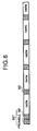
- FIG. 6 is a view showing a signal format wherein a reference signal REF is inserted in a data signal section of a constant period or more in the Wireless 1394 system.
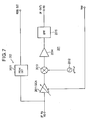
- FIG. 7 is a circuit diagram showing a concrete configuration of an automatic gain control amplifier of FIG. 2.
- FIG. 8 is a view showing an example of a gain control characteristic of the gain control amplifier of FIG. 7.
- FIG. 9 is a view showing an output characteristic of a reception signal power monitor for the input level of the reception signal.
- FIG. 10 is a circuit diagram showing a concrete example of the configuration of a reception signal processing unit of FIG. 2.
- FIG. 11 is a circuit diagram showing a concrete example of the configuration of a burst detector and a timing controller of FIG. 2.
- FIG. 12 is a circuit diagram showing an example of the configuration of an auto-correlation circuit of FIG. 11.
- FIG. 13 is a circuit diagram showing the example of the configuration of a cross-correlation circuit of FIG. 11.
- FIGS. 14A to 14G are views showing timing charts from the auto-correlation processing of the burst detector to when synchronization detection signals xpulse and ypulse are output.
- FIGS. 15A to 15F are views showing timing charts from the cross-correlation processing of the burst detector to when a synchronization detection signal cpulse and an FFT timing signal TFFT are output.
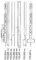
- FIG. 16 is a flow chart for explaining a first stage of a gain control operation in the amplification gain controller according to the present invention.
- FIG. 17 is a flow chart for explaining a second stage of a gain control operation in the amplification gain controller according to the present invention.
- FIG. 18 is a flow chart for explaining a third stage of a gain control operation in the amplification gain controller according to the present invention.
- FIG. 19 is a circuit diagram showing a concrete example of the configuration of the amplification gain controller of FIG. 2.
- FIGS. 20A to 20H are views showing timing charts for explaining the operation of the amplification gain controller of FIG. 19.
- FIG. 2 is a block diagram of the configuration of an embodiment of a burst synchronization demodulation apparatus to which an automatic gain control circuit according to the present invention is applied.
- the burst synchronization demodulation apparatus 20 has, as shown in FIG. 2, an automatic gain control amplifier (AGCAMP) 201, reception signal power monitor (POW) 202, A/D converter (ADC) 203, digital-to-analog (D/A) converter (DAC) 204, A/D converter (ADC) 205, reception signal processing unit (RXPRC) 206, OFDM demodulator (DEMOD) 207, delay unit (DLY) 208, burst detector (BDT) 209, timing controller (TMG) 210, and amplification gain controller (AGCTL) 211 as main components.
- AGCAMP automatic gain control amplifier
- burst synchronization communication system As an example of the burst synchronization communication system, an explanation will be given of the automatic gain control system of a burst synchronization demodulation apparatus of a 5 GHz band wireless LAN system.
- the 5 GHz band wireless LAN system employs the OFDM modulation method for realizing excellent communication performance over a broad band.
- the OFDM modulation method is large in strength against ghosts and multi-paths, but in contrast is weak in strength against nonlinearity of the circuit.
- a burst signal of 10 to 20 microseconds referred to as a "preamble signal" into the header of the modulation signal, take the timing synchronization in this section, on the one hand to perform level acquisition of the voltage amplitude of the signal input to the A/D converter 203 within a signal tolerance range where distortion does not occur.
- the several microseconds of the rear half of the preamble signal include a reference signal for monitoring the frequency characteristic of a channel and correcting a data signal following the preamble signal (actual communication data).
- a reference signal for monitoring the frequency characteristic of a channel and correcting a data signal following the preamble signal (actual communication data).
- fluctuation of the level of the digital signal output from the A/D converter 203 is not permitted. It is necessary to hold the gain of the automatic gain control amplifier 201 constant.
- FIG. 3 is a view showing a burst signal portion including the representative preamble signal of the IEEE 802.11a system
- FIG. 4 is a view showing a burst signal portion including a representative preamble signal of the BRAN system
- FIG. 5 is a view showing a burst signal portion including a representative preamble signal of the Wireless 1394 system.
- A16, B16, etc. represent the pattern identification and the burst period, while IA16 represents the pattern of the A16 phase inverted.
- C64 represents the reference signal, while C16 and C32 indicate guard interval portions.
- the pattern B16 is repeated 10 times.
- the first 5 periods are different (A16, IA16, A16, IA16, IA16).
- all of the 10 periods are different patterns. Concretely, they become patterns of A16, IA16, A16, IA16, A16, A16, IA16, A16, IA16, IA16, IA16.
- a synchronous transfer mode is supported, so a continuous signal such as a video signal can be communicated.
- the transmission characteristic changes from the transmission characteristic at the time of the reception of the reference signal in the preamble signal at the header of the reception signal under the multi-path environment, and the reception performance ends up deteriorating.
- the data signal section of the constant period or more, as shown in FIG. 6, has a reference signal REF inserted in it. Due to this, the transmission characteristic is measured again for every reference signal, and deterioration of the reception performance is prevented.
- the components of the demodulation apparatus for demodulating the reception signal when a burst signal portion including a signal of 10 to 20 microseconds referred to as a "preamble signal" is inserted in the header of the modulation signal as described above have the following configurations and functions.
- the automatic gain control amplifier 201 automatically controls the gain of the reception signal RS received at a not illustrated antenna based on the level of a gain control signal Vagc from the amplification gain controller 211 supplied via the DAC 204 and outputs the signal RX of the intended level to the A/D converter 203. Note that, the automatic gain control amplifier 201 is controlled between the case of automatic gain control by the gain control signal Vagc from the amplification gain controller 211 and the case of fixing the control gain.
- FIG. 7 is a circuit diagram showing a concrete configuration of the automatic gain control amplifier 201.
- the automatic gain control amplifier 201 has, as shown in FIG. 7, a gain control amplifier (GCA) 2011, local oscillator 2012, multiplier 2013, amplifier 2014, and band pass filter (BPF) 2015 having a band width of several tens MHz.
- GCA gain control amplifier
- BPF band pass filter
- a frequency conversion circuit is configured by the local oscillator 2012 and the multiplier 2013 among these components.
- the local oscillator 2012 outputs for example a signal e[j2nf cw t] of the carrier frequency f cw to the multiplier 2013. Note, the [ ] indicates the power of e.
- the gain control amplifier 2011 amplifies the reception signal (IF input signal) RS with the gain determined by the gain control signal Vagc, the amplified signal is converted in frequency by the frequency conversion circuit comprised of the local oscillator 2012 and the multiplier 2013, and then the BPF 2015 restricts the band to obtain the output signal (IF output) RX.
- FIG. 8 is a view showing the gain control characteristic of the gain control amplifier 2011 of FIG. 7.
- the abscissa indicates the gain control signal Vagc, and the ordinate indicates the gain.
- the gain control amplifier 2011 linearly changes the gain from 0 to 80 dB within a range where the gain control signal Vagc is 0V to 1V.
- control gain range is 80 dB.
- the reception signal power monitor 202 includes a peak detection circuit (Peak Det) 2021 as the peak value detection circuit as shown in FIG. 7, measures the peak voltage of the reception signal RS, converts it to a field strength signal RSSI of a voltage signal taking a value in accordance with the input reception signal level, and outputs the same to the A/D converter 205.
- Peak Det Peak Det
- the monitor detects not the mean value, but the peak value. Note that, it gives a reset signal at the time of start of the burst detection, resets the peak detection circuit (Peak Det) 2021, and monitors the maximum peak value after that.
- FIG. 9 is a view showing the output characteristic of the reception signal power monitor 202 for the input level of the reception signal.
- the abscissa indicates the input level, and the ordinate indicates the voltage of the field strength signal RRSI.
- the voltage of the field strength signal RSSI linearly changes from 0V to 2V within the range where the input level is -70 dBv to -20 dBv.
- the A/D converter 203 converts the analog reception signal RX output from the automatic gain control amplifier 201 to a digital signal and outputs the same as the digital reception signal RXD to the reception signal processing unit 206.
- the D/A converter 204 converts the gain control signal Vagc generated at the amplification gain controller 211 from a digital signal to an analog signal and outputs the same to the automatic gain control amplifier 201.
- the A/D converter 205 converts the field strength signal RSSI output from the reception signal power monitor 202 from the analog signal to a digital signal and outputs it to the amplification gain controller 211.
- the reception signal processing unit 206 converts the digital reception signal RXD to baseband signals bb_re (real portion) and bb_im (imaginary portion), converts the sampling frequency of the baseband signal to a low frequency (performs down sampling), performs complex multiplication based on an error detection frequency ⁇ f by the burst detector 209 to correct the frequency offset, generates the signal S206 (sy_re and sy_im), and outputs the same to the OFDM demodulator 207, delay unit 208, burst detector 209, and amplification gain controller 211.
- FIG. 10 is a circuit diagram showing a concrete example of the configuration of the reception signal processing unit 206 of FIG. 2.
- the present reception signal processing unit 206 is configured by, as shown in FIG. 10, a baseband conversion circuit 2061, digital low pass filters (LPF) 2062 and 2063, down convert circuits 2064 and 2065, and a frequency offset correction circuit 2066.
- a baseband conversion circuit 2061 digital low pass filters (LPF) 2062 and 2063
- LPF digital low pass filters
- the baseband conversion circuit 2061 is configured by a local oscillator 20611 and multipliers 20612 and 20613.
- the baseband conversion circuit 2061 multiplies the reception signal RXD (if) by the carrier frequency f cw at the multipliers 20612 and 20613 to convert the input reception signal RXD (if) to the baseband signals bb_re and bb_im as shown in Equation (1) and supplies the results to the LPF 2062 and 2063.
- the LPF 2062 and 2063 have for example linear phase FIR (finite impulse response) transversal type circuit configurations.
- the LPF 2062 is configured by (n-1) number of delay units 1re-1 to 1re-n-1 cascade connected with the input line of the baseband signal bb_re and configuring a shift register, n number of multipliers 2re-1 to 2re-n for multiplying the input baseband signal bb_re and the output signals of the delay units 1re-1 to lre-n-1 with filter coefficients h(0) to h(n-1), and an adder 3re for adding the output signals of the n number of multipliers 2re-1 to 2re-n and outputting the result to the down convert circuit 2064.
- the LPF 2063 is configured by (n-1) number of delay units lim-1 to lim-n-1 cascade connected with the input line of the baseband signal bb_im and configuring a shift register, n number of multipliers 2im-1 to 2im-n for multiplying the input baseband signal bb_im and the output signals of the delay units lim-1 to lim-n-1 with the filter coefficients h(0) to h(n-1), and an adder 3im for adding the output signals of the n number multipliers 2im-1 to 2im-n and outputting the result to the down convert circuit 2064.
- LPFs 2062 and 2063 and down convert circuits 2064 and 2065 convert the sampling frequencies of the baseband signals bb_re and bb_im to a signal dc_re of for example 100 MHz to 25 MHz.
- the LPFs 2062 and 2063 restrict the bands of the baseband signals bb_re and bb_im and prevents adjacent carriers from being aliased.
- timing of the down sampling at the down convert circuits 2064 and 2065 thins out the clock upon receipt of the supply of a signal En.
- the frequency offset correction circuit 2066 is configured by a local oscillator 20661, multipliers 20662 to 20665, and adders 20666 and 20667.
- the frequency offset correction circuit 2066 reflects the error detection frequency ⁇ f given from the burst detector 209 in the oscillation output of the local oscillator 20661, complex multiplies this oscillation output and the signal dc_re at the multipliers 20662 and 20665, complex multiplies the oscillation output and the signal dc_im at the multipliers 20663 and 20664, adds the outputs of the multiplier 20662 and the multiplier 20663 at the adder 20666, and adds the outputs of the multiplier 20664 and the multiplier 20665 at the adder 20667 thereby to generate the signals sy_re and sy_im as shown in the following Equations (2) and (3) and outputs the same to the OFDM demodulator 207, delay unit 208, burst detector 209, and amplification gain controller 211.
- sy_re dc_re ⁇ cos ( 2 ⁇ ⁇ f cw ⁇ t ) + dc_im x sin 2 ⁇ ⁇ f cw ⁇ t
- sy_im dc_im ⁇ cos ( 2 ⁇ ⁇ f cw ⁇ t ) - dc_re x sin 2 ⁇ ⁇ f cw ⁇ t
- the OFDM demodulator 207 processes the output signal S206 of the reception signal processing unit 206, that is, the signals sy_re and sy_im, by a fast discrete Fourier transform in synchronization with the FFT timing signal TFFT supplied from the timing controller 210 to demodulate the OFDM signal and outputs the result to the next processing circuit.
- the delay unit 208 delays the output signal S206 of the reception signal processing unit 206, that is, the signals sy_re and sy_im, by the amount of the burst period for the burst detection and outputs the result as the signal S208 to the burst detector 209.
- burst detection of the IEEE 802.11a system uses a delay of the delay unit 208 of 16 clocks to detect a burst of 16 clock periods.
- the burst detection of the BRAN system uses a delay of the delay unit 208 of 32 clocks to detect a burst of an amount of the front half 5 periods. By making the delay of the delay unit 208 16 clocks, it can detect a burst of the rear half 5 periods, but two delaying means having different delays would be required.
- the burst detection of the Wireless 1394 system can make the delay of the delay unit 208 32 clocks to detect a burst of the amount of the front half 5 periods and also can detect a burst of the amount of the rear half 5 periods with the same delay.
- the burst detector 209 finds the correlation between the signal S206 (sy_re and sy_im) from the reception signal processing unit 206 and the delay signal S208 from the delay unit 208, detects the burst signal of the period determined by the communication system, detects the parameters concerning the packet and frame structure, generates first and second synchronization detection signals S209W (xpulse, ypulse) as the synchronization timing window signals in synchronization with timing signals TMNG (X, Y, C) by the timing controller 210, and outputs the same to the amplification gain controller 211.
- the burst detector 209 outputs the predetermined correlation result and a valid signal S209C serving as a reference of the timing signal output to the timing controller 210.
- the burst detector 209 calculates the error frequency from the phase difference between the real portion and the imaginary portion of the reception signal based on the correlation result to generate the error detection frequency ⁇ f and outputs the same to the reception signal processing unit 206.
- the timing controller 210 outputs the timing signals TMNG (X, Y, C) for generating the first and second synchronization detection signals S209W (xpulse, ypulse) from the burst detector 209 to the burst detector 209 triggered by a trigger signal rxwndw.
- the timing controller 210 monitors the peak timing from the correlation result from the burst detector 209, outputs a third synchronization detection signal S210 (cpulse) to the amplification gain controller 211 after a predetermined time from this peak timing, and outputs the FFT timing signal TFFT to the OFDM demodulator 207.
- FIG. 11 is a circuit diagram showing a concrete example of the configuration of the burst detector 209 and the timing controller 210 of FIG. 2.
- the burst detector 209 has an auto-correlation circuit 20901, cross-correlation circuit 20902, coefficient table 20903, delay units 20904 and 20905 having delays set to the amount of 32 clocks, delay units 20906 to 20909 having delays set to the amount of 48 clocks, moviving average circuits 20910 to 20915, absolute value calculation circuits 20916 to 20918, threshold value circuits 20919 and 20920, comparison circuits 20921 and 20922, a timing window X circuit 20923, timing window Y circuit 20924, timing window C circuit 20925, frequency error detection circuit 20926, and latch circuit 20927.
- timing controller 210 has a peak search circuit 21001 and timing counter 21002.
- the signals sy_re and sy_im supplied from the reception signal processing circuit 206 are input to the auto-correlation circuit 20901, cross-correlation circuit 20902, and absolute value calculation circuit 20916.
- the signal sy_re is delayed at the delay unit 208re by exactly the amount of 16 clocks and input to the auto-correlation circuit 20901.
- the signal sy_im is delayed at the delay unit 208im by exactly the amount of 16 clocks and input to the auto-correlation circuit 20901.
- FIG. 12 is a circuit diagram showing an example of configuration of the auto-correlation circuit.
- the auto-correlation circuit 20901 is configured by, as shown in FIG. 12, multipliers 11 to 14 and adders 15 and 16.
- the auto-correlation circuit 20901 uses the fact that the front half X section and Y section of the preamble signal added to the header of the reception signal are frequency functions of 16 clocks, performs conjugated complex multiplication of the input signals sy_re and sy_im and the outputs sy_re* and sy_im* of the delay units 208re and 208im of 16 clocks to obtain auto-correlation outputs acre and acim, and outputs the same to the delay units 20904 to 20907 and the moving average circuits 20910 to 20913.
- the input signal sy_re and the delay signal sy_re* are complex multiplied at the multiplier 11
- the input signal sy_re and the delay signal sy_im* are complex multiplied at the multiplier 12
- the input signal sy_im and the delay signal sy_re* are complex multiplied at the multiplier 13
- the input signal sy_im and the delay signal sy_im* are complex multiplied at the multiplier 14
- the output of the multiplier 11 and the output of the multiplier 14 are added at the adder 15 to thereby obtain the auto-correlation output signal acre
- the output of the multiplier 12 and the output of the multiplier 13 are added at the adder 16 to thereby obtain the auto-correlation output signal acim.
- the cross-correlation circuit 20902 has, as shown in FIG. 13, (m-1) number of delay units 21re-1 to 21re-m-1 cascade connected with the input line of the signal sy_re and configuring a shift register, m number of multipliers 22re-1 to 22re-m for multiplying coefficients set in the coefficient table 20903 with respect to the input signal sy_re and the output signals of the delay units 21re-1 to 21re-m-1, and an adder 23re for adding the output signals of the m number of multipliers 22re-1 to 22re-m and outputting the cross-correlation output signal cc_re to the absolute value calculation circuit 20918.
- the cross-correlation circuit 20902 has, as shown in FIG. 13, (m-1) number delay units 21im-1 to 21im-m-1 cascade connected with the input line of the signal sy_im and configuring a shift register, m number of multipliers 22im-1 to 22im-m for multiplying coefficients set in the coefficient table 20903 with respect to the input signal sy_im and the output signals of the delay units 21im-1 to 21im-m-1, and an adder 23im for adding the output signals of the m number of multipliers 22im-1 to 22im-m and outputting the cross-correlation output signal cc_im to the absolute value calculation circuit 20918.
- the cross-correlation circuit 20902 sequentially writes the input signals sy_re and sy_im in the shift register, multiplies the values of taps by the value of the coefficient table 20903 at the multipliers 22re-1 to 22re-m and 22im-1 to 22im-m, and obtains cross-correlation outputs cc_re and cc_im.
- the number of taps of the shift register is set to 32, and the coefficient table stores the data value of 32 clocks before the rear half C64 section of the preamble signal.
- the output signal acre of the auto-correlation circuit 20901 is input directly to the moving average circuit 20912 and after delayed by the amount of 48 clocks via the delay unit 20906, averaged (integrated), and input to the absolute value calculation circuit 20917.
- the output signal acim of the auto-correlation circuit 20901 is input directly to the moving average circuit 20913 and after delayed by the amount of 48 clocks via the delay unit 20907, averaged (integrated), and input to the absolute value calculation circuit 20917.
- the real portion re and the imaginary portion im are squared at the absolute value calculation circuit 20917 to calculate an absolute value (re 2 + im 2 ) and thereby obtain the auto-correlation power ACP which is then output to the comparison circuit 20921.
- the output signal acre of the auto-correlation circuit 20901 is input directly to the moving average circuit 20910 and after delayed by the amount of 32 clocks via the delay unit 20904, averaged (integrated), and input to the frequency error detection circuit 20926.
- the output signal acim of the auto-correlation circuit 20901 is input directly to the moving average circuit 20911 and after delayed by the amount of 32 clocks via the delay unit 20905, averaged (integrated), and input to the frequency error detection circuit 20926.
- the output signals cc_re and cc_im of the cross-correlation circuit 20902 are squared in the real portion re and the imaginary portion im at the absolute value calculation circuit 20918 to calculate the absolute value (re 2 + im 2 ) and thereby obtain the cross-correlation power CCP which is then output to the comparison circuit 20922 and a peak search circuit 21001 of the timing controller 210.
- the input signals sy_re and sy_im are squared in the real portion re and the imaginary portion im at the absolute value calculation circuit 20916 to calculate the absolute value (re 2 + im 2 ), and further input directly to the moving average circuit 20914 and after delayed by the amount of 48 clocks via the delay unit 20908, averaged (integrated), and input to the threshold circuit 20919.
- the output signal of the absolute value calculation circuit 20916 is input directly to the moving average circuit 20915 and after delayed by the amount of 32 clocks via the delay unit 20909, averaged (integrated), and input to the threshold circuit 20930.
- the threshold value circuit 20919 defines the threshold value th_ac of the auto-correlation and supplies it to the comparison circuit 20921.
- the threshold value circuit 20920 defines the threshold value th_cc of the cross-correlation and supplies it to the comparison circuit 20922.
- the comparison circuit 20921 compares the auto-correlation power ACP and the auto-correlation threshold value th_ac and outputs the result thereof to the timing window X circuit 20923 and the timing window Y circuit 20924.
- timing controller 210 monitors the peak timing of the cross-correlation power CCP from the burst detector 209 by the peak search circuit 21001 and outputs the timing thereof to the timing counter 21002.
- the timing counter 21002 increments the count triggered by the input of the trigger signal rxwndw and outputs the timing signals TX and TYTC to the timing window X circuit 20923, timing window Y circuit 20924, and timing window C circuit 20925 of the burst detector 209 at predetermined timings.
- the timing window X circuit 20923 outputs the first synchronization detection signal xpulse
- the timing window Y circuit 20924 outputs the second synchronization detection signal ypulse to the amplification gain controller 211.
- the timing control circuit 210 receives the peak timing of the cross-correlation power CCP at the peak search circuit 21001.
- the timing counter 21002 outputs the third synchronization detection signal cpulse to the amplification gain controller 211 after a constant time after the peak timing and outputs the FFT timing signal TFFT to the OFDM demodulator 207.
- FIG. 14A to FIG. 14G are views showing timing charts from the auto-correlation processing of the burst detector to when the synchronization detection signals xpulse and ypulse are output
- FIG. 14A shows the portion of the preamble and reference of the input signal S206 (sy_re, sy_im);.
- FIG. 14B shows the delay signal S208 obtained by delaying the signal S206 by the delay unit 208;
- FIG. 14C shows the auto-correlation power ACP;
- FIG. 14D shows the timing window X;
- FIG. 14E shows the timing window Y;
- FIG. 14F shows the first synchronization detection signal xpulse;
- FIG. 14G shows the second synchronization detection signal ypulse.
- FIGS. 14A, 14B, and 14D by applying the timing window X to the X section of the front half and applying the timing window Y to the Y section of the rear half as shown in FIGS. 14A, 14B, and 14E, the arrival of each section is detected and thus the first synchronization detection signal xpulse and the second synchronization detection signal ypulse can be output as shown in FIGS. 14F and 14G.
- FIGS. 15A to 15F are views showing the timing charts from the cross-correlation processing of the burst detector to when the third synchronization detection signal cpulse and the FFT timing signal TFFT are output
- FIG. 15A shows the input signal S206 (sy_re, sy_im);
- FIG. 15B shows the cross-correlation power CCP;
- FIG. 15C shows the timing window C;
- FIG. 15D shows the valid signal ccvalid output from the timing window circuit 20925;
- FIG. 15E shows the third synchronization detection signal cpulse; and
- FIG. 15F shows the FFT timing signal TFFT.
- the coefficient table 20903 of the cross-correlation As the coefficient table 20903 of the cross-correlation, the data values of the front 32 clocks of the C64 section are used. Therefore, as shown in FIG. 15B, the cross-correlation power CCP becomes the maximum at the 32nd clock of the C64 section.
- the third synchronization detection signal cpulse and FFT timing signal TFFT are output.
- the FFT timing signal TFFT is output after 64 clocks, then repeatedly output in 72 clock periods.
- the frequency error detection circuit 20926 finds the phase difference from the real portion and the imaginary portion of the auto-correlation output signal and calculates the error frequency ⁇ f from here as shown in the next Equation (4).
- ⁇ f tan - 1 acim / acre ⁇ 1 / 32 ⁇ 20 ⁇ 10 - 6
- the amplification gain controller 211 controls the reception signal to become the optimum signal level by performing gain control by changing the control gain voltage Vagc for controlling the gain of the automatic gain control amplifier 201 matched with the synchronization burst detection timing as will be explained in detail later based on the digital reception signal S206 after the gain control by the automatic gain control amplifier 201 from the reception signal processing unit 206, the digital field strength signal RSSID indicating the peak level of the reception signal RS of the reception signal power monitor 202 from the A/D converter 205, the first and second synchronization detection signals S209W (xpulse, ypulse) as the synchronization timing window signals from the burst detector 209, and the third synchronization detection signal S210 (cpulse) from the timing controller 210, and outputs the gain control signal Vagc via the D/A converter 204 to the automatic gain control amplifier 201.
- three step level acquisition is carried out in order to realize high speed and high performance level acquisition.
- the gain control signal Vagc is output from the amplification gain controller 211 with the maximum value (ST2), the gain of the automatic gain control amplifier 201 is set at the maximum (first gain) (ST3), and the burst detection is carried out by a combination of the delay unit 208 and the burst detector 209.
- the output signal of the A/D converter 203 ends up being distorted, but since it is not the data signal, deterioration of the reception signal quality is not induced.
- the burst detector 209 uses the auto-correlation circuit 20901, so burst detection is possible without lowering the detection rate.
- reception signal power is monitored at the reception signal power monitor 202, and the field strength signal RSSI of the reception signal power signal is input as the digital signal RSSID via the A/D converter 205 (ST5).
- the reset signal is given at the time of starting the burst detection, the peak value detection circuit is reset, and the maximum top value after that is observed.
- the gain is calculated based on the level of the digital field strength signal RSSID (ST8), the gain control signal Vagc is set at the calculated value CV1 (ST9), and the gain of the automatic gain control amplifier 201 is set at the calculated value CV1 (second gain) via the D/A converter 204 (ST10).
- control gain CG1 at this time is calculated based on the following equation:
- VRSSI indicates the reception signal power value monitored at the reception signal power monitor 202
- Vref1 indicates the first reference signal power value of a suitable value not distorting the A/D converter 203.
- the gain of the automatic gain control amplifier 201 includes the analog signal processing in the calculation step of the peak value of the reception signal power and includes slight variation, so is rough gain control.
- the digital value of the reception signal is integrated at the amplification gain controller 211 to measure the correct signal power (ST11).
- the gain is calculated based on the digital integrated value of the reception signal S206 passed through the A/D converter 203 without distortion (ST13), the gain control signal Vagc is set at the calculated value CV2 (ST14), and the gain of the automatic gain control amplifier 201 is set at the calculated value CV2 (third gain) via the D/A converter 204 and optimized (ST15).
- control gain CG2 at this time is calculated based on the following equation:
- VI indicates the reception signal power value integrated at the amplification gain controller 211 and after passing through the A/D converter 203
- Vref2 indicates the second reference signal power value and the optimum value of the reception signal power after the gain control.
- the reset signal is given to the reception signal power monitor 202, the peak detection circuit 2021 is reset, and the maximum peak value after that is monitored.
- FIG. 19 is a circuit diagram showing a concrete example of the configuration of the amplification gain controller 211 of FIG. 2.
- the amplification gain controller 211 has, as shown in FIG. 19, an initial gain table 21101, RSSI adjustment table 21102, multipliers 21103 and 21104, adders 21105 to 21108, a delay unit 21109 having a delay of the amount of 48 clocks, delay unit 21110, logarithm converter 21111, state machine circuit 21112, gain selection circuit 21113, and control gain adjustment table 21114.
- This amplification gain controller 211 employs a state machine configuration based on the timing pulses of the synchronization detection, that is, the trigger signal rxwndw, first synchronization detection signal xpulse and second synchronization detection signal ypulse from the burst detector 209, and the third synchronization detection signal cpulse from the timing controller 210, and controls the different gains agc of the automatic gain control amplifier 201 to be output in the states 0 to 3.
- FIG. 20A to FIG. 20H are views showing timing charts for explaining the operation of the amplification gain controller of FIG. 19.
- FIG. 20A shows the input signal S206 (sy_re, (sy_im);
- FIG. 20B shows the trigger signal rxwndw;
- FIG. 20C shows the first synchronization detection signal xpulse;
- FIG. 20D shows the second synchronization detection signal ypulse;
- FIG. 20E shows the third synchronization detection signal cpulse;
- FIG. 20F shows the state;
- FIG. 20G shows the gain control signal Vagc; and
- FIG. 20H shows the reception signal RX output from the automatic gain control amplifier 201.
- a proper gain is selected from the initial gain table 21101 based on the flag signal StationID.
- the initial gain table 21101 is set so that the maximum gain is obtained.
- the initial gain (maximum gain) determined by the initial F gain table 21101 is output.
- the RSSI gain gain_rssi based on the reception signal power is calculated at the adder 21108 as in Equation (6). Then, as shown in FIGS. 20C, 20F, and 20G, at the input timing of the first synchronization detection signal xpulse, the selected gain of the gain selection circuit 21113 is switched from the initial gain to the RSSI gain gain_rssi by the adder 21108 and output from the control gain adjustment table 21114 as the gain control signal Vagc, then the operation routine shifts to State 2.
- rssiref is the value reduced by 40 in advance due to the bit width being determined as 8 bits in the RSSI reference value and is corrected by adding 40 at the time of the calculation of the gain.
- RSSI gain gain_rssi is output.
- the amplitude of the input reception signal is found. Further, the digital integrated value is found through the adder 21106, delay unit 21109, and delay unit 21110, and the reception signal level adssi is calculated as in Equation (7) in the logarithm converter 21111.
- the adssi gain gain_rssi is calculated as in Equation (8). Then, as shown in FIGS. 20D, 20F, and 20G, at the input timing of the second synchronization detection signal ypulse, the selected gain of the gain selection circuit 21112 is switched from RSSI gain gain_rssi to the adssi gain gain_rssi by the adder 21107 and output from the control gain adjustment table 21114 as the gain control voltage signal Vagc, then the operation routine shifts to State 3.
- gain_adssi adssiref - adssi + gain_rssi
- the adssi gain gain_rssi is output.
- the operation routine shifts to State 0 at the input timing of the third synchronization detection signal cpulse.
- the gain control voltage signal Vagc holds the adssi gain gain_rssi.
- the gain control signal Vagc is set at the maximum value and output triggered by the trigger signal rxwndw by the amplification gain controller 211.
- This gain control signal Vagc is converted to the analog signal at the D/A converter 204 and supplied to the automatic gain control amplifier 201.
- the automatic gain control amplifier 201 receives the analog gain control signal Vagc and sets the gain at the maximum first gain.
- the preamble signal at the header of the reception signal RS is input to the automatic gain control amplifier 201.
- the automatic gain control amplifier 201 amplifies a schematically X section of the front half of the preamble signal of the reception signal RS with the maximum gain and outputs the result as the signal RX to the A/D converter 203.
- the preamble signal of the reception signal RS is input to the reception signal power monitor 202.
- the reception signal power monitor 202 monitors the power of the reception signal RS, measures the peak voltage, converts the result to the field strength signal RSSI of a voltage signal taking a value in accordance with the input reception signal level, and outputs the result to the A/D converter 205.
- the field strength signal RSSI of this reception signal power signal is input via the A/D converter 205 to the amplification gain controller 211 as the digital signal RSSID.
- the A/D converter 203 converts the preamble signal portion of the reception signal RS from an analog signal to a digital signal and supplies the result as the signal RXD to the reception signal processing unit 206.
- the output signal of the A/D converter 203 ends up being distorted, but it is not the data signal, so deterioration of the reception signal quality is not caused.
- the reception signal processing unit 206 converts the input digital reception signal RXD to the baseband signals bb_re (real portion) and the bb_im (imaginary portion) and converts the sampling frequency of the baseband signal to a low frequency.
- the signal S206 (sy_re and sy_im) is generated and output to the OFDM demodulator 207, delay unit 208, and the burst detector 209.
- the delay unit 208 delays the output signal S206 of the reception signal processing unit 206, that is, the signals sy_re and sy_im, by the amount of the burst period for the burst detection and outputs the result as the signal S208 to the burst detector 209.
- the burst detector 209 performs auto-correlation and cross-correlation between the signals S206 (sy_re and sy_im) from the reception signal processing unit 206 and the delay signals S208 from the delay unit 208.
- the amplification gain controller 211 detects the burst signal of the period determined by the communication system based on the auto-correlation result, first generates the first synchronization detection signal S209W (xpulse) indicating that the front half X section of the preamble signal is detected, and outputs it to the amplification gain controller 211.
- burst detector 209 uses the auto-correlation circuit, burst detection is possible without lowering the detection rate.
- the burst detector 209 calculates the error frequency from the phase difference between the real portion and the imaginary portion of the reception signal based on the auto-correlation result, generates the error detection frequency ⁇ f, and outputs it to the reception signal processing unit 206.
- the amplification gain controller 211 receives the burst synchronization detection signal S209W (xpulse) from the burst detector 209, calculates the gain based on the level of the digital field strength signal RSSID, and sets the gain control signal Vagc at the calculated value CV1.
- This gain control signal Vagc is converted to an analog signal at the D/A converter 204 and supplied to the automatic gain control amplifier 201.
- the automatic gain control amplifier 201 receives the analog gain control signal Vagc and sets the gain at the second gain as the calculated value.
- the gain of the automatic gain control amplifier 201 includes the analog signal processing in the calculation step of the peak value of the reception signal power and includes slight variation, so is rough gain control.
- the automatic gain control amplifier 201 amplifies the remaining X section and the Y section of the rear half of the preamble signal of the reception signal RS with the second gain in accordance with the reception signal level and outputs the result as the signal RX to the A/D converter 203.
- the A/D converter 203 converts the preamble signal portion of the reception signal RS from an analog signal to a digital signal and supplies the result as the signal RXD to the reception signal processing unit 206.
- the input signal of the A/D converter 203 has been amplified with a gain based on a suitable value not distorting the A/D converter 203, so distortion does not occur in the output signal of the A/D converter 203.
- the reception signal processing unit 206 converts the input digital reception signal RXD to the baseband signals bb_re (real portion) and bb_im (imaginary portion) and converts the sampling frequency of the baseband signal to a low frequency.
- the delay unit 208 delays the output signal S206 of the reception signal processing unit 206, that is, the signals sy_re and sy_im, by the amount of the burst period for the burst detection and outputs the result as the signal S208 to the burst detector 209.
- the burst detector 209 performs auto-correlation and cross-correlation between the signal S206 (sy_re and sy_im) from the reception signal processing unit 206 and the delay signal S208 from the delay unit 208.
- the amplification gain controller 211 detects the burst signal of the period determined by the communication system based on the auto-correlation result, generates a synchronization detection signal S209W (ypulse) indicating that the rear half Y section of the preamble signal is detected, and outputs this to the amplification gain controller 211.
- the burst detector 209 calculates the error frequency from the phase difference between the real portion and the imaginary portion of the reception signal based on the auto-correlation result, generates the error detection frequency ⁇ f, and outputs it to the reception signal processing unit 206.
- the amplification gain controller 211 receives the signal S206 with the gain based on the reception signal power and passed through the A/D converter 203 without distortion, integrates the digital value of the reception signal, and measures the correct signal power.
- the amplification gain controller 211 receives the second synchronization detection signal S209W (ypulse) from the burst detector 209, calculates the gain based on the digital integrated value of the reception signal S206 passed through the A/D converter 203 without distortion, and sets the gain control signal Vagc at the calculated value CV2.
- This gain control signal Vagc is converted to an analog signal at the D/A converter 204 and supplied to the automatic gain control amplifier 201.
- the automatic gain control amplifier 201 receives the analog gain control signal Vagc and sets the gain at the third gain as the optimum calculated value.
- the automatic gain control amplifier 201 amplifies the remaining Y section and the reference C64 after C16 and the data of the preamble signal of the reception signal RS with the third gain in accordance with the reception signal level and outputs the result as the signal RX to the A/D converter 203.
- the A/D converter 203 converts the reference C64 and the data portion of the reception signal RS from analog signals to digital signals and supplies the results as the signal RXD to the reception signal processing unit 206.
- the input signals of the A/D converter 203 have been amplified with the gain based on the optimum value not distorting the A/D converter 203, so distortion does not occur in the output signal of the A/D converter 203.
- the reception signal processing unit 206 converts the input digital reception signal RXD to the baseband signals bb_re (real portion) and bb_im (imaginary portion) and converts the sampling frequency of the baseband signal to a low frequency.
- the delay unit 208 delays the output signal S206 of the reception signal processing unit 206, that is, the signals sy_re and sy_im, by the amount of the burst period for the burst detection and outputs the result as the signal S208 to the burst detector 209.
- the burst detector 209 performs the auto-correlation and cross-correlation between the signals S206 (sy_re and sy_im) from the reception signal processing unit 206 and the delay signals S208 from the delay unit 208.
- the cross-correlation power as the cross-correlation result is supplied to the timing controller 210, the peak timing is monitored based on this, the third synchronization detection signal S210 (cpulse) is output to the amplification gain controller 211 after the predetermined time from this peak timing, and the FFT timing signal TFFT is output to the OFDM demodulator 207.
- the amplification gain controller 211 receiving the third synchronization detection signal S210 (cpulse) returns to the initial mode, that is, the waiting mode of the trigger signal rxwndw.
- the optimized gain value is fixed until the data signal is terminated after that and the next burst detection starts.
- the OFDM demodulator 207 processes the output signal S206 of the reception signal processing unit 206, that is, the signals sy_re and sy_im, by a high speed discrete Fourier transform in synchronization with the FFT timing signal TFFT supplied from the timing controller 210 to demodulate the OFDM signal.
- the circuit comprises the automatic gain control amplifier 201 for amplifying an input reception signal level with a gain in accordance with a gain control signal; A/D converter 203 for converting an output signal of the automatic gain control amplifier 201 from an analog signal to a digital signal; reception signal power monitor 202 for detecting a power of the reception signal; delay unit 208 for delaying an output of the automatic gain control amplifier by a predetermined time; burst detector 209 for burst detection based on a correlation operation between the digital reception signal and the output signal of the delay unit, outputting a first burst synchronization detection signal when detecting a front half section of a preamble signal, and outputting a second burst synchronization detection signal when detecting a rear half section; and amplification gain controller 211 for outputting an gain control signal to the automatic gain control amplifier so as to amplify the reception signal with the maximum value when receiving a trigger signal indicating the start of the burst detection, calculating a second gain
- burst detection can be carried out for the preamble signal in two stages, by performing rough gain control at the time of the first burst detection and performing precise gain control at the time of the next burst detection, recovery where the timing of the first burst detection is mistaken can be carried out.
- a reference signal is inserted in the data signal at constant intervals.
- this reference signal by changing the gain control signal from the amplification gain controller 211, level acquisition can be finely adjusted and it becomes possible to hold the reception performance in the synchronization transfer mode at a high quality.
- the gain control signal output from the amplification gain controller 211 at the timing of the reference signal can be calculated by using the above Equation (6) based on the digital integrated value in the C64 section of the previous reference signal.
- An automatic gain control circuit and the method of same and demodulation apparatus of the present invention can perform high speed and correct level acquisition, so can be applied to a wireless LAN or other burst synchronization type communication system.
- the automatic gain control circuit and the method of same and demodulation apparatus of the present invention can realize level acquisition under a multi-path environment more correctly by finely adjusting the level acquisition for every reference signal, so can be applied to a system wherein the synchronization transfer mode is supported and the reference signal is inserted in the data signal for every constant period as in the Wireless 1394 system.
Landscapes
- Engineering & Computer Science (AREA)
- Computer Networks & Wireless Communication (AREA)
- Signal Processing (AREA)
- Circuits Of Receivers In General (AREA)
- Control Of Amplification And Gain Control (AREA)
- Digital Transmission Methods That Use Modulated Carrier Waves (AREA)
Applications Claiming Priority (3)
| Application Number | Priority Date | Filing Date | Title |
|---|---|---|---|
| JP2001190994A JP3599001B2 (ja) | 2001-06-25 | 2001-06-25 | 自動利得制御回路およびその方法、並びにそれらを用いた復調装置 |
| JP2001190994 | 2001-06-25 | ||
| PCT/JP2002/006364 WO2003001714A1 (fr) | 2001-06-25 | 2002-06-25 | Circuit de commande de gain automatique et procede correspondant, ainsi que dispositif de demodulation faisant intervenir leur utilisation |
Publications (3)
| Publication Number | Publication Date |
|---|---|
| EP1401134A1 EP1401134A1 (en) | 2004-03-24 |
| EP1401134A4 EP1401134A4 (en) | 2006-01-04 |
| EP1401134B1 true EP1401134B1 (en) | 2007-08-01 |
Family
ID=19029684
Family Applications (1)
| Application Number | Title | Priority Date | Filing Date |
|---|---|---|---|
| EP02741298A Expired - Fee Related EP1401134B1 (en) | 2001-06-25 | 2002-06-25 | Automatic gain control circuit and method and demodulation apparatus |
Country Status (6)
| Country | Link |
|---|---|
| US (1) | US7397872B2 (zh) |
| EP (1) | EP1401134B1 (zh) |
| JP (1) | JP3599001B2 (zh) |
| CN (1) | CN100512070C (zh) |
| DE (1) | DE60221526T2 (zh) |
| WO (1) | WO2003001714A1 (zh) |
Families Citing this family (48)
| Publication number | Priority date | Publication date | Assignee | Title |
|---|---|---|---|---|
| JP2003092561A (ja) * | 2001-09-18 | 2003-03-28 | Sony Corp | 受信装置及び受信方法 |
| US7916803B2 (en) | 2003-04-10 | 2011-03-29 | Qualcomm Incorporated | Modified preamble structure for IEEE 802.11a extensions to allow for coexistence and interoperability between 802.11a devices and higher data rate, MIMO or otherwise extended devices |
| US8743837B2 (en) | 2003-04-10 | 2014-06-03 | Qualcomm Incorporated | Modified preamble structure for IEEE 802.11A extensions to allow for coexistence and interoperability between 802.11A devices and higher data rate, MIMO or otherwise extended devices |
| JP4656836B2 (ja) * | 2003-12-19 | 2011-03-23 | パナソニック株式会社 | 同期クロック生成装置及び同期クロック生成方法 |
| JP4212548B2 (ja) | 2003-12-26 | 2009-01-21 | 株式会社東芝 | 無線送信装置、無線受信装置、無線送信方法及び無線受信方法 |
| US8433005B2 (en) * | 2004-01-28 | 2013-04-30 | Qualcomm Incorporated | Frame synchronization and initial symbol timing acquisition system and method |
| US8724447B2 (en) | 2004-01-28 | 2014-05-13 | Qualcomm Incorporated | Timing estimation in an OFDM receiver |
| JP2007520168A (ja) * | 2004-01-28 | 2007-07-19 | クゥアルコム・インコーポレイテッド | Ofdm受信器におけるタイミング推定 |
| US7483499B2 (en) * | 2004-01-30 | 2009-01-27 | Infineon Technologies Ag | Receiver circuit and a method for its operation |
| US7773702B2 (en) * | 2004-05-03 | 2010-08-10 | Qualcomm Incorporated | Gain control for a receiver in a multi-carrier communication system |
| PL1751890T3 (pl) | 2004-05-27 | 2017-08-31 | Qualcomm Incorporated | ZMODYFIKOWANA STRUKTURA PREAMBUŁY DLA ROZSZERZEŃ IEEE 802.11a DLA UMOŻLIWIENIA WSPÓŁISTNIENIA I WSPÓŁDZIAŁANIA MIĘDZY URZĄDZENIAMI 802.11a A URZĄDZENIAMI O SZYBSZEJ TRANSMISJI DANYCH, MIMO LUB INACZEJ ROZSZERZONYMI |
| US7327803B2 (en) | 2004-10-22 | 2008-02-05 | Parkervision, Inc. | Systems and methods for vector power amplification |
| US7355470B2 (en) | 2006-04-24 | 2008-04-08 | Parkervision, Inc. | Systems and methods of RF power transmission, modulation, and amplification, including embodiments for amplifier class transitioning |
| KR100749446B1 (ko) | 2004-11-30 | 2007-08-14 | 한국전자통신연구원 | 직교주파수 분할다중화 시스템에서 초기 동기 이전의 자동이득조절 방법 및 장치 |
| US7656975B2 (en) * | 2005-02-10 | 2010-02-02 | Via Telecom Co., Ltd. | Gain control in signal processing with feed-forward gain correction |
| JP4549218B2 (ja) * | 2005-04-08 | 2010-09-22 | 株式会社リコー | Rssi整形処理方法および無線lan装置 |
| US20130078934A1 (en) | 2011-04-08 | 2013-03-28 | Gregory Rawlins | Systems and Methods of RF Power Transmission, Modulation, and Amplification |
| US7911272B2 (en) | 2007-06-19 | 2011-03-22 | Parkervision, Inc. | Systems and methods of RF power transmission, modulation, and amplification, including blended control embodiments |
| US8334722B2 (en) | 2007-06-28 | 2012-12-18 | Parkervision, Inc. | Systems and methods of RF power transmission, modulation and amplification |
| KR100812607B1 (ko) | 2005-12-01 | 2008-03-13 | 에스케이텔레시스 주식회사 | 알에프 파워를 이용하여 동기를 획득하는 티디디방식에서의 증폭모듈 및 증폭모듈에서 알에프 파워를이용하여 동기를 획득하는 방법 |
| JP4644823B2 (ja) * | 2007-03-26 | 2011-03-09 | 日本電信電話株式会社 | 自動利得制御回路 |
| US8693592B2 (en) | 2007-04-27 | 2014-04-08 | Panasonic Corporation | Receiving device and receiving method |
| WO2008144017A1 (en) | 2007-05-18 | 2008-11-27 | Parkervision, Inc. | Systems and methods of rf power transmission, modulation, and amplification |
| US20090040107A1 (en) * | 2007-06-12 | 2009-02-12 | Hmicro, Inc. | Smart antenna subsystem |
| US20090042527A1 (en) * | 2007-06-12 | 2009-02-12 | Hmicro Inc. | Dynamic low power receiver |
| WO2008156800A1 (en) | 2007-06-19 | 2008-12-24 | Parkervision, Inc. | Combiner-less multiple input single output (miso) amplification with blended control |
| EP2210352B1 (en) * | 2007-10-24 | 2020-05-06 | LifeSignals, Inc. | Systems and networks for half and full duplex wireless communication using multiple radios |
| EP2073473A1 (en) * | 2007-12-21 | 2009-06-24 | Telefonaktiebolaget LM Ericsson (publ) | A Method and Device for Automatic Gain Control |
| BRPI0821882B1 (pt) | 2008-01-16 | 2020-04-22 | Interdigital Madison Patent Holdings | circuito de controle de ganho automático e método de controle de ganho automático com feedback de controlador de estado de máquina |
| WO2009093154A1 (en) * | 2008-01-22 | 2009-07-30 | Nxp B.V. | Automatic gain control in a radio receiver circuit, and related interface |
| US8879983B2 (en) * | 2008-02-06 | 2014-11-04 | Hmicro, Inc. | Wireless communications systems using multiple radios |
| JP4911088B2 (ja) * | 2008-03-21 | 2012-04-04 | 富士通株式会社 | 無線通信装置および無線通信方法 |
| DE602008001789D1 (de) | 2008-05-14 | 2010-08-26 | Ericsson Telefon Ab L M | Verfahren zur Steuerung einer Empfängerverstärkung |
| WO2009145887A1 (en) * | 2008-05-27 | 2009-12-03 | Parkervision, Inc. | Systems and methods of rf power transmission, modulation, and amplification |
| JP2011188268A (ja) * | 2010-03-09 | 2011-09-22 | Mitsubishi Electric Corp | 受信装置 |
| JP5445361B2 (ja) * | 2010-07-07 | 2014-03-19 | 日本電気株式会社 | 無線通信装置およびその通信方法ならびに無線通信システム |
| CN101895507A (zh) * | 2010-08-09 | 2010-11-24 | 复旦大学 | 一种正交频分复用接收机系统及其自动增益控制方法 |
| DE102011081245A1 (de) | 2011-03-31 | 2012-10-04 | Rohde & Schwarz Gmbh & Co. Kg | Vorrichtung und Verfahren zum Fixieren eines Verstärkungs- bzw. Dämpfungsfaktors |
| JP5699758B2 (ja) * | 2011-04-01 | 2015-04-15 | ソニー株式会社 | 受信装置、受信方法、およびプログラム |
| KR20140034895A (ko) | 2011-06-02 | 2014-03-20 | 파커비전, 인크. | 안테나 제어 |
| JP5410478B2 (ja) * | 2011-07-07 | 2014-02-05 | クゥアルコム・インコーポレイテッド | 1またはそれ以上の受信器を備えた無線通信システムにおける統合パケット検出 |
| US8629718B2 (en) * | 2011-11-07 | 2014-01-14 | Telefonaktiebolaget L M Ericsson (Publ) | Signal splitting apparatus suitable for use in a power amplifier |
| CN103296986B (zh) * | 2012-02-29 | 2016-06-22 | 中兴通讯股份有限公司 | 一种自动增益控制方法及装置 |
| EP3047348A4 (en) | 2013-09-17 | 2016-09-07 | Parkervision Inc | METHOD, DEVICE AND SYSTEM FOR THE PRESENTATION OF A MEDIA TIME FUNCTION |
| US9813038B2 (en) * | 2013-10-17 | 2017-11-07 | Telefonaktiebolaget Lm Ericsson (Publ) | Method and apparatus for automatic gain control |
| CN104639266B (zh) * | 2015-02-06 | 2017-02-22 | 深圳市极致汇仪科技有限公司 | 一种快速准确的自动增益控制方法 |
| EP3226425B1 (en) * | 2016-03-31 | 2019-12-04 | Nxp B.V. | Method and system for processing a radio frequency (rf) signal |
| WO2021032009A1 (en) * | 2019-08-16 | 2021-02-25 | Mediatek Inc. | Automatic gain control for serving cell activation based on two different reference signals |
Family Cites Families (19)
| Publication number | Priority date | Publication date | Assignee | Title |
|---|---|---|---|---|
| JPH0629942A (ja) * | 1992-07-07 | 1994-02-04 | Nec Corp | 自動利得制御回路 |
| US5305109A (en) * | 1992-09-08 | 1994-04-19 | Samsung Electronics Co., Ltd. | Parallel untuned video if amplifiers supplied signals from TV 1st detector via respective input filters |
| AU673390B2 (en) * | 1993-01-20 | 1996-11-07 | Nec Corporation | An AGC circuit for burst signal |
| US5727004A (en) * | 1995-03-14 | 1998-03-10 | Adaptive Networks, Inc. | Method and apparatus for data encoding and communication over noisy media |
| CN1201566A (zh) * | 1996-09-05 | 1998-12-09 | 三菱电机株式会社 | 增益控制方法及收信装置 |
| JPH10126282A (ja) * | 1996-10-16 | 1998-05-15 | Nec Corp | バースト信号送信装置 |
| US5940446A (en) * | 1997-04-28 | 1999-08-17 | Stanford Telecommunications, Inc. | Maximum likelihood detection of MPSK bursts with inserted reference symbols |
| JP2968954B2 (ja) | 1998-01-08 | 1999-11-02 | 日本電信電話株式会社 | Ofdm復調器用自動利得制御回路および自動利得制御方法 |
| JP3185872B2 (ja) | 1998-05-21 | 2001-07-11 | 日本電気株式会社 | 自動利得制御回路 |
| US6188277B1 (en) * | 1998-08-19 | 2001-02-13 | Harris Corporation | Power amplifier having monitoring and circuit protection |
| FI109321B (fi) * | 1999-06-10 | 2002-06-28 | Nokia Corp | Menetelmä ja järjestely nopean solunvaihdon toteuttamiseksi pakettikytkentäisessä solukkoradiojärjestelmässä |
| US6307443B1 (en) * | 1999-09-24 | 2001-10-23 | Agere Systems Guardian Corp. | Bandpass filters with automatic tuning adjustment |
| US7068987B2 (en) * | 2000-10-02 | 2006-06-27 | Conexant, Inc. | Packet acquisition and channel tracking for a wireless communication device configured in a zero intermediate frequency architecture |
| JP3552100B2 (ja) * | 2000-12-06 | 2004-08-11 | 日本電気株式会社 | Ofdmバースト信号受信装置 |
| US6843597B1 (en) * | 2001-05-15 | 2005-01-18 | Golden Bridge Technology Inc. | Method and apparatus of a fast two-loop automatic gain control circuit |
| US20030043947A1 (en) * | 2001-05-17 | 2003-03-06 | Ephi Zehavi | GFSK receiver |
| JP4899271B2 (ja) * | 2001-08-10 | 2012-03-21 | 富士通セミコンダクター株式会社 | アナログ制御方法、アナログ制御装置、agc、及びagcの制御方法 |
| JP2003101427A (ja) * | 2001-09-21 | 2003-04-04 | Sanyo Electric Co Ltd | 無線装置および利得制御方法 |
| US6795490B2 (en) * | 2002-04-17 | 2004-09-21 | Thomson Licensing S.A. | Signal detection in a direct-sequence spread spectrum transmission system |
-
2001
- 2001-06-25 JP JP2001190994A patent/JP3599001B2/ja not_active Expired - Lifetime
-
2002
- 2002-06-25 EP EP02741298A patent/EP1401134B1/en not_active Expired - Fee Related
- 2002-06-25 US US10/362,295 patent/US7397872B2/en not_active Expired - Fee Related
- 2002-06-25 CN CNB028025423A patent/CN100512070C/zh not_active Expired - Fee Related
- 2002-06-25 WO PCT/JP2002/006364 patent/WO2003001714A1/ja active IP Right Grant
- 2002-06-25 DE DE60221526T patent/DE60221526T2/de not_active Expired - Lifetime
Non-Patent Citations (1)
| Title |
|---|
| None * |
Also Published As
| Publication number | Publication date |
|---|---|
| DE60221526D1 (de) | 2007-09-13 |
| DE60221526T2 (de) | 2008-05-15 |
| WO2003001714A1 (fr) | 2003-01-03 |
| US7397872B2 (en) | 2008-07-08 |
| JP2003008676A (ja) | 2003-01-10 |
| CN1465151A (zh) | 2003-12-31 |
| EP1401134A1 (en) | 2004-03-24 |
| EP1401134A4 (en) | 2006-01-04 |
| US20040037378A1 (en) | 2004-02-26 |
| JP3599001B2 (ja) | 2004-12-08 |
| CN100512070C (zh) | 2009-07-08 |
Similar Documents
| Publication | Publication Date | Title |
|---|---|---|
| EP1401134B1 (en) | Automatic gain control circuit and method and demodulation apparatus | |
| US7336738B2 (en) | Demodulation timing generation circuit and demodulation apparatus | |
| US7190748B2 (en) | Digital front-end for wireless communication system | |
| CA2051982C (en) | Automatic gain control apparatus and method | |
| US20050213689A1 (en) | Demodulator circuit, radio communication system and communication semiconductor integrated circuit | |
| US5291081A (en) | Apparatus for detection of non-modulated signal and frequency acquisition | |
| US20030026363A1 (en) | Adaptive automatic gain control | |
| US20080096500A1 (en) | Method for Calibrating Automatic Gain Control in Wireless Devices | |
| EP2517384B1 (en) | Delay, gain and phase estimation for measurement receivers | |
| US20120281791A1 (en) | Frequency correction circuit, radio receiving apparatus, and frequency correction method | |
| EP0999676B1 (en) | OFDM communication receiver and frequency offset detection method for use in a OFDM communication receiver | |
| US7227834B1 (en) | Synchronizing pulse generating method and method of receiving OFDM signal | |
| GB2353681A (en) | OFDM symbol synchronisation | |
| JP2003018116A (ja) | 周波数オフセット検出回路および復調装置 | |
| JP2003092561A (ja) | 受信装置及び受信方法 | |
| JP2003018119A (ja) | 受信装置 | |
| JP2000183847A (ja) | 無線周波数信号受信装置、周波数調整方法、電力制御方法及びシンボルタイミング制御方法 | |
| JP2003348048A (ja) | 受信装置、および端末装置 | |
| KR100937595B1 (ko) | 통신 시스템의 수신기 및 그것의 자동 이득 제어 방법 | |
| CN1750432B (zh) | 天线方向调整方法和ofdm接收装置 | |
| US9049081B2 (en) | Receiver | |
| EP1398889A1 (en) | Frequency error detector and combiner in receiving end of mobile communication system | |
| CN112019466B (zh) | 前后同步码联合导频的频率估计方法 | |
| JP2005117394A (ja) | 無線通信システムの自動利得制御回路 | |
| EP1089476A1 (en) | Spread spectrum receiver and method of receiving signals |
Legal Events
| Date | Code | Title | Description |
|---|---|---|---|
| PUAI | Public reference made under article 153(3) epc to a published international application that has entered the european phase |
Free format text: ORIGINAL CODE: 0009012 |
|
| 17P | Request for examination filed |
Effective date: 20030212 |
|
| AK | Designated contracting states |
Kind code of ref document: A1 Designated state(s): AT BE CH CY DE DK ES FI FR GB GR IE IT LI LU MC NL PT SE TR |
|
| A4 | Supplementary search report drawn up and despatched |
Effective date: 20051123 |
|
| GRAP | Despatch of communication of intention to grant a patent |
Free format text: ORIGINAL CODE: EPIDOSNIGR1 |
|
| RTI1 | Title (correction) |
Free format text: AUTOMATIC GAIN CONTROL CIRCUIT AND METHOD AND DEMODULATION APPARATUS |
|
| GRAS | Grant fee paid |
Free format text: ORIGINAL CODE: EPIDOSNIGR3 |
|
| GRAA | (expected) grant |
Free format text: ORIGINAL CODE: 0009210 |
|
| AK | Designated contracting states |
Kind code of ref document: B1 Designated state(s): DE FR GB |
|
| REG | Reference to a national code |
Ref country code: GB Ref legal event code: FG4D |
|
| REF | Corresponds to: |
Ref document number: 60221526 Country of ref document: DE Date of ref document: 20070913 Kind code of ref document: P |
|
| ET | Fr: translation filed | ||
| PLBE | No opposition filed within time limit |
Free format text: ORIGINAL CODE: 0009261 |
|
| STAA | Information on the status of an ep patent application or granted ep patent |
Free format text: STATUS: NO OPPOSITION FILED WITHIN TIME LIMIT |
|
| 26N | No opposition filed |
Effective date: 20080506 |
|
| REG | Reference to a national code |
Ref country code: GB Ref legal event code: 746 Effective date: 20091130 |
|
| PGFP | Annual fee paid to national office [announced via postgrant information from national office to epo] |
Ref country code: FR Payment date: 20110630 Year of fee payment: 10 |
|
| PGFP | Annual fee paid to national office [announced via postgrant information from national office to epo] |
Ref country code: GB Payment date: 20110620 Year of fee payment: 10 |
|
| PGFP | Annual fee paid to national office [announced via postgrant information from national office to epo] |
Ref country code: DE Payment date: 20110622 Year of fee payment: 10 |
|
| GBPC | Gb: european patent ceased through non-payment of renewal fee |
Effective date: 20120625 |
|
| REG | Reference to a national code |
Ref country code: FR Ref legal event code: ST Effective date: 20130228 |
|
| REG | Reference to a national code |
Ref country code: DE Ref legal event code: R119 Ref document number: 60221526 Country of ref document: DE Effective date: 20130101 |
|
| PG25 | Lapsed in a contracting state [announced via postgrant information from national office to epo] |
Ref country code: DE Free format text: LAPSE BECAUSE OF NON-PAYMENT OF DUE FEES Effective date: 20130101 Ref country code: GB Free format text: LAPSE BECAUSE OF NON-PAYMENT OF DUE FEES Effective date: 20120625 Ref country code: FR Free format text: LAPSE BECAUSE OF NON-PAYMENT OF DUE FEES Effective date: 20120702 |