EP1376103A2 - Verfahren zur Bestimmung lokaler Strukturen in optischen Kristallen - Google Patents
Verfahren zur Bestimmung lokaler Strukturen in optischen Kristallen Download PDFInfo
- Publication number
- EP1376103A2 EP1376103A2 EP03013754A EP03013754A EP1376103A2 EP 1376103 A2 EP1376103 A2 EP 1376103A2 EP 03013754 A EP03013754 A EP 03013754A EP 03013754 A EP03013754 A EP 03013754A EP 1376103 A2 EP1376103 A2 EP 1376103A2
- Authority
- EP
- European Patent Office
- Prior art keywords
- optical
- crystal
- crystals
- spatial resolution
- local
- Prior art date
- Legal status (The legal status is an assumption and is not a legal conclusion. Google has not performed a legal analysis and makes no representation as to the accuracy of the status listed.)
- Granted
Links
Images


Classifications
-
- G—PHYSICS
- G03—PHOTOGRAPHY; CINEMATOGRAPHY; ANALOGOUS TECHNIQUES USING WAVES OTHER THAN OPTICAL WAVES; ELECTROGRAPHY; HOLOGRAPHY
- G03F—PHOTOMECHANICAL PRODUCTION OF TEXTURED OR PATTERNED SURFACES, e.g. FOR PRINTING, FOR PROCESSING OF SEMICONDUCTOR DEVICES; MATERIALS THEREFOR; ORIGINALS THEREFOR; APPARATUS SPECIALLY ADAPTED THEREFOR
- G03F7/00—Photomechanical, e.g. photolithographic, production of textured or patterned surfaces, e.g. printing surfaces; Materials therefor, e.g. comprising photoresists; Apparatus specially adapted therefor
- G03F7/70—Microphotolithographic exposure; Apparatus therefor
- G03F7/708—Construction of apparatus, e.g. environment aspects, hygiene aspects or materials
- G03F7/7095—Materials, e.g. materials for housing, stage or other support having particular properties, e.g. weight, strength, conductivity, thermal expansion coefficient
- G03F7/70958—Optical materials or coatings, e.g. with particular transmittance, reflectance or anti-reflection properties
- G03F7/70966—Birefringence
-
- G—PHYSICS
- G01—MEASURING; TESTING
- G01N—INVESTIGATING OR ANALYSING MATERIALS BY DETERMINING THEIR CHEMICAL OR PHYSICAL PROPERTIES
- G01N21/00—Investigating or analysing materials by the use of optical means, i.e. using sub-millimetre waves, infrared, visible or ultraviolet light
- G01N21/17—Systems in which incident light is modified in accordance with the properties of the material investigated
- G01N21/21—Polarisation-affecting properties
- G01N21/23—Bi-refringence
-
- G—PHYSICS
- G01—MEASURING; TESTING
- G01N—INVESTIGATING OR ANALYSING MATERIALS BY DETERMINING THEIR CHEMICAL OR PHYSICAL PROPERTIES
- G01N21/00—Investigating or analysing materials by the use of optical means, i.e. using sub-millimetre waves, infrared, visible or ultraviolet light
- G01N21/17—Systems in which incident light is modified in accordance with the properties of the material investigated
- G01N21/41—Refractivity; Phase-affecting properties, e.g. optical path length
- G01N21/45—Refractivity; Phase-affecting properties, e.g. optical path length using interferometric methods; using Schlieren methods
- G01N21/455—Schlieren methods, e.g. for gradient index determination; Shadowgraph
-
- G—PHYSICS
- G01—MEASURING; TESTING
- G01N—INVESTIGATING OR ANALYSING MATERIALS BY DETERMINING THEIR CHEMICAL OR PHYSICAL PROPERTIES
- G01N21/00—Investigating or analysing materials by the use of optical means, i.e. using sub-millimetre waves, infrared, visible or ultraviolet light
- G01N21/84—Systems specially adapted for particular applications
- G01N21/88—Investigating the presence of flaws or contamination
- G01N21/89—Investigating the presence of flaws or contamination in moving material, e.g. running paper or textiles
- G01N21/892—Investigating the presence of flaws or contamination in moving material, e.g. running paper or textiles characterised by the flaw, defect or object feature examined
- G01N21/896—Optical defects in or on transparent materials, e.g. distortion, surface flaws in conveyed flat sheet or rod
-
- G—PHYSICS
- G01—MEASURING; TESTING
- G01N—INVESTIGATING OR ANALYSING MATERIALS BY DETERMINING THEIR CHEMICAL OR PHYSICAL PROPERTIES
- G01N21/00—Investigating or analysing materials by the use of optical means, i.e. using sub-millimetre waves, infrared, visible or ultraviolet light
- G01N21/84—Systems specially adapted for particular applications
- G01N21/88—Investigating the presence of flaws or contamination
- G01N21/95—Investigating the presence of flaws or contamination characterised by the material or shape of the object to be examined
- G01N21/958—Inspecting transparent materials or objects, e.g. windscreens
Definitions
- the invention relates to a method for determining local structures in optical materials, in particular crystals.
- the present invention relates to a method for determining local structures in materials for microlithography, for example from CaF 2, and optical elements obtained therewith.
- the optical properties specified in great detail includes glasses and Crystals properties such as transmission, homogeneity of the refractive index as well as the inner quality that is caused by Blisters and inclusions or streaks may be impaired can.
- the inner quality is determined by the so-called Real structures described, for which point defects, Dislocations and grain boundaries, especially small-angle grain boundaries, belong. These defects are contrary to the defects in glass, often with very limited space however locally a very high influence on the associated physical effects such as absorption behavior, homogeneity of the refractive index or birefringence.
- crystals for optical components are constantly increasing, in particular due to the increasing use of wavelengths that are outside the visible range and are no longer transparent to the glasses.
- monocrystalline material made from alkali and alkaline earth fluorides (CaF 2 , BaF 2 , SrF 2 , etc.) for UV applications such as UV lithography or lenses and windows for radiation and imaging devices.
- crystals in the infrared spectral range form the basis for many optical elements.
- the optical components are usually lenses, prisms and plates in the so-called steppers or the excimer lasers and are used in particular in the manufacture of semiconductor circuits to optically image the fine circuit structures of the integrated circuits on the masks used in photolithography and / or on the photoresist-coated semiconductor wafers.
- the semiconductor wafers are used in this area of application ever larger, at the moment already 250 mm discs are common.
- the circuit structures to be mapped always smaller; Structure widths of 250 nm are already standard. Therefore, the optical components or the source material for it over its entire volume away (for example round discs with a diameter of approx. 250 mm and approx. 50 mm thick) even the small area required Have quality.
- CaF 2 crystals for use in projection optics for the UV and DUV range must be free of gross errors such as grain boundaries. Accordingly, only crystals that are monocrystalline over their entire volume are suitable for optical use.
- the single crystal also usually has a desired orientation determined by the intended use, for example the crystallographic orientation ⁇ 111>, ⁇ 100> and ⁇ 110>. Whether such a single crystal can be used for the desired optical purposes at all and if so for which applications is decided by the local structures, such as perturbations and crystal defects, which are in the area of single crystal.
- the local defects occurring in the single crystals mentioned for optical use are, above all, accumulations of defects, dislocations, sliding planes and small-angle grain boundaries.
- the dislocations are statistically distributed defects and the sliding planes or sliding bands are flat defects.
- Small-angle grain boundaries are the interfaces that separate crystal areas with relatively small differences in orientation (less than 10 degrees). Impurities often accumulate at small-angle grain boundaries, which in the case of CaF 2 are, for example, CaO precipitates.
- Such local, small-scale disturbances in the structure of "Single crystals” are thus for the usability of a crystal for example in projection optics for microlithography in the UV range and in the deep UV range, that is at Wavelengths less than 200 nm are crucial.
- the object of the invention is to provide a method with which it is possible to essentially on the optical material to capture all of the real structures described above, which the quality of the material with regard to the desired affect optical use. This is particularly intended be feasible on the optical raw material, before it is processed into an optical element becomes.
- the invention is therefore essentially based on a combination several determinations.
- this is a visual one Determination of the streaks using white light, the one represents the first rough sighting and the subjective one from the observer is carried out.
- This evaluation is made with any especially low, spatial resolution performed only limited by the visual perception of the observer's eye becomes.
- This rough view can already Sort out material discs, their quality by no means reached the required values. These material disks need then no longer the more or less complex Measurements with high spatial resolution in stages two and three run through.
- slices of optical material are a laser measurement subjected.
- the light birefringence determines the birefringence, but now with a local resolution of usually at least 0.5 mm, expediently at least 0.3 mm, preferably less than 0.2 mm and more preferably less than 0.1 mm.
- the material disc to be examined is laser beamed shines through and the penetrating laser beam detected or determined in a dot pattern in a grid of pixels. The distances between the scanned pixels and the thickness of the laser beam determine the local resolution of the local Stress birefringence. This will also make small local ones Structures discovered in previous procedures were not recognizable.
- the limit value for voltage birefringence should be so low be possible and 1.0 nm / cm or 0.5 nm / cm, preferably Do not exceed 0.4 nm / cm and in particular 0.3 nm / cm.
- the material disc becomes an interferometric Subject to measurement in which the sample is also scanned becomes.
- a measurement with a high spatial resolution is also carried out here.
- the whole sample can be irradiated simultaneously with a light source and the image, that contains runtime or phase difference information with a CCD camera can be digitally recorded as an overall picture.
- the digital image recorded in this way can be dotted judge by the brightness values and such also get the spatially resolved measured values.
- Such a thing Procedure is in the unpublished DE-A 101 11 450 described by the same applicant.
- the method according to the invention is not only suitable for crystals, but can generally be used for the characterization or suitability test of optical materials.
- optical materials are usually glass, quartz, quartz glass, optical plastics and crystals, in particular halide crystals and oxide crystals.
- halide crystals chloride and especially fluoride are preferred.
- alkali and alkaline earth metal, oxide and halide crystals are preferred, in particular from potassium, sodium, lithium, strontium, calcium, magnesium, barium.
- the stress birefringence in the material is usually examined using a polariscope or polarimeter.
- a polariscope or polarimeter Such a measurement allows a qualitative evaluation of the material or crystal, but no or at most only a rough quantitative evaluation and, above all, no full-scale and precise quantification.
- this is necessary in the case of materials, such as, for example, CaF 2 crystals, which are intended for use in the projection optics of photolithography, on account of the local structures in the material.
- Crystals for microlithography are said to be local in areas smaller than 1 mm diameter, preferably areas smaller 0.5 mm in diameter, have no birefringence.
- the birefringence should be only slight and preferably smaller than 5 nm / cm, in particular ⁇ 1 nm / cm. In other words should be the difference between two side by side Measuring points are preferably less than 5 nm / cm, in particular ⁇ 1 nm / cm.
- the phase shift of the streaks in the crystals should be below 5 nm, preferably below 1 nm.
- the values of local structures should be at most 5 times larger be than the RMS mean, preferably at most around the factor 3.
- Materials such as CaF 2 crystals
- MIL G174-B Materials, such as CaF 2 crystals, can be subjected to a visual streak check in accordance with the specification MIL G174-B in the same way as optical glass.
- the defects known as small-angle grain boundaries are found.
- These "streaks" are often comparable to the so-called C and D streaks according to MIL G174-B in optical glass.
- Only streak-free or streak-free crystals grade A 0 streak-free, maximum grade B
- the measurement must have a spatial resolution of better than 0.2 mm.
- a particularly pure and structure-free material to provide for microlithography therefore, do not have to only the large inhomogeneities, but also the small ones Microstructures are avoided that are local to one small, limited space occur and for example formed by sliding planes or by small-angle grain boundaries which are often contaminated separate and therefore also appear as streaks to step. To these errors and microstructures with high To measure accuracy, a series of measurements are connected in series.
- the crystals are extracted cut material slices of visual streak control according to the specification MIL G174-B with white light subjected. Only streak-free or low-streak materials (Grade A 0, maximum grade B according to MIL G174-B) are the others Measurements supplied. Materials or material disks, who do not meet these requirements can be another Subjected to tempering step and then examined again become.
- the streak measurement can be done automatically that the silhouette of the sample on a projection screen from an electronic imaging device such as one digital CCD camera is recorded, the image of the Sample is subjected to image processing to reduce the contrast the structures in the picture, and the im Contrasts found in the image can be compared with patterns. The comparison result is then used to evaluate the sample.
- an electronic imaging device such as one digital CCD camera
- the procedure is such that a sample with divergent Light is shone through by a light source, and a real one Silhouette of the sample generated on a projection screen with the silhouette of the sample on the projection screen from an electronic image recording device, such as a CCD camera.
- the recorded by the electronic image recording device The silhouette of the sample is then subjected to image processing, which determines the image contrast of Schlieren, and the image contrasts measured on the respective sample are contrasted with the image in the silhouette of Streak patterns compared in a synthetic streak plate and based on the comparison result the streaks in of the sample of the optical material.
- the comparison sample the synthetic streak plate is commonly used measured interferometrically, the interferometric Measurement to calibrate the image contrasts recorded on the sample serves.
- the synthetic streak plate is preferably present from the same material as the one to be evaluated Optical material sample. But it is also possible to have one synthetic streak plate made of another material like to use the sample of optical material to be evaluated, and this streak plate with a synthetic streak plate from the sample material to be evaluated interferometrically to calibrate.
- the synthetic streak plate preferably has artificial streaks with a positive phase shift in steps of about 5 nm to about 50 nm and widths of about 0.1 mm to about 0.5 mm at a wavelength of 550 nm.
- the sample with respect to the optical Axis of the measurement setup for the shadow method in a Tilt and turn number of directions.
- the sample can also be beamed with a light irradiated and the screen on which the light after passing the sample hits, from a CCD camera as an overall picture be recorded digitally.
- the recorded, digital Image can also be used pixel by pixel (pixel for Pixels) into its brightness values.
- the second step is based on the polarization method.
- the voltage birefringence is based on the polarization of the light passing through. This is usually proceeded so that over the entire material disc in one Grid spacing of at most 0.5 mm to 0.3 mm, preferably at most 0.2 mm and even better at most 0.1 mm, with the monochromatic laser beam the local stress birefringence is measured on a small scale. Because the laser beam Diameter of 1 mm, for example, the overlap according to individual measuring points.
- the limit value for the local voltage birefringence can be Example at 0.5 nm / cm or 0.4 nm / cm or better at smaller than 0.3 nm / cm, so that there is an average noise of about 0.2 nm / cm.
- the information about the polarization state of the sample or Rays of light that have passed through the sample delivers the interferometry information about the transit time difference (the phase difference) of the light rays that the Have asserted.
- This information is from the CCD chip captured by a digital camera, read out and processed pixel by pixel.
- the halftone dot (pixel) obtained for halftone dot (pixel) Brightness values, or rather the differences in the brightness values, provide information about optical inhomogeneities, that cause the mentioned runtime differences.
- a suitable RMS roughness of the surface is ⁇ 4nm and preferably ⁇ 2 nm, with ⁇ 1 nm particularly preferred is.
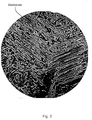
- FIG. 2 and 3 of the drawing show examples of images of fine structures in a CaF 2 crystal wafer.
- the images obtained in transmitted light with polarized monochromatic laser light each show the stress birefringence in the material disk. In principle, other wavelengths can also be used.
- FIG. 2 shows a crystal disk with a number of sliding planes
- FIG. 3 shows a crystal disk with many small-angle grain boundaries. 2 are represented by the straight, band-like structures which run over a large part of the crystal cross section.
- 3 shows a crystal disk, which also has some sliding planes on the edge, but in the middle of this crystal disk irregular worm-like curls dominate, which represent small-angle grain boundaries.
- the method according to the invention it is also possible to use lenses, Prisms, rectangular plates, light rods, optical Manufacture windows and optical devices for DUV lithography.
- the method is therefore also used in particular for the production of steppers and excimer lasers and thus also for the production of integrated circuits as well as electronic Devices such as computers containing computer chips and other electronic devices that integrated chip-like Circuits included.
Abstract
Description
Claims (9)
- Verfahren zur Bestimmung lokaler Strukturen in optischen Materialien, insbesondere in Kristallen, dadurch gekennzeichnet, daß in einem ersten Schritt mittels divergentem Weisslicht eine visuelle Bestimmung von Schlieren im Material durchgeführt wird, in einem zweiten Schritt mittels polarisiertem Laserlicht anhand von Spannungsdoppelbrechung eine Bestimmung von lokalen Defekten und Strukturfehlern mit einer Ortsauflösung von mindestens 0,5 mm erfolgt, und daß in einem dritten Schritt eine interferometrische Bestimmung von Materialfehlern erfolgt.
- Verfahren nach Anspruch 1, dadurch gekennzeichnet, daß die Ortsauflösung im zweiten und/oder dritten Schritt höher als 0,2 mm ist.
- Verfahren nach einem der vorhergehenden Ansprüche, dadurch gekennzeichnet, daß die Ortsauflösung im zweiten und/oder dritten Schritt höher als 0,1 mm ist.
- Verfahren nach einem der vorhergehenden Ansprüche, dadurch gekennzeichnet, daß alle Messungen an einer Scheibe des optischen Materials mit einer polierten Oberfläche erfolgen.
- Verfahren nach einem der vorhergehenden Ansprüche, dadurch gekennzeichnet, daß das Material ein Glas oder ein Kristall, insbesondere ein Alkali- oder Erdalkalihalogenidkristall oder -oxidkristall ist.
- Verfahren nach einem der vorhergehenden Ansprüche, dadurch gekennzeichnet, daß das Material nur dann einer Messung gemäß dem zweiten oder dritten Schritt unterworfen wird, wenn es im vorhergehenden Schritt vorgegebene Mindestanforderungen bezüglich der Fehlerfreiheit erfüllt hat.
- Verfahren nach einem der vorhergehenden Ansprüche, dadurch gekennzeichnet, daß aus den Materialien mit entsprechend geringen lokalen Strukturen ein optisches Element hergestellt wird.
- Verfahren nach einem der vorhergehenden Ansprüche, dadurch gekennzeichnet, daß es zur Herstellung von Linsen, Prismen, optischen Fenstern sowie optischen Komponenten für die DUV-Lithographie, Steppern, Excimerlasern, Wafern, Computerchips, sowie integrierten Schaltungen und elektronischen Geräten, die solche Chips enthalten, verwendet wird.
- Optisches Element erhältlich mit dem Verfahren nach einem der Ansprüche 1 bis 8.
Applications Claiming Priority (2)
| Application Number | Priority Date | Filing Date | Title |
|---|---|---|---|
| DE10227345A DE10227345A1 (de) | 2002-06-19 | 2002-06-19 | Verfahren zur Bestimmung lokaler Strukturen in optischen Kristallen |
| DE10227345 | 2002-06-19 |
Publications (5)
| Publication Number | Publication Date |
|---|---|
| EP1376103A2 true EP1376103A2 (de) | 2004-01-02 |
| EP1376103A8 EP1376103A8 (de) | 2004-04-28 |
| EP1376103A3 EP1376103A3 (de) | 2004-07-21 |
| EP1376103A9 EP1376103A9 (de) | 2004-09-08 |
| EP1376103B1 EP1376103B1 (de) | 2006-07-26 |
Family
ID=29716543
Family Applications (1)
| Application Number | Title | Priority Date | Filing Date |
|---|---|---|---|
| EP03013754A Expired - Lifetime EP1376103B1 (de) | 2002-06-19 | 2003-06-17 | Verfahren zur Bestimmung lokaler Strukturen in optischen Kristallen |
Country Status (5)
| Country | Link |
|---|---|
| US (1) | US6989904B2 (de) |
| EP (1) | EP1376103B1 (de) |
| JP (1) | JP4260555B2 (de) |
| AT (1) | ATE334385T1 (de) |
| DE (2) | DE10227345A1 (de) |
Families Citing this family (7)
| Publication number | Priority date | Publication date | Assignee | Title |
|---|---|---|---|---|
| WO2005080948A1 (en) * | 2004-02-23 | 2005-09-01 | Schott Ag | Process for preparing caf2 lens blanks especially for 193 nm and 157 nm lithography with minimized defects |
| DE102004060721B4 (de) * | 2004-12-17 | 2008-07-10 | Carl Zeiss Smt Ag | Verfahren zur Auswahl von optischen Materialien |
| WO2006114705A1 (en) * | 2005-04-27 | 2006-11-02 | Warner-Lambert Company Llc | Automated birefringence analysis and targeting system |
| DE102008001291B3 (de) * | 2008-04-21 | 2009-07-09 | Schott Ag | Hochpräzises Messverfahren zur Bestimmung von Materialspannungen |
| US10646315B2 (en) * | 2008-12-30 | 2020-05-12 | Ultradent Products, Inc. | Dental curing light having unibody design that acts as a heat sink |
| JP6536185B2 (ja) * | 2014-06-13 | 2019-07-03 | 信越化学工業株式会社 | 合成石英ガラス基板の製造方法 |
| JP6536192B2 (ja) * | 2015-06-10 | 2019-07-03 | 信越化学工業株式会社 | 合成石英ガラス基板の製造方法 |
Citations (2)
| Publication number | Priority date | Publication date | Assignee | Title |
|---|---|---|---|---|
| US3468610A (en) * | 1966-05-10 | 1969-09-23 | Muffoletto Carl V | Schlieren and strain birefringence system |
| DE19501158C1 (de) * | 1995-01-06 | 1996-04-11 | Oeg Ges Fuer Optik Elektronik | Vorrichtung zur Homogenitätsprüfung von optischen Gläsern und Kristallen |
Family Cites Families (9)
| Publication number | Priority date | Publication date | Assignee | Title |
|---|---|---|---|---|
| ATE116448T1 (de) * | 1989-06-09 | 1995-01-15 | Heraeus Quarzglas | Optische teile und rohlinge aus synthetischem siliziumdioxidglas und verfahren zu ihrer herstellung. |
| KR0165695B1 (ko) * | 1991-06-29 | 1998-12-15 | 아이하라 테루히코 | 엑시머레이저용 합성석영유리 광학부재 및 그의 제조방법 |
| JP3194667B2 (ja) * | 1994-03-26 | 2001-07-30 | 信越石英株式会社 | 光学用合成石英ガラス成形体及びその製造方法 |
| DE4434473A1 (de) * | 1994-09-27 | 1996-03-28 | Basler Gmbh | Verfahren und Vorrichtung zur Qualitätskontrolle von Gegenständen mit polarisiertem Licht |
| DE19626261A1 (de) * | 1995-06-30 | 1997-01-02 | Nikon Corp | Beobachtungsvorrichtung |
| WO1997026529A1 (en) * | 1996-01-19 | 1997-07-24 | Phase Metrics | Surface inspection apparatus and method |
| DE69801731T2 (de) * | 1997-03-25 | 2002-07-04 | Heraeus Quarzglas | Optisches system zur herstellung integrierter schaltungen |
| DE10005051B4 (de) * | 1999-11-15 | 2004-05-06 | Heraeus Quarzglas Gmbh & Co. Kg | Quarzglaskörper für ein optisches Bauteil, Verfahren zu seiner Herstellung und seine Verwendung |
| DE10111450B4 (de) * | 2001-03-09 | 2005-02-10 | Schott Ag | Verfahren und Vorrichtung zur Bewertung von Schlieren |
-
2002
- 2002-06-19 DE DE10227345A patent/DE10227345A1/de not_active Ceased
-
2003
- 2003-06-17 DE DE50304338T patent/DE50304338D1/de not_active Expired - Lifetime
- 2003-06-17 AT AT03013754T patent/ATE334385T1/de not_active IP Right Cessation
- 2003-06-17 EP EP03013754A patent/EP1376103B1/de not_active Expired - Lifetime
- 2003-06-18 US US10/464,402 patent/US6989904B2/en not_active Expired - Fee Related
- 2003-06-19 JP JP2003174243A patent/JP4260555B2/ja not_active Expired - Fee Related
Patent Citations (2)
| Publication number | Priority date | Publication date | Assignee | Title |
|---|---|---|---|---|
| US3468610A (en) * | 1966-05-10 | 1969-09-23 | Muffoletto Carl V | Schlieren and strain birefringence system |
| DE19501158C1 (de) * | 1995-01-06 | 1996-04-11 | Oeg Ges Fuer Optik Elektronik | Vorrichtung zur Homogenitätsprüfung von optischen Gläsern und Kristallen |
Non-Patent Citations (2)
| Title |
|---|
| ENGEL A ET AL: "Present and future industrial metrology needs for qualification of high-quality optical microlithography materials" OPTICAL METROLOGY ROADMAP FOR THE SEMICONDUCTOR, OPTICAL, AND DATA STORAGE INDUSTRIES II, SAN DIEGO, CA, USA, 2-3 AUG. 2001, Bd. 4449, Seiten 1-6, XP002280119 Proceedings of the SPIE - The International Society for Optical Engineering, 2001, SPIE-Int. Soc. Opt. Eng, USA ISSN: 0277-786X * |
| NISHIDA Y ET AL: "Development of a two-dimensional birefringence distribution measurement system in laser-diode pumped solid-state laser material" REVIEW OF SCIENTIFIC INSTRUMENTS, MAY 2001, AIP, USA, Bd. 72, Nr. 5, Seiten 2387-2391, XP002280120 ISSN: 0034-6748 * |
Also Published As
| Publication number | Publication date |
|---|---|
| DE50304338D1 (de) | 2006-09-07 |
| EP1376103A9 (de) | 2004-09-08 |
| ATE334385T1 (de) | 2006-08-15 |
| US6989904B2 (en) | 2006-01-24 |
| EP1376103B1 (de) | 2006-07-26 |
| US20040021803A1 (en) | 2004-02-05 |
| JP4260555B2 (ja) | 2009-04-30 |
| DE10227345A1 (de) | 2004-01-15 |
| EP1376103A8 (de) | 2004-04-28 |
| JP2004132953A (ja) | 2004-04-30 |
| EP1376103A3 (de) | 2004-07-21 |
Similar Documents
| Publication | Publication Date | Title |
|---|---|---|
| DE102010047050B4 (de) | Verfahren zur Charakterisierung einer Struktur auf einer Maske und Vorrichtung zur Durchführung des Verfahrens | |
| EP0019088A1 (de) | Ellipsometrisches Verfahren und ellipsometrische Vorrichtung zur Untersuchung der physikalischen Eigenschaften der Oberfläche einer Probe | |
| DE102009043001A1 (de) | Verfahren zur Bestimmung von Defekten in einem Für elektromagnetische Wellen transparenten Material, insbesonders für optische Zwecke, eine Vorrichtung hierzusowie die Verwendung dieser Materialien | |
| DE10111450B4 (de) | Verfahren und Vorrichtung zur Bewertung von Schlieren | |
| DE102005025535A1 (de) | Vorrichtung und Verfahren zur Verbesserung der Messgenauigkeit bei der Bestimmung von Strukturdaten | |
| DE10033645A1 (de) | Spektralellipsometer mit einer refraktiven Beleuchtungsoptik | |
| DE102011121532A1 (de) | Verfahren zur Charakterisierung einer Struktur auf einer Maske und Vorrichtung zur Durchführung des Verfahrens | |
| DE102018209175A1 (de) | Computer-generiertes Hologramm (CGH), sowie Verfahren zur Charakterisierung der Oberflächenform eines optischen Elements | |
| DE102012011315B4 (de) | Mikroskop und Verfahren zur Charakterisierung von Strukturen auf einem Objekt | |
| DE102007032626A1 (de) | Vorrichtung und Verfahren zur Verbesserung der Messgenauigkeit in einem optischen CD-Messsystem | |
| EP3134726B1 (de) | Verfahren und vorrichtung zum erkennen von nickelsulfid-einschlüssen in einer glasplatte | |
| EP1376103B1 (de) | Verfahren zur Bestimmung lokaler Strukturen in optischen Kristallen | |
| DE102012005417B4 (de) | Vorrichtung und Verfahren zur winkelaufgelösten Streulichtmessung | |
| DE10239330A1 (de) | Verfahren zur Herstellung von optischen Fluorid-Kristall-Lithographie/Laser-Elementen für Wellen-Längen <200 NM | |
| DE3931213C2 (de) | ||
| EP1552281B1 (de) | Bestimmung der eignung eines optischen materials zur herstellung von optischen elementen, eine vorrichtung hierzu und die verwendung des materials | |
| DE4211467C2 (de) | Verfahren zur Bestimmung räumlicher Anisotropiezustände eines niedrig orientierten zweiachsigen Objektes | |
| DE3218571A1 (de) | Verfahren und vorrichtung zur qualitativen und quantitativen bestimmung von unebenheiten und verunreinigungen auf und in transparenten oder semitransparenten flexiblen flaechengebilden | |
| EP3324149A1 (de) | Verfahren und vorrichtung zur bestimmung von oberflächenmodifikationen auf optisch transparenten bauteilen | |
| EP0508558B1 (de) | Apparat für ellipsometrische Untersuchungen von Materialien | |
| DE102008009044B4 (de) | Verfahren zur Messung der Dispersion von Phasenobjekten | |
| DE4444165A1 (de) | Vorrichtung zur Prüfung transparenter und/oder einseitig optisch undurchsichtig beschichteter Objekte auf Materialfehler | |
| DE10127508A1 (de) | Verfahren zur Bestimmung der Doppelbrechung optischer Materialien mit hoher Ortsauflösung | |
| DE4102731B4 (de) | Lithographieeinrichtung zum direkten Beschreiben eines Subtrates | |
| DE102004008750B4 (de) | Verfahren zur Qualitätskontrolle der optischen Eigenschaften eines optischen Materials mittels Bestimmung der Brechwerte |
Legal Events
| Date | Code | Title | Description |
|---|---|---|---|
| PUAI | Public reference made under article 153(3) epc to a published international application that has entered the european phase |
Free format text: ORIGINAL CODE: 0009012 |
|
| 17P | Request for examination filed |
Effective date: 20030617 |
|
| AK | Designated contracting states |
Kind code of ref document: A2 Designated state(s): AT BE BG CH CY CZ DE DK EE ES FI FR GB GR HU IE IT LI LU MC NL PT RO SE SI SK TR |
|
| AX | Request for extension of the european patent |
Extension state: AL LT LV MK |
|
| RAP1 | Party data changed (applicant data changed or rights of an application transferred) |
Owner name: SCHOTT GLAS Owner name: CARL ZEISS STIFTUNG TRADING AS SCHOTT GLASWERKE |
|
| PUAL | Search report despatched |
Free format text: ORIGINAL CODE: 0009013 |
|
| RIC1 | Information provided on ipc code assigned before grant |
Ipc: 7G 01N 21/896 A Ipc: 7G 01N 21/23 B Ipc: 7G 01N 21/45 B |
|
| AK | Designated contracting states |
Kind code of ref document: A3 Designated state(s): AT BE BG CH CY CZ DE DK EE ES FI FR GB GR HU IE IT LI LU MC NL PT RO SE SI SK TR |
|
| AX | Request for extension of the european patent |
Extension state: AL LT LV MK |
|
| RAP1 | Party data changed (applicant data changed or rights of an application transferred) |
Owner name: SCHOTT GLAS Owner name: CARL-ZEISS-STIFTUNGTRADING AS SCHOTT GLAS |
|
| RAP1 | Party data changed (applicant data changed or rights of an application transferred) |
Owner name: CARL-ZEISS-STIFTUNG TRADING AS SCHOTT GLAS Owner name: SCHOTT GLAS |
|
| RAP1 | Party data changed (applicant data changed or rights of an application transferred) |
Owner name: SCHOTT AG |
|
| 17Q | First examination report despatched |
Effective date: 20041203 |
|
| AKX | Designation fees paid |
Designated state(s): AT BE BG CH CY CZ DE DK EE ES FI FR GB GR HU IE IT LI LU MC NL PT RO SE SI SK TR |
|
| GRAP | Despatch of communication of intention to grant a patent |
Free format text: ORIGINAL CODE: EPIDOSNIGR1 |
|
| GRAS | Grant fee paid |
Free format text: ORIGINAL CODE: EPIDOSNIGR3 |
|
| GRAA | (expected) grant |
Free format text: ORIGINAL CODE: 0009210 |
|
| AK | Designated contracting states |
Kind code of ref document: B1 Designated state(s): AT BE BG CH CY CZ DE DK EE ES FI FR GB GR HU IE IT LI LU MC NL PT RO SE SI SK TR |
|
| PG25 | Lapsed in a contracting state [announced via postgrant information from national office to epo] |
Ref country code: IT Free format text: LAPSE BECAUSE OF FAILURE TO SUBMIT A TRANSLATION OF THE DESCRIPTION OR TO PAY THE FEE WITHIN THE PRESCRIBED TIME-LIMIT;WARNING: LAPSES OF ITALIAN PATENTS WITH EFFECTIVE DATE BEFORE 2007 MAY HAVE OCCURRED AT ANY TIME BEFORE 2007. THE CORRECT EFFECTIVE DATE MAY BE DIFFERENT FROM THE ONE RECORDED. Effective date: 20060726 Ref country code: IE Free format text: LAPSE BECAUSE OF FAILURE TO SUBMIT A TRANSLATION OF THE DESCRIPTION OR TO PAY THE FEE WITHIN THE PRESCRIBED TIME-LIMIT Effective date: 20060726 Ref country code: SK Free format text: LAPSE BECAUSE OF FAILURE TO SUBMIT A TRANSLATION OF THE DESCRIPTION OR TO PAY THE FEE WITHIN THE PRESCRIBED TIME-LIMIT Effective date: 20060726 Ref country code: RO Free format text: LAPSE BECAUSE OF FAILURE TO SUBMIT A TRANSLATION OF THE DESCRIPTION OR TO PAY THE FEE WITHIN THE PRESCRIBED TIME-LIMIT Effective date: 20060726 Ref country code: CZ Free format text: LAPSE BECAUSE OF FAILURE TO SUBMIT A TRANSLATION OF THE DESCRIPTION OR TO PAY THE FEE WITHIN THE PRESCRIBED TIME-LIMIT Effective date: 20060726 Ref country code: SI Free format text: LAPSE BECAUSE OF FAILURE TO SUBMIT A TRANSLATION OF THE DESCRIPTION OR TO PAY THE FEE WITHIN THE PRESCRIBED TIME-LIMIT Effective date: 20060726 Ref country code: FI Free format text: LAPSE BECAUSE OF FAILURE TO SUBMIT A TRANSLATION OF THE DESCRIPTION OR TO PAY THE FEE WITHIN THE PRESCRIBED TIME-LIMIT Effective date: 20060726 |
|
| REG | Reference to a national code |
Ref country code: GB Ref legal event code: FG4D Free format text: NOT ENGLISH |
|
| REG | Reference to a national code |
Ref country code: CH Ref legal event code: EP |
|
| REG | Reference to a national code |
Ref country code: IE Ref legal event code: FG4D Free format text: LANGUAGE OF EP DOCUMENT: GERMAN |
|
| REF | Corresponds to: |
Ref document number: 50304338 Country of ref document: DE Date of ref document: 20060907 Kind code of ref document: P |
|
| PG25 | Lapsed in a contracting state [announced via postgrant information from national office to epo] |
Ref country code: SE Free format text: LAPSE BECAUSE OF FAILURE TO SUBMIT A TRANSLATION OF THE DESCRIPTION OR TO PAY THE FEE WITHIN THE PRESCRIBED TIME-LIMIT Effective date: 20061026 Ref country code: DK Free format text: LAPSE BECAUSE OF FAILURE TO SUBMIT A TRANSLATION OF THE DESCRIPTION OR TO PAY THE FEE WITHIN THE PRESCRIBED TIME-LIMIT Effective date: 20061026 Ref country code: BG Free format text: LAPSE BECAUSE OF FAILURE TO SUBMIT A TRANSLATION OF THE DESCRIPTION OR TO PAY THE FEE WITHIN THE PRESCRIBED TIME-LIMIT Effective date: 20061026 |
|
| PG25 | Lapsed in a contracting state [announced via postgrant information from national office to epo] |
Ref country code: ES Free format text: LAPSE BECAUSE OF FAILURE TO SUBMIT A TRANSLATION OF THE DESCRIPTION OR TO PAY THE FEE WITHIN THE PRESCRIBED TIME-LIMIT Effective date: 20061106 |
|
| GBT | Gb: translation of ep patent filed (gb section 77(6)(a)/1977) |
Effective date: 20061016 |
|
| PG25 | Lapsed in a contracting state [announced via postgrant information from national office to epo] |
Ref country code: PT Free format text: LAPSE BECAUSE OF FAILURE TO SUBMIT A TRANSLATION OF THE DESCRIPTION OR TO PAY THE FEE WITHIN THE PRESCRIBED TIME-LIMIT Effective date: 20061226 |
|
| ET | Fr: translation filed | ||
| REG | Reference to a national code |
Ref country code: IE Ref legal event code: FD4D |
|
| PLBE | No opposition filed within time limit |
Free format text: ORIGINAL CODE: 0009261 |
|
| STAA | Information on the status of an ep patent application or granted ep patent |
Free format text: STATUS: NO OPPOSITION FILED WITHIN TIME LIMIT |
|
| 26N | No opposition filed |
Effective date: 20070427 |
|
| BERE | Be: lapsed |
Owner name: SCHOTT A.G. Effective date: 20070630 |
|
| PG25 | Lapsed in a contracting state [announced via postgrant information from national office to epo] |
Ref country code: MC Free format text: LAPSE BECAUSE OF NON-PAYMENT OF DUE FEES Effective date: 20070630 |
|
| REG | Reference to a national code |
Ref country code: CH Ref legal event code: PL |
|
| PG25 | Lapsed in a contracting state [announced via postgrant information from national office to epo] |
Ref country code: BE Free format text: LAPSE BECAUSE OF NON-PAYMENT OF DUE FEES Effective date: 20070630 |
|
| PG25 | Lapsed in a contracting state [announced via postgrant information from national office to epo] |
Ref country code: CH Free format text: LAPSE BECAUSE OF NON-PAYMENT OF DUE FEES Effective date: 20070630 Ref country code: GR Free format text: LAPSE BECAUSE OF FAILURE TO SUBMIT A TRANSLATION OF THE DESCRIPTION OR TO PAY THE FEE WITHIN THE PRESCRIBED TIME-LIMIT Effective date: 20061027 Ref country code: LI Free format text: LAPSE BECAUSE OF NON-PAYMENT OF DUE FEES Effective date: 20070630 |
|
| PG25 | Lapsed in a contracting state [announced via postgrant information from national office to epo] |
Ref country code: EE Free format text: LAPSE BECAUSE OF FAILURE TO SUBMIT A TRANSLATION OF THE DESCRIPTION OR TO PAY THE FEE WITHIN THE PRESCRIBED TIME-LIMIT Effective date: 20060726 |
|
| PG25 | Lapsed in a contracting state [announced via postgrant information from national office to epo] |
Ref country code: AT Free format text: LAPSE BECAUSE OF NON-PAYMENT OF DUE FEES Effective date: 20070617 |
|
| PG25 | Lapsed in a contracting state [announced via postgrant information from national office to epo] |
Ref country code: CY Free format text: LAPSE BECAUSE OF FAILURE TO SUBMIT A TRANSLATION OF THE DESCRIPTION OR TO PAY THE FEE WITHIN THE PRESCRIBED TIME-LIMIT Effective date: 20060726 Ref country code: LU Free format text: LAPSE BECAUSE OF NON-PAYMENT OF DUE FEES Effective date: 20070617 |
|
| PG25 | Lapsed in a contracting state [announced via postgrant information from national office to epo] |
Ref country code: TR Free format text: LAPSE BECAUSE OF FAILURE TO SUBMIT A TRANSLATION OF THE DESCRIPTION OR TO PAY THE FEE WITHIN THE PRESCRIBED TIME-LIMIT Effective date: 20060726 Ref country code: HU Free format text: LAPSE BECAUSE OF FAILURE TO SUBMIT A TRANSLATION OF THE DESCRIPTION OR TO PAY THE FEE WITHIN THE PRESCRIBED TIME-LIMIT Effective date: 20070127 |
|
| REG | Reference to a national code |
Ref country code: GB Ref legal event code: 732E Free format text: REGISTERED BETWEEN 20101007 AND 20101013 |
|
| REG | Reference to a national code |
Ref country code: FR Ref legal event code: TP |
|
| REG | Reference to a national code |
Ref country code: NL Ref legal event code: SD Effective date: 20110308 |
|
| PGFP | Annual fee paid to national office [announced via postgrant information from national office to epo] |
Ref country code: NL Payment date: 20120628 Year of fee payment: 10 |
|
| PGFP | Annual fee paid to national office [announced via postgrant information from national office to epo] |
Ref country code: FR Payment date: 20120705 Year of fee payment: 10 Ref country code: GB Payment date: 20120621 Year of fee payment: 10 |
|
| PGFP | Annual fee paid to national office [announced via postgrant information from national office to epo] |
Ref country code: DE Payment date: 20120827 Year of fee payment: 10 |
|
| REG | Reference to a national code |
Ref country code: NL Ref legal event code: V1 Effective date: 20140101 |
|
| GBPC | Gb: european patent ceased through non-payment of renewal fee |
Effective date: 20130617 |
|
| REG | Reference to a national code |
Ref country code: DE Ref legal event code: R119 Ref document number: 50304338 Country of ref document: DE Effective date: 20140101 |
|
| REG | Reference to a national code |
Ref country code: FR Ref legal event code: ST Effective date: 20140228 |
|
| PG25 | Lapsed in a contracting state [announced via postgrant information from national office to epo] |
Ref country code: GB Free format text: LAPSE BECAUSE OF NON-PAYMENT OF DUE FEES Effective date: 20130617 Ref country code: NL Free format text: LAPSE BECAUSE OF NON-PAYMENT OF DUE FEES Effective date: 20140101 Ref country code: DE Free format text: LAPSE BECAUSE OF NON-PAYMENT OF DUE FEES Effective date: 20140101 |
|
| PG25 | Lapsed in a contracting state [announced via postgrant information from national office to epo] |
Ref country code: FR Free format text: LAPSE BECAUSE OF NON-PAYMENT OF DUE FEES Effective date: 20130701 |