EP1367575B1 - Mehrstrahlige Halbleiterlasereinheit und optische Kopfanordnung - Google Patents
Mehrstrahlige Halbleiterlasereinheit und optische Kopfanordnung Download PDFInfo
- Publication number
- EP1367575B1 EP1367575B1 EP02256106A EP02256106A EP1367575B1 EP 1367575 B1 EP1367575 B1 EP 1367575B1 EP 02256106 A EP02256106 A EP 02256106A EP 02256106 A EP02256106 A EP 02256106A EP 1367575 B1 EP1367575 B1 EP 1367575B1
- Authority
- EP
- European Patent Office
- Prior art keywords
- semiconductor laser
- astigmatism
- elements
- laser elements
- objective lens
- Prior art date
- Legal status (The legal status is an assumption and is not a legal conclusion. Google has not performed a legal analysis and makes no representation as to the accuracy of the status listed.)
- Expired - Lifetime
Links
Images







Classifications
-
- G—PHYSICS
- G11—INFORMATION STORAGE
- G11B—INFORMATION STORAGE BASED ON RELATIVE MOVEMENT BETWEEN RECORD CARRIER AND TRANSDUCER
- G11B7/00—Recording or reproducing by optical means, e.g. recording using a thermal beam of optical radiation by modifying optical properties or the physical structure, reproducing using an optical beam at lower power by sensing optical properties; Record carriers therefor
- G11B7/12—Heads, e.g. forming of the optical beam spot or modulation of the optical beam
- G11B7/125—Optical beam sources therefor, e.g. laser control circuitry specially adapted for optical storage devices; Modulators, e.g. means for controlling the size or intensity of optical spots or optical traces
- G11B7/127—Lasers; Multiple laser arrays
- G11B7/1275—Two or more lasers having different wavelengths
-
- G—PHYSICS
- G11—INFORMATION STORAGE
- G11B—INFORMATION STORAGE BASED ON RELATIVE MOVEMENT BETWEEN RECORD CARRIER AND TRANSDUCER
- G11B7/00—Recording or reproducing by optical means, e.g. recording using a thermal beam of optical radiation by modifying optical properties or the physical structure, reproducing using an optical beam at lower power by sensing optical properties; Record carriers therefor
- G11B7/08—Disposition or mounting of heads or light sources relatively to record carriers
- G11B7/082—Aligning the head or the light source relative to the record carrier otherwise than during transducing, e.g. adjusting tilt set screw during assembly of head
-
- G—PHYSICS
- G11—INFORMATION STORAGE
- G11B—INFORMATION STORAGE BASED ON RELATIVE MOVEMENT BETWEEN RECORD CARRIER AND TRANSDUCER
- G11B7/00—Recording or reproducing by optical means, e.g. recording using a thermal beam of optical radiation by modifying optical properties or the physical structure, reproducing using an optical beam at lower power by sensing optical properties; Record carriers therefor
- G11B7/12—Heads, e.g. forming of the optical beam spot or modulation of the optical beam
- G11B7/22—Apparatus or processes for the manufacture of optical heads, e.g. assembly
-
- H—ELECTRICITY
- H01—ELECTRIC ELEMENTS
- H01S—DEVICES USING THE PROCESS OF LIGHT AMPLIFICATION BY STIMULATED EMISSION OF RADIATION [LASER] TO AMPLIFY OR GENERATE LIGHT; DEVICES USING STIMULATED EMISSION OF ELECTROMAGNETIC RADIATION IN WAVE RANGES OTHER THAN OPTICAL
- H01S5/00—Semiconductor lasers
- H01S5/02—Structural details or components not essential to laser action
- H01S5/022—Mountings; Housings
- H01S5/02208—Mountings; Housings characterised by the shape of the housings
- H01S5/02212—Can-type, e.g. TO-CAN housings with emission along or parallel to symmetry axis
-
- H—ELECTRICITY
- H01—ELECTRIC ELEMENTS
- H01S—DEVICES USING THE PROCESS OF LIGHT AMPLIFICATION BY STIMULATED EMISSION OF RADIATION [LASER] TO AMPLIFY OR GENERATE LIGHT; DEVICES USING STIMULATED EMISSION OF ELECTROMAGNETIC RADIATION IN WAVE RANGES OTHER THAN OPTICAL
- H01S5/00—Semiconductor lasers
- H01S5/02—Structural details or components not essential to laser action
- H01S5/022—Mountings; Housings
- H01S5/0225—Out-coupling of light
- H01S5/02257—Out-coupling of light using windows, e.g. specially adapted for back-reflecting light to a detector inside the housing
-
- H—ELECTRICITY
- H01—ELECTRIC ELEMENTS
- H01S—DEVICES USING THE PROCESS OF LIGHT AMPLIFICATION BY STIMULATED EMISSION OF RADIATION [LASER] TO AMPLIFY OR GENERATE LIGHT; DEVICES USING STIMULATED EMISSION OF ELECTROMAGNETIC RADIATION IN WAVE RANGES OTHER THAN OPTICAL
- H01S5/00—Semiconductor lasers
- H01S5/02—Structural details or components not essential to laser action
- H01S5/022—Mountings; Housings
- H01S5/0235—Method for mounting laser chips
- H01S5/02375—Positioning of the laser chips
-
- H—ELECTRICITY
- H01—ELECTRIC ELEMENTS
- H01S—DEVICES USING THE PROCESS OF LIGHT AMPLIFICATION BY STIMULATED EMISSION OF RADIATION [LASER] TO AMPLIFY OR GENERATE LIGHT; DEVICES USING STIMULATED EMISSION OF ELECTROMAGNETIC RADIATION IN WAVE RANGES OTHER THAN OPTICAL
- H01S5/00—Semiconductor lasers
- H01S5/40—Arrangement of two or more semiconductor lasers, not provided for in groups H01S5/02 - H01S5/30
- H01S5/4025—Array arrangements, e.g. constituted by discrete laser diodes or laser bar
- H01S5/4031—Edge-emitting structures
-
- H—ELECTRICITY
- H01—ELECTRIC ELEMENTS
- H01S—DEVICES USING THE PROCESS OF LIGHT AMPLIFICATION BY STIMULATED EMISSION OF RADIATION [LASER] TO AMPLIFY OR GENERATE LIGHT; DEVICES USING STIMULATED EMISSION OF ELECTROMAGNETIC RADIATION IN WAVE RANGES OTHER THAN OPTICAL
- H01S5/00—Semiconductor lasers
- H01S5/40—Arrangement of two or more semiconductor lasers, not provided for in groups H01S5/02 - H01S5/30
- H01S5/4025—Array arrangements, e.g. constituted by discrete laser diodes or laser bar
- H01S5/4087—Array arrangements, e.g. constituted by discrete laser diodes or laser bar emitting more than one wavelength
Definitions
- An optical head device has been widely used for recording to or reproducing from an optical disk such as a DVD (Digital Versatile Disc), a CD (Compact Disc) or the like.
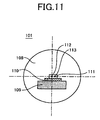
- An optical head device 100 shown in Fig. 10, which is a conventional example, is equipped with a conventional semiconductor laser unit 101 capable of emitting a plurality of laser beams, so-called a multi-beam semiconductor laser unit.
- a half mirror 102 is arranged on a light-emission side of the semiconductor laser unit 101.
- a collimator lens 103 and an objective lens 104 are arranged in the order on a light-reflection side of the half mirror 102.
- an optical disk 105 or 106 is arranged to record thereto or reproduce therefrom.
- the focal spot 15 is formed on the optical axis 17 of the objective lens 10 whereas the other focal spot 17 is formed off the optical axis 7.
- the two focal spots 15 and 17 are different in focal state due to so-called an image height characteristic of the objective lens 10. This will be explained using Fig. 3.
- Embodiment 3 shows the case using the multi-beam semiconductor laser unit 3 having the semiconductor laser elements 4, 5 shown in Embodiment 1, the cover glass 25 used in Embodiment 3 may also be applied to a multi-beam semiconductor laser unit 18 having the semiconductor laser elements 19, 20 shown in Embodiment 2.
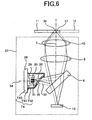
- references 7 to 13 are the same as those shown in Fig. 1.
- a semiconductor laser unit 28 is capable of emitting a plurality of laser beams, showing herein a unit mounted with a monolithically integrated multi-beam semiconductor laser unit 29.
- the multi-beam semiconductor laser unit 29 includes semiconductor laser elements 30 and 31.
- the two semiconductor laser elements 30 and 31 have the same astigmatism.
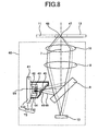
- the astigmatism existing on the semiconductor laser element 43 is greater than that on the semiconductor laser element 44, the astigmatism is not completely canceled by the light transmission through the cover glass 49, to propagate a laser beam 45 having an astigmatism partly remained.
- This laser beam 45 is coincident in its axis with the optical axis 7, and therefore, it is focused without the influence of an image height characteristic of the objective lens 10.
- a cover glass 59 in a parallel plate form is fixed on the case T62 of the base T6, with inclination relative to the laser beam-emitting surface of the semiconductor laser elements 53, 54.
- the refractive index and thickness of the cover glass 59 and the inclination angle to the laser beam-emitting surface for laser beams 53, 54 are set to cancel the astigmatism inherently existing on the semiconductor laser element 53.
- the cover glass 59 may be a synthetic-resin light transmissive member besides a glass-made one provided that it can compensate the astigmatism on the semiconductor laser element 53 greater in astigmatism. It is possible to use a cylindrical lens, a hologram, a Fresnel lens, a coupling lens or the like.
- the laser beams 55, 56 respectively emitted from the semiconductor laser elements 53, 54 transmit through the cover glass 59.
- the astigmatism existing on the semiconductor laser element 53 greater in astigmatism is canceled by transmission through the cover glass 59, to propagate a laser beam 55 compensated in astigmatism.
- the cover glass 59 together with the cover T62, serves to protect the multi-beam semiconductor laser unit 52 from dust and dirt or the oxygen in the air. Because the laser beam 55 after transmitted through the cover glass 59 is coincident in its axis with the optical axis 7 of the objective lens 10, it is focused without the influence of an image height characteristic of the objective lens 10, to form a focal spot 57. Namely, no astigmatism exists in the focal spot 57.
- the degree of cancellation depends upon a magnitude of the astigmatism inherently possessed by the semiconductor laser element 54 and the image height characteristic of the objective lens 10.
- the cancellation is possible to nearly zero by adjusting this astigmatism, this image height characteristic, and other conditions.
- the two focal spots 57, 58 can be provided with astigmatisms not existing at the same time. It is possible to provide a favorable focusing characteristic.
- the astigmatism is compensated through the cover glass 59. Furthermore, because the laser beam 55, after transmission through the cover glass 59, is propagated in an axis just on the optical axis 7, no astigmatism newly occurs. On the other hand, as for the laser beam 56 emitted from the semiconductor laser element 54 smaller in astigmatism, excessive compensation is made by the cover glass 59 to reverse the direction of astigmatism. Furthermore, because of propagation at a laser beam axis off the optical axis 7, an astigmatism newly occurs due to the image height characteristic of the objective lens 10. However, it is structurally possible to cancel between this astigmatism and the reverse astigmatism by the cover glass 59. Therefore, focusing characteristic evenness of the laser beams 55, 56 can be obtained.
Landscapes
- Physics & Mathematics (AREA)
- Optics & Photonics (AREA)
- Optical Head (AREA)
- Semiconductor Lasers (AREA)
Claims (12)
- Verfahren zur Herstellung einer optischen Kopfanordnung (27, 40, 50) zum Beschreiben eines optischen Mediums und/oder zum Wiedergeben von einem optischen Medium, wobei das Verfahren folgende Schritte umfasst:Ermitteln des Astigmatismus' eines jeden von mehreren Halbleiterlaserelementen;Anordnen der mehreren Halbleiterlaserelemente (4, 5, 43, 44, 53, 54) parallel zueinander in einer Laserstrahlaussenderichtung;Bereitstellen einer Objektivlinse (10) zum Richten von Laserstrahlen, die von den mehreren Halbleiterlaserelementen ausgesandt werden, auf das optische Medium; undBereitstellen eines Photodetektors zum Detektieren eines Laserstrahls, der auf das optische Medium gerichtet ist;wobei die mehreren Halbleiterlaserelemente dergestalt befestigt sind, dass während des Beschreibens oder Wiedergebens mittels eines beliebigen der Laserstrahlen der Pfad eines Laserstrahls, der von demjenigen Halbleiterlaserelement der mehreren Halbleiterlaserelemente ausgesandt wurde, das den größten Astigmatismus aufweist (4, 43), in seiner Achse mit einer optischen Achse der Objektivlinse übereinstimmt und der Pfad eines Laserstrahls von dem Halbleiterlaserelement, dessen Astigmatismus geringer ist, außerhalb der optischen Achse liegt.
- Verfahren zur Herstellung einer optischen Kopfanordnung (1) zum Beschreiben eines optischen Mediums und/oder zum Wiedergeben von einem optischen Medium, wobei das Verfahren folgende Schritte umfasst:Ermitteln des Astigmatismus' eines jeden von mehreren Halbleiterlaserelementen;Anordnen der mehreren Halbleiterlaserelemente (19, 20, 30, 31) parallel zueinander in einer Laserstrahlaussenderichtung, wobei wenigstens zwei der mehreren Halbleiterlaserelemente einen im Wesentlichen gleichen Astigmatismus aufweisen;Bereitstellen einer Objektivlinse (10) zum Richten von Laserstrahlen, die von den mehreren Halbleiterlaserelementen ausgesandt werden, auf das optische Medium; undBereitstellen eines Photodetektors (13) zum Detektieren eines Laserstrahls, der auf das optische Medium gerichtet ist;wobei die mehreren Halbleiterlaserelemente (19, 20, 30, 31) dergestalt befestigt sind, dass Achsen von Laserstrahlen, die von den wenigstens zwei Halbleiterlaserelementen ausgesandt wurden, eine optische Achse (7) der Objektivlinse (10) in die Mitte nehmen und um einen im Wesentlichen gleichen Abstand von der optischen Achse (7) beabstandet sind.
- Verfahren nach Anspruch 1 oder Anspruch 2, wobei des Weiteren zwischen den mehreren Halbleiterlaserelementen und der Objektivlinse ein lichtdurchlässiges Element in einer Parallelplattenform vor einer - und parallel zu einer - Laserstrahlaussendefläche der mehreren Halbleiterlaserelemente angeordnet ist.
- Verfahren zur Herstellung einer optischen Kopfanordnung (1) zum Beschreiben eines optischen Mediums und/oder zum Wiedergeben von einem optischen Medium, wobei das Verfahren folgende Schritte umfasst:Ermitteln des Astigmatismus' eines jeden von mehreren Halbleiterlaserelementen;Anordnen der mehreren Halbleiterlaserelemente (19, 20, 30, 31) parallel zueinander in einer Laserstrahlaussenderichtung, wobei wenigstens zwei der mehreren Halbleiterlaserelemente einen im Wesentlichen gleichen Astigmatismus aufweisen;Bereitstellen einer Objektivlinse (10) zum Richten von Laserstrahlen, die von den mehreren Halbleiterlaserelementen ausgesandt werden, auf das optische Medium; undBereitstellen eines Photodetektors (13) zum Detektieren eines Laserstrahls, der auf das optische Medium gerichtet ist;wobei die mehreren Halbleiterlaserelemente (19, 20, 30, 31) dergestalt befestigt sind, dass Achsen von Laserstrahlen, die von den wenigstens zwei Halbleiterlaserelementen ausgesandt wurden, eine optische Achse (7) der Objektivlinse (10) in die Mitte nehmen, wobei das Verfahren des Weiteren umfasst, einen Astigmatismuskompensator (35) vor einer Laserstrahlaussendefläche der mehreren Halbleiterlaserelemente anzuordnen, um einen Astigmatismus der wenigstens zwei Halbleiterlaserelemente (30, 31) zu kompensieren;
wobei die mehreren Halbleiterlaserelemente (30, 31) dergestalt befestigt sind, dass Achsen von Laserstrahlen, die von den wenigstens zwei Halbleiterlaserelementen ausgesandt wurden, nach dem Passieren des Astigmatismuskompensators eine optische Achse (7) der Objektivlinse (10) in die Mitte nehmen und um einen im Wesentlichen gleichen Abstand von der optischen Achse beabstandet sind. - Verfahren nach Anspruch 1, wobei:die mehreren Halbleiterlaserelemente ein erstes Halbleiterlaserelement (43) mit einem größten Astigmatismus und ein zweites Halbleiterlaserelement (44) mit einem kleineren Astigmatismus als das erste Halbleiterlaserelement umfassen;wobei das Verfahren des Weiteren den Schritt umfasst, einen Astigmatismuskompensator (49) vor einer Laserstrahlaussendefläche der mehreren Halbleiterlaserelemente anzuordnen, um einen Astigmatismus des zweiten Halbleiterlaserelements (44) zu kompensieren;
wobei die mehreren Halbleiterlaserelemente (43, 44) dergestalt angeordnet sind, dass ein Laserstrahl, der von dem ersten Halbleiterlaserelement (43) ausgesandt wird, nach dem Passieren des Astigmatismuskompensators (49) in seiner Achse mit einer optischen Achse (7) der Objektivlinse übereinstimmt. - Verfahren nach Anspruch 1, wobei:die mehreren Halbleiterlaserelemente ein erstes Halbleiterlaserelement (53) mit einem größten Astigmatismus und ein zweites Halbleiterlaserelement (54) mit einem kleineren Astigmatismus als das erste Halbleiterlaserelement umfassen;wobei das Verfahren des Weiteren den Schritt umfasst, einen Astigmatismuskompensator (59) vor einer Laserstrahlaussendefläche der mehreren Halbleiterlaserelemente anzuordnen, um einen Astigmatismus des ersten Halbleiterlaserelements (53) zu kompensieren;
wobei die mehreren Halbleiterlaserelemente (53, 54) dergestalt angeordnet sind, dass ein Laserstrahl, der von dem ersten Halbleiterlaserelement (53) ausgesandt wird, nach dem Passieren des Astigmatismuskompensators (59) in seiner Achse mit einer optischen Achse der Objektivlinse übereinstimmt. - Verfahren nach einem der Ansprüche 4 bis 6, wobei der Astigmatismuskompensator ein lichtdurchlässiges Element in einer Parallelplattenform ist, das mit einer Neigung relativ zu der Laserstrahlaussendefläche der mehreren Halbleiterlaserelemente angeordnet ist.
- Verfahren nach einem der Ansprüche 1 bis 7, wobei die mehreren Halbleiterlaserelemente Laserstrahlen von gleicher oder unterschiedlicher Wellenlänge aussenden.
- Optische Kopfanordnung (40) zum Beschreiben eines optischen Mediums und/oder zum Wiedergeben von einem optischen Medium, wobei die optische Kopfanordnung Folgendes umfasst:mehrere Halbleiterlaserelemente (43, 44), die parallel zueinander in einer Laserstrahlaussenderichtung angeordnet sind;
wobei die mehreren Halbleiterlaserelemente ein erstes Halbleiterlaserelement (43), das einen größten Astigmatismus aufweist, und ein zweites Halbleiterlaserelement (44), das einen kleineren Astigmatismus als das erste Halbleiterlaserelement aufweist, umfassen;eine Objektivlinse (10) zum Richten von Laserstrahlen, die von den mehreren Halbleiterlaserelementen ausgesandt werden, auf das optische Medium; undeinen Photodetektor zum Detektieren eines Laserstrahls, der auf das optische Medium gerichtet ist; undeinen Astigmatismuskompensator (49), der vor einer Laserstrahlaussendefläche der mehreren Halbleiterlaserelemente angeordnet ist, wobei dieser Astigmatismuskompensator einen Astigmatismus des zweiten Halbleiterlaserelements (44) kompensiert, aber nicht den Astigmatismus des ersten Halbleiterlaserelements vollständig beseitigt;wobei die mehreren Halbleiterlaserelemente (43, 44) dergestalt angeordnet sind, dass ein Laserstrahl, der von dem ersten Halbleiterlaserelement (43) ausgesandt wird, nach dem Passieren des Astigmatismuskompensators (49) in seiner Achse mit einer optischen Achse (7) der Objektivlinse übereinstimmt. - Optische Kopfanordnung (50) zum Beschreiben eines optischen Mediums und/oder zum Wiedergeben von einem optischen Medium, wobei die optische Kopfanordnung Folgendes umfasst:mehrere Halbleiterlaserelemente (53, 54), die parallel zueinander in einer Laserstrahlaussenderichtung angeordnet sind;
wobei die mehreren Halbleiterlaserelemente ein erstes Halbleiterlaserelement (53), das einen größten Astigmatismus aufweist, und ein zweites Halbleiterlaserelement (54), das einen kleineren Astigmatismus als das erste Halbleiterlaserelement aufweist, umfassen;eine Objektivlinse (10) zum Richten von Laserstrahlen, die von den mehreren Halbleiterlaserelementen ausgesandt werden, auf das optische Medium; undeinen Photodetektor zum Detektieren eines Laserstrahls, der auf das optische Medium gerichtet ist; undeinen Astigmatismuskompensator (59), der vor einer Laserstrahlaussendefläche der mehreren Halbleiterlaserelemente angeordnet ist, wobei dieser Astigmatismuskompensator (49) einen Astigmatismus des ersten Halbleiterlaserelements (53) kompensiert, aber nicht den Astigmatismus des zweiten Halbleiterlaserelements vollständig beseitigt;wobei die mehreren Halbleiterlaserelemente (53, 54) dergestalt angeordnet sind, dass ein Laserstrahl, der von dem ersten Halbleiterlaserelement (53) ausgesandt wird, nach dem Passieren des Astigmatismuskompensators (59) in seiner Achse mit einer optischen Achse der Objektivlinse übereinstimmt. - Optische Kopfanordnung nach Anspruch 9 oder Anspruch 10, wobei der Astigmatismuskompensator ein lichtdurchlässiges Element in einer Parallelplattenform ist, das mit einer Neigung relativ zu der Laserstrahlaussendefläche der mehreren Halbleiterlaserelemente angeordnet ist.
- Optische Kopfanordnung nach einem der Ansprüche 9 bis 11, wobei die mehreren Halbleiterlaserelemente Laserstrahlen von gleicher oder unterschiedlicher Wellenlänge aussenden.
Applications Claiming Priority (2)
| Application Number | Priority Date | Filing Date | Title |
|---|---|---|---|
| JP2002153799A JP3546877B2 (ja) | 2002-05-28 | 2002-05-28 | 半導体レーザ装置及び光ヘッド装置 |
| JP2002153799 | 2002-05-28 |
Publications (3)
| Publication Number | Publication Date |
|---|---|
| EP1367575A2 EP1367575A2 (de) | 2003-12-03 |
| EP1367575A3 EP1367575A3 (de) | 2004-12-22 |
| EP1367575B1 true EP1367575B1 (de) | 2006-12-20 |
Family
ID=29417169
Family Applications (1)
| Application Number | Title | Priority Date | Filing Date |
|---|---|---|---|
| EP02256106A Expired - Lifetime EP1367575B1 (de) | 2002-05-28 | 2002-09-03 | Mehrstrahlige Halbleiterlasereinheit und optische Kopfanordnung |
Country Status (5)
| Country | Link |
|---|---|
| US (2) | US6912192B2 (de) |
| EP (1) | EP1367575B1 (de) |
| JP (1) | JP3546877B2 (de) |
| CN (2) | CN100375173C (de) |
| DE (1) | DE60216896T2 (de) |
Families Citing this family (9)
| Publication number | Priority date | Publication date | Assignee | Title |
|---|---|---|---|---|
| JP2003152260A (ja) * | 2001-11-09 | 2003-05-23 | Sharp Corp | 半導体レーザ装置およびそれを用いた光ピックアップ装置、ならびに半導体レーザ装置の製造装置および製造方法 |
| JP3546877B2 (ja) * | 2002-05-28 | 2004-07-28 | 三菱電機株式会社 | 半導体レーザ装置及び光ヘッド装置 |
| JP4706481B2 (ja) * | 2003-12-25 | 2011-06-22 | コニカミノルタオプト株式会社 | 光ピックアップ装置 |
| JP4234697B2 (ja) * | 2005-06-15 | 2009-03-04 | 浜松ホトニクス株式会社 | レーザ装置 |
| US10088298B2 (en) | 2015-09-04 | 2018-10-02 | Kla-Tencor Corporation | Method of improving lateral resolution for height sensor using differential detection technology for semiconductor inspection and metrology |
| CN111007484B (zh) * | 2019-12-27 | 2023-08-25 | 联合微电子中心有限责任公司 | 一种单线激光雷达 |
| CN112025088B (zh) * | 2020-08-06 | 2022-04-15 | 武汉华工激光工程有限责任公司 | 一种激光光束像散补偿方法及激光加工系统 |
| CN114400500B (zh) * | 2021-12-28 | 2023-12-22 | 中国科学院光电技术研究所 | 一种激光外调制横模发生装置 |
| CN116937308B (zh) * | 2023-06-13 | 2025-10-28 | 深圳联品激光技术有限公司 | 脉冲激光器 |
Family Cites Families (26)
| Publication number | Priority date | Publication date | Assignee | Title |
|---|---|---|---|---|
| US6657931B1 (en) * | 1959-02-02 | 2003-12-02 | Sony Corporation | Optical disc drive for performing read/write operations on optical disks |
| JP4126799B2 (ja) * | 1999-03-03 | 2008-07-30 | ソニー株式会社 | 光ディスク装置 |
| CA1204199A (en) * | 1982-02-19 | 1986-05-06 | Shigeo Kubota | Optical apparatus |
| JPS61184735A (ja) | 1985-02-12 | 1986-08-18 | Nec Corp | マルチビ−ム型光ピツクアツプ装置 |
| US4942584A (en) * | 1988-06-22 | 1990-07-17 | Morihiro Karaki | Semiconductor laser apparatus driving system |
| JP2585761B2 (ja) | 1988-11-15 | 1997-02-26 | キヤノン株式会社 | 光ヘッド |
| JPH06274931A (ja) | 1993-01-22 | 1994-09-30 | Ricoh Co Ltd | 光ピックアップおよび光ピックアップにおけるビーム整形機能を有するカップリングレンズ |
| JP3778316B2 (ja) * | 1997-05-22 | 2006-05-24 | パイオニア株式会社 | 光ピックアップ装置 |
| KR20000009844A (ko) * | 1998-07-29 | 2000-02-15 | 사까이 히로시 | 광픽업 |
| JP2000348369A (ja) * | 1999-04-02 | 2000-12-15 | Ricoh Co Ltd | 光ピックアップ |
| JP2002025103A (ja) * | 2000-07-07 | 2002-01-25 | Toshiba Corp | 光学ヘッド装置 |
| JP2001176110A (ja) * | 1999-12-13 | 2001-06-29 | Alps Electric Co Ltd | 光ピックアップ装置 |
| JP2001184698A (ja) * | 1999-12-22 | 2001-07-06 | Pioneer Electronic Corp | 光ピックアップ装置 |
| JP3689296B2 (ja) * | 2000-01-24 | 2005-08-31 | パイオニア株式会社 | 光ピックアップ装置 |
| JP2001237501A (ja) | 2000-02-23 | 2001-08-31 | Rohm Co Ltd | 半導体レーザ装置の光軸アラインメント方法および半導体レーザ装置 |
| JP3859416B2 (ja) * | 2000-02-29 | 2006-12-20 | 株式会社日立製作所 | 対物レンズ、これを用いた光ヘッドおよび光ディスク装置 |
| JP2001298238A (ja) | 2000-04-14 | 2001-10-26 | Toshiba Corp | 光集積ユニット及び光ピックアップ装置 |
| JP2001331955A (ja) * | 2000-05-22 | 2001-11-30 | Matsushita Electric Ind Co Ltd | 光学ヘッド制御装置 |
| JP2001338432A (ja) * | 2000-05-25 | 2001-12-07 | Pioneer Electronic Corp | 光ピックアップ装置 |
| JP2002008258A (ja) * | 2000-06-21 | 2002-01-11 | Pioneer Electronic Corp | 光ピックアップ装置 |
| JP2002025096A (ja) * | 2000-07-07 | 2002-01-25 | Matsushita Electric Ind Co Ltd | 半導体光源、光ピックアップヘッド装置及び情報記録再生装置 |
| CN1287185C (zh) * | 2000-10-06 | 2006-11-29 | 宾得株式会社 | 用于光学头的物镜、光学头以及光盘驱动器 |
| JP2002163837A (ja) * | 2000-11-27 | 2002-06-07 | Pioneer Electronic Corp | 光ピックアップ装置及びレーザダイオードチップ |
| JP2003163405A (ja) * | 2001-11-26 | 2003-06-06 | Sony Corp | 2波長半導体レーザ素子およびそれに用いられる非点補正板ならびにその配置方法 |
| JP4205886B2 (ja) * | 2002-04-02 | 2009-01-07 | Hoya株式会社 | 光ヘッド用対物レンズ、これを用いた光ヘッドおよび光ディスク装置 |
| JP3546877B2 (ja) * | 2002-05-28 | 2004-07-28 | 三菱電機株式会社 | 半導体レーザ装置及び光ヘッド装置 |
-
2002
- 2002-05-28 JP JP2002153799A patent/JP3546877B2/ja not_active Expired - Lifetime
- 2002-09-03 EP EP02256106A patent/EP1367575B1/de not_active Expired - Lifetime
- 2002-09-03 DE DE60216896T patent/DE60216896T2/de not_active Expired - Lifetime
- 2002-09-11 US US10/238,581 patent/US6912192B2/en not_active Expired - Lifetime
- 2002-11-29 CN CNB200410100026XA patent/CN100375173C/zh not_active Expired - Lifetime
- 2002-11-29 CN CNB021529604A patent/CN1203599C/zh not_active Expired - Lifetime
-
2004
- 2004-11-01 US US10/976,811 patent/US7266072B2/en not_active Expired - Lifetime
Also Published As
| Publication number | Publication date |
|---|---|
| CN100375173C (zh) | 2008-03-12 |
| DE60216896D1 (de) | 2007-02-01 |
| EP1367575A2 (de) | 2003-12-03 |
| JP3546877B2 (ja) | 2004-07-28 |
| DE60216896T2 (de) | 2007-07-05 |
| CN1463060A (zh) | 2003-12-24 |
| HK1059009A1 (en) | 2004-06-11 |
| EP1367575A3 (de) | 2004-12-22 |
| US6912192B2 (en) | 2005-06-28 |
| US20030231670A1 (en) | 2003-12-18 |
| HK1077394A1 (zh) | 2006-02-10 |
| CN1624783A (zh) | 2005-06-08 |
| US20050094693A1 (en) | 2005-05-05 |
| US7266072B2 (en) | 2007-09-04 |
| JP2003347682A (ja) | 2003-12-05 |
| CN1203599C (zh) | 2005-05-25 |
Similar Documents
| Publication | Publication Date | Title |
|---|---|---|
| US7200098B2 (en) | Objective lens for high-density optical focusing and an optical disk in an optical pickup | |
| EP1096483B1 (de) | Optische Abtasteinheit | |
| KR100765741B1 (ko) | 일 매의 렌즈로 된 고개구수의 대물렌즈 및 이를 채용한광픽업장치 | |
| EP1367575B1 (de) | Mehrstrahlige Halbleiterlasereinheit und optische Kopfanordnung | |
| JPH1064103A (ja) | 光ピックアップ装置 | |
| EP1158502B1 (de) | Objektivlinse und damit ausgerüstete optische Abtastvorrichtung | |
| US8036093B2 (en) | Optical head device and recording/reproduction device | |
| JP2005512253A (ja) | 光走査デバイス | |
| US7525896B2 (en) | Optical head and optical disk apparatus | |
| JPH10321961A (ja) | 半導体レーザ装置 | |
| US7164626B2 (en) | Optical pickup using a wedge type beam splitter | |
| HK1077394B (en) | Semiconductor laser unit and optical head device | |
| JP4834168B2 (ja) | 光ピックアップ装置 | |
| KR100683888B1 (ko) | 광픽업 장치 | |
| JP2001209968A (ja) | 光記録媒体読み/書き用装置 | |
| US20110044155A1 (en) | Optical pickup device | |
| US7466643B2 (en) | Optical pickup system and information recording and/or reproducing apparatus employing the same | |
| JP3608046B2 (ja) | 光ディスク装置 | |
| JP2005535066A (ja) | レンズ保護デバイスを備えた対物系を含む走査デバイス | |
| JPH10302295A (ja) | 光ピックアップ装置 | |
| JP2001291267A (ja) | 光ピックアップ装置 | |
| KR20050030225A (ko) | 단일 물질로 이루어진 대물계를 구비한 주사장치 | |
| JPH11232685A (ja) | ビーム整形素子およびそれを用いた光ピックアップ | |
| KR20050047185A (ko) | 광 픽업 장치 | |
| JP2000089120A (ja) | 対物レンズ |
Legal Events
| Date | Code | Title | Description |
|---|---|---|---|
| PUAI | Public reference made under article 153(3) epc to a published international application that has entered the european phase |
Free format text: ORIGINAL CODE: 0009012 |
|
| AK | Designated contracting states |
Kind code of ref document: A2 Designated state(s): AT BE BG CH CY CZ DE DK EE ES FI FR GB GR IE IT LI LU MC NL PT SE SK TR |
|
| AX | Request for extension of the european patent |
Extension state: AL LT LV MK RO SI |
|
| PUAL | Search report despatched |
Free format text: ORIGINAL CODE: 0009013 |
|
| AK | Designated contracting states |
Kind code of ref document: A3 Designated state(s): AT BE BG CH CY CZ DE DK EE ES FI FR GB GR IE IT LI LU MC NL PT SE SK TR |
|
| AX | Request for extension of the european patent |
Extension state: AL LT LV MK RO SI |
|
| RIC1 | Information provided on ipc code assigned before grant |
Ipc: 7G 11B 7/125 A Ipc: 7G 11B 7/135 B Ipc: 7H 01S 5/40 B |
|
| 17P | Request for examination filed |
Effective date: 20050118 |
|
| 17Q | First examination report despatched |
Effective date: 20050304 |
|
| AKX | Designation fees paid |
Designated state(s): DE FR GB |
|
| GRAP | Despatch of communication of intention to grant a patent |
Free format text: ORIGINAL CODE: EPIDOSNIGR1 |
|
| RAP1 | Party data changed (applicant data changed or rights of an application transferred) |
Owner name: MITSUBISHI DENKI KABUSHIKI KAISHA |
|
| GRAS | Grant fee paid |
Free format text: ORIGINAL CODE: EPIDOSNIGR3 |
|
| GRAA | (expected) grant |
Free format text: ORIGINAL CODE: 0009210 |
|
| AK | Designated contracting states |
Kind code of ref document: B1 Designated state(s): DE FR GB |
|
| REG | Reference to a national code |
Ref country code: GB Ref legal event code: FG4D |
|
| REF | Corresponds to: |
Ref document number: 60216896 Country of ref document: DE Date of ref document: 20070201 Kind code of ref document: P |
|
| ET | Fr: translation filed | ||
| PLBE | No opposition filed within time limit |
Free format text: ORIGINAL CODE: 0009261 |
|
| STAA | Information on the status of an ep patent application or granted ep patent |
Free format text: STATUS: NO OPPOSITION FILED WITHIN TIME LIMIT |
|
| 26N | No opposition filed |
Effective date: 20070921 |
|
| REG | Reference to a national code |
Ref country code: GB Ref legal event code: 746 Effective date: 20110513 |
|
| REG | Reference to a national code |
Ref country code: DE Ref legal event code: R084 Ref document number: 60216896 Country of ref document: DE Effective date: 20110629 Ref country code: DE Ref legal event code: R084 Ref document number: 60216896 Country of ref document: DE Effective date: 20110506 |
|
| REG | Reference to a national code |
Ref country code: FR Ref legal event code: PLFP Year of fee payment: 15 |
|
| REG | Reference to a national code |
Ref country code: FR Ref legal event code: PLFP Year of fee payment: 16 |
|
| REG | Reference to a national code |
Ref country code: FR Ref legal event code: PLFP Year of fee payment: 17 |
|
| PGFP | Annual fee paid to national office [announced via postgrant information from national office to epo] |
Ref country code: FR Payment date: 20210812 Year of fee payment: 20 |
|
| PGFP | Annual fee paid to national office [announced via postgrant information from national office to epo] |
Ref country code: GB Payment date: 20210728 Year of fee payment: 20 Ref country code: DE Payment date: 20210727 Year of fee payment: 20 |
|
| REG | Reference to a national code |
Ref country code: DE Ref legal event code: R071 Ref document number: 60216896 Country of ref document: DE |
|
| REG | Reference to a national code |
Ref country code: GB Ref legal event code: PE20 Expiry date: 20220902 |
|
| PG25 | Lapsed in a contracting state [announced via postgrant information from national office to epo] |
Ref country code: GB Free format text: LAPSE BECAUSE OF EXPIRATION OF PROTECTION Effective date: 20220902 |