EP1356267B1 - Procedes de photostimulation et de collecte de lumiere pour plaques images de phosphore de stockage - Google Patents
Procedes de photostimulation et de collecte de lumiere pour plaques images de phosphore de stockage Download PDFInfo
- Publication number
- EP1356267B1 EP1356267B1 EP01991354A EP01991354A EP1356267B1 EP 1356267 B1 EP1356267 B1 EP 1356267B1 EP 01991354 A EP01991354 A EP 01991354A EP 01991354 A EP01991354 A EP 01991354A EP 1356267 B1 EP1356267 B1 EP 1356267B1
- Authority
- EP
- European Patent Office
- Prior art keywords
- storage medium
- stimulating light
- light
- detector
- storage
- Prior art date
- Legal status (The legal status is an assumption and is not a legal conclusion. Google has not performed a legal analysis and makes no representation as to the accuracy of the status listed.)
- Expired - Lifetime
Links
Images


Classifications
-
- G—PHYSICS
- G01—MEASURING; TESTING
- G01T—MEASUREMENT OF NUCLEAR OR X-RADIATION
- G01T1/00—Measuring X-radiation, gamma radiation, corpuscular radiation, or cosmic radiation
- G01T1/16—Measuring radiation intensity
- G01T1/20—Measuring radiation intensity with scintillation detectors
- G01T1/2012—Measuring radiation intensity with scintillation detectors using stimulable phosphors, e.g. stimulable phosphor sheets
- G01T1/2014—Reading out of stimulable sheets, e.g. latent image
-
- G—PHYSICS
- G01—MEASURING; TESTING
- G01T—MEASUREMENT OF NUCLEAR OR X-RADIATION
- G01T1/00—Measuring X-radiation, gamma radiation, corpuscular radiation, or cosmic radiation
- G01T1/16—Measuring radiation intensity
- G01T1/20—Measuring radiation intensity with scintillation detectors
- G01T1/2012—Measuring radiation intensity with scintillation detectors using stimulable phosphors, e.g. stimulable phosphor sheets
- G01T1/2016—Erasing of stimulable sheets, e.g. with light, heat or the like
-
- G—PHYSICS
- G11—INFORMATION STORAGE
- G11C—STATIC STORES
- G11C13/00—Digital stores characterised by the use of storage elements not covered by groups G11C11/00, G11C23/00, or G11C25/00
- G11C13/04—Digital stores characterised by the use of storage elements not covered by groups G11C11/00, G11C23/00, or G11C25/00 using optical elements ; using other beam accessed elements, e.g. electron or ion beam
-
- H—ELECTRICITY
- H04—ELECTRIC COMMUNICATION TECHNIQUE
- H04N—PICTORIAL COMMUNICATION, e.g. TELEVISION
- H04N1/00—Scanning, transmission or reproduction of documents or the like, e.g. facsimile transmission; Details thereof
- H04N1/024—Details of scanning heads ; Means for illuminating the original
- H04N1/028—Details of scanning heads ; Means for illuminating the original for picture information pick-up
- H04N1/02815—Means for illuminating the original, not specific to a particular type of pick-up head
- H04N1/02845—Means for illuminating the original, not specific to a particular type of pick-up head using an elongated light source, e.g. tubular lamp, LED array
- H04N1/02855—Means for illuminating the original, not specific to a particular type of pick-up head using an elongated light source, e.g. tubular lamp, LED array in combination with a light guide, e.g. optical fibre, glass plate
-
- H—ELECTRICITY
- H04—ELECTRIC COMMUNICATION TECHNIQUE
- H04N—PICTORIAL COMMUNICATION, e.g. TELEVISION
- H04N1/00—Scanning, transmission or reproduction of documents or the like, e.g. facsimile transmission; Details thereof
- H04N1/024—Details of scanning heads ; Means for illuminating the original
- H04N1/028—Details of scanning heads ; Means for illuminating the original for picture information pick-up
- H04N1/02815—Means for illuminating the original, not specific to a particular type of pick-up head
- H04N1/02845—Means for illuminating the original, not specific to a particular type of pick-up head using an elongated light source, e.g. tubular lamp, LED array
- H04N1/02865—Means for illuminating the original, not specific to a particular type of pick-up head using an elongated light source, e.g. tubular lamp, LED array using an array of light sources or a combination of such arrays, e.g. an LED bar
-
- H—ELECTRICITY
- H04—ELECTRIC COMMUNICATION TECHNIQUE
- H04N—PICTORIAL COMMUNICATION, e.g. TELEVISION
- H04N1/00—Scanning, transmission or reproduction of documents or the like, e.g. facsimile transmission; Details thereof
- H04N1/024—Details of scanning heads ; Means for illuminating the original
- H04N1/028—Details of scanning heads ; Means for illuminating the original for picture information pick-up
- H04N1/03—Details of scanning heads ; Means for illuminating the original for picture information pick-up with photodetectors arranged in a substantially linear array
- H04N1/031—Details of scanning heads ; Means for illuminating the original for picture information pick-up with photodetectors arranged in a substantially linear array the photodetectors having a one-to-one and optically positive correspondence with the scanned picture elements, e.g. linear contact sensors
- H04N1/0311—Details of scanning heads ; Means for illuminating the original for picture information pick-up with photodetectors arranged in a substantially linear array the photodetectors having a one-to-one and optically positive correspondence with the scanned picture elements, e.g. linear contact sensors using an array of elements to project the scanned image elements onto the photodetectors
- H04N1/0312—Details of scanning heads ; Means for illuminating the original for picture information pick-up with photodetectors arranged in a substantially linear array the photodetectors having a one-to-one and optically positive correspondence with the scanned picture elements, e.g. linear contact sensors using an array of elements to project the scanned image elements onto the photodetectors using an array of optical fibres or rod-lenses
-
- H—ELECTRICITY
- H04—ELECTRIC COMMUNICATION TECHNIQUE
- H04N—PICTORIAL COMMUNICATION, e.g. TELEVISION
- H04N1/00—Scanning, transmission or reproduction of documents or the like, e.g. facsimile transmission; Details thereof
- H04N1/024—Details of scanning heads ; Means for illuminating the original
- H04N1/028—Details of scanning heads ; Means for illuminating the original for picture information pick-up
- H04N1/03—Details of scanning heads ; Means for illuminating the original for picture information pick-up with photodetectors arranged in a substantially linear array
- H04N1/031—Details of scanning heads ; Means for illuminating the original for picture information pick-up with photodetectors arranged in a substantially linear array the photodetectors having a one-to-one and optically positive correspondence with the scanned picture elements, e.g. linear contact sensors
- H04N1/0314—Details of scanning heads ; Means for illuminating the original for picture information pick-up with photodetectors arranged in a substantially linear array the photodetectors having a one-to-one and optically positive correspondence with the scanned picture elements, e.g. linear contact sensors using photodetectors and illumination means mounted in the same plane on a common support or substrate
-
- H—ELECTRICITY
- H04—ELECTRIC COMMUNICATION TECHNIQUE
- H04N—PICTORIAL COMMUNICATION, e.g. TELEVISION
- H04N1/00—Scanning, transmission or reproduction of documents or the like, e.g. facsimile transmission; Details thereof
- H04N1/04—Scanning arrangements, i.e. arrangements for the displacement of active reading or reproducing elements relative to the original or reproducing medium, or vice versa
- H04N1/19—Scanning arrangements, i.e. arrangements for the displacement of active reading or reproducing elements relative to the original or reproducing medium, or vice versa using multi-element arrays
- H04N1/191—Scanning arrangements, i.e. arrangements for the displacement of active reading or reproducing elements relative to the original or reproducing medium, or vice versa using multi-element arrays the array comprising a one-dimensional array, or a combination of one-dimensional arrays, or a substantially one-dimensional array, e.g. an array of staggered elements
- H04N1/192—Simultaneously or substantially simultaneously scanning picture elements on one main scanning line
- H04N1/193—Simultaneously or substantially simultaneously scanning picture elements on one main scanning line using electrically scanned linear arrays, e.g. linear CCD arrays
-
- H—ELECTRICITY
- H04—ELECTRIC COMMUNICATION TECHNIQUE
- H04N—PICTORIAL COMMUNICATION, e.g. TELEVISION
- H04N2201/00—Indexing scheme relating to scanning, transmission or reproduction of documents or the like, and to details thereof
- H04N2201/0077—Types of the still picture apparatus
- H04N2201/0079—Medical imaging device
Definitions
- the present invention relates to the field of digital radiography and more specifically to methods and apparatus for obtaining an electrical representation of a radiation image using a storage-phosphor image plate.
- the present invention relates to a method for retrieving information from a storage medium comprising exposing a first portion of a surface of the storage medium to stimulating light, the stimulating light diffusing in the storage medium under a second portion of the surface adjacent the first portion, the second portion of the surface being shielded from exposure to the stimulating light; and according to claim 16 the present invention relates to an apparatus operable to store and retrieve information comprising:
- a first method relies on a laser scanning mechanism that stimulates one pixel at a time and collects the photo-stimulated light with a photomultiplier. Unfortunately, because only one pixel is read at a time, the readout time for a typical storage-phosphor plate is unacceptably long.
- the laser scanning mechanism necessary to stimulate one pixel at a time on a 14"x7" phosphor plate is very large and complex.
- the stimulating laser pencil beam must remain well focused on the plate and must scan it from side to side and top to bottom with perfect accuracy.
- the typical size of a system for reading images from 14"x17" storage-phosphor plates is close to the size of a household refrigerator.
- Another problem relates to interplay between the dimension of the stimulating laser pencil beam on the plate (which dictates the spatial resolution of the overall reading apparatus) and the efficiency with which light released from the storage medium is collected.
- typical medical storage-phosphor plate readers require the laser spot diameter to be less than 200 microns.
- the stimulated area of the storage-phosphor plate emits light corresponding to the intensity of the stored image at this particular location.
- the storage-phosphor material is therefore chosen to have the wavelength of stimulated light different from the wavelength of stimulating light so as to allow for selective collection of the stimulated light and complete rejection of the stimulating light.
- An optical filter is also typically used to reject the stimulating light and transmit the stimulated light.
- the optical filter is positioned between the plate and the photomultiplier. Ingenious light collectors have been envisioned to allow for maximum collection of the stimulated light. However, it is very difficult to achieve high collection efficiency since the stimulating light path gets in the way of the stimulated light collection device.
- the stimulated light emits in all directions due to the turbid nature of the storage phosphor plate, which makes it even more difficult to collect.
- Conventional storage-phosphor plates are made of powder phosphor deposited on a plastic substrate. The phosphor material is granular and white, which makes the powder an almost ideal Lambertian emitter and reflector.
- the stimulating light from the laser beam is minimally absorbed in the plate, and mostly diffused by the phosphor granules to neighboring granules creating a spread of the laser spot on the plate. This effect results in a reduction of the spatial resolution of the plate reading system, since the region surrounding the laser spot on the plate is also stimulated.
- the stimulated light created in the powder phosphor is also diffused in the plate before it reaches the surface where it can be collected.
- the amount of lateral diffusion of the stimulating light, and of the stimulated light, in the plate is a function of the size of the phosphor granules and the binder material. It is also determined by the thickness of the plate.
- Several techniques have been proposed to optimize the thickness of the plate and the size of the phosphor granules to achieve maximum performance. Thick phosphor layers are used to maximize the absorption of high energy x-rays at the expense of the spatial resolution. Thinner phosphor layers are used to maximize spatial resolution for lower energy x-ray applications.
- high collection efficiency and high resolution may be achieved without a traditional lens provided that the linear array is in direct contact with the plate or that the distance between the plate and the linear array is kept to a strict minimum.
- This constraint creates a serious challenge as far as stimulating the area right underneath the linear array.
- a small gap can be placed between the plate and the linear array to let the stimulating light pass through, but since the plate has a Lambertian emission, this has a catastrophic effect on the collection efficiency and spatial resolution of the system.
- Kawajiri U.S. Patent No. 4,922,103
- Kawajiri U.S. Patent No. 4,922,103
- the linear array is completely transparent at the wavelength of stimulating light (so as to let the stimulating light pass through the linear array to stimulate the plate), and highly absorbing at the wavelength of the stimulated light (so as to convert the stimulated light into electrical signal).
- Carter U.S. Patent No. 4,933,558
- Carter consists of a row of emitting optical fibers which tips are placed at a small angle to the tips of receiving optical fibers, thus allowing the stimulating light to cross path with the stimulated light. This design has the limitations mentioned earlier relating to the gap between the plate and the receiving optical fibers.
- This problem is solved according to the method of claim 1 by receiving stimulated light corresponding to the information with at least one detector positioned to receive the stimulated light via the second portion of the surface of the storage medium, the stimulated light being released from the storage medium in response to the stimulating light diffused under the second portion of the surface and according to the apparatus of claim 16 by at least one detector positioned to receive stimulated light via the second portion of the surface of the storage medium, the stimulated light being released from the storage medium in response to the stimulating light diffused under the second portion of the surface.
- a well-defined diffusion distribution (and therefore stimulation) under an adjacent region can be achieved.
- Efficient collection of the stimulated light released from this indirectly stimulated region of the storage medium may then be effected by one or more detectors in direct contact with (or at some very small distance from) the surface of the plate.
- a light source e.g., an array of LEDs
- the array of detectors is configured to collect stimulated light from an adjacent region of the plate which results from the lateral diffusion of the stimulating light into the region under the array of detectors.
- the light source and detector array are then scanned across the surface of the plate in one dimension to effect a line-by-line readout. According to a specific embodiment, the scanning of the light source across the plate also effects a sufficiently complete erasure of the stored information.
- the present invention provides methods and apparatus for retrieving information from a storage medium.
- a first portion of the surface of the storage medium is exposed to stimulating light which diffuses in the storage medium under a second portion of the surface adjacent the first portion.
- the second portion of the surface is shielded from exposure to the stimulating light.
- Stimulated light corresponding to the information is received with at least one detector positioned to receive the stimulated light via the second portion of the surface of the storage medium.
- the stimulated light is released from the storage medium in response to the stimulating light diffused under the second portion of the surface.
- an x-ray image capture device which includes a storage-phosphor plate operable to capture incident x-rays corresponding to an image.
- a stimulating light source is operable to expose a first portion of a surface of the storage-phosphor plate to stimulating light such that the stimulating light diffuses in the storage-phosphor plate under a second portion of the surface adjacent the first portion. The second portion of the surface is shielded from exposure to the stimulating light.
- a linear array of detectors is positioned to receive the stimulated light via the second portion of the surface of the storage-phosphor plate, and convert the stimulated light to electronic data corresponding to the image. The stimulated light is released from the storage-phosphor plate in response to the stimulating light diffused under the second portion of the surface.
- An actuator assembly is operable to effect relative motion between the surface of the storage-phosphor plate and each of the stimulating light source and the array of detectors in one dimension.
- a cassette enclosure is provided having a form factor corresponding to a standard radiographic film cassette, and having the storage-phosphor plate, the stimulating light source, the array of detectors, and the actuator assembly enclosed therein.
- specific embodiments of the present invention provide methods and apparatus for simply and efficiently reading an x-ray image stored in a storage-phosphor plate using a photodetector line array. More specific embodiments of the present invention provide methods and apparatus for reading a storage-phosphor plate in an enclosure of identical dimensions to those of a conventional radiography film/screen cassette. Other embodiments and related applications of the techniques of the present invention are described below.
- the present invention provides methods of light stimulating and collecting in storage-phosphor plate readers. Unlike other reading methods where the lateral diffusion of the stimulating light in the plate is a problem, specific embodiments of the present invention rely on such lateral diffusion to stimulate a linear area of the plate which is in direct contact with a photodetector linear array.
- the stimulating light impinges on an area of the plate adjacent to the area covered by the linear array.
- the stimulating light penetrates the phosphor and diffuses in all directions, including lateral directions.
- the stimulating light is not absorbed but reflected by the white granules and propagates into turbid medium.
- the light propagation along the surface of the plate is very short since some of the light is absorbed and most of the light is diffused back to the exposed area and towards the top and bottom of the plate.
- some of the techniques described herein allow for a self-aligned illumination which is not only perfectly registered with the linear array, but also well-defined in terms of its width.
- some embodiments of the present invention rely on a knife-edge illumination which is easy to generate and which allows stimulation of a well defined and controlled region beyond the exposed area.
- the bleeding of stimulating light beyond the exposed area is in fact equivalent to a very narrow illumination slit.
- the width of the stimulating slit is not defined by complex collimating optics, but rather by the attenuation coefficient of light inherent in the phosphor material. It is therefore possible to generate the equivalent of a very narrow illuminating slit which will stimulate a linear area of the phosphor material from within.
- the fact that the stimulation area is not a narrow slit confined within the collecting/imaging area (as described in other patents), but rather a wide rectangular area sharply defined on one side only by a photodetector linear array, also provides a solution to another problem.
- the additional exposure to stimulating light in some embodiments of the invention also provides for the erasure of any residual information in the plate before it is reused.
- the bleaching process may not be 100% complete.
- the additional exposure provided by the direct stimulating light is useful to fully erase the plate before it is reused.
- This stimulation method allows for the readout and erasing of the plate to occur simultaneously with a single scan. This is a significant improvement compared to conventional methods where the erasing of the plate occurs after the readout has been completed, thus increasing the total cycle time of the system.
- the plate In most existing equipment, the plate is read out using a laser scanning mechanism and is then transported for exposure to a bank of incandescent or fluorescent high-power lamps for erasing. In addition to the obvious disadvantage of these extra processing steps, such lamps use a lot of power, generate a lot of heat, and require a large enclosure. According to further embodiments of the invention, if additional erasing of the plate is necessary or desired, the stimulating light source can be energized while the array is scanned in the direction opposite to the readout direction.
- the turbid nature of storage-phosphor media presents a significant problem for previous techniques which relates to confinement of the stimulating light to a precise area of the plate. That is, the stimulating light tends to diffuse laterally inside the turbid phosphor layer, thus undesirably increasing the area of stimulation.
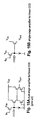
- This lateral diffusion effect which is a problem in previous designs, is actually a phenomenon on which the present invention relies for efficacy. According to a specific embodiment of the invention and as shown in Fig.
- stimulating light 108 e.g., red light
- stimulating light 108 may be delivered in the form of a single LED or a laser pencil beam (e.g., for a pixel-by-pixel readout), or an array of LEDs or a laser fan beam (e.g., for a line-by-line readout).
- the region directly exposed to stimulating light 108 and the imaging area are adjacent linear regions on the surface of plate 102 and detector 114 comprises a linear array of photodetectors.
- the linear array of photodetectors may be in contact or very close proximity with the plate with the stimulating light source exposing the area of the plate adjacent to photodetectors.
- the linear array of photodetectors and the stimulating light source are transported simultaneously across the plate with the linear array of photodetectors leading and the stimulating light source trailing.
- the area of the plate under the linear array of photodetectors is read because of the diffused stimulating light, and then, according to specific embodiments, is fully erased by the trailing stimulating light.
- the approach of the present invention runs counter to previous techniques which generally try to avoid stimulating an area outside the imaging area for fear of not collecting all the stimulated light and losing information.
- the imaging area becomes indirectly stimulated by light 116 laterally diffused within the plate rather than by direct exposure to stimulating light 108.
- reliance on the lateral diffusion of stimulating light within the plate allows stimulation of an area of the plate from the side rather than from the bottom or from the top.
- This allows elimination (or minimization) of any gap between the plate and detector 114 which would otherwise be necessary for the stimulating light to impinge on the plate in the same area as the imaging area.
- Indirect stimulation of a desired region of the plate in this manner allows for the detector(s) to be placed in direct contact with (or in very close proximity to) the imaging region, thus resulting in high collection efficiency as well as high spatial resolution.
- this design does not require a special transparent plate. Rather, it can be implemented using conventional turbid storage-phosphor plates. This is a significant benefit in that transparent plates are expensive and very difficult to manufacture whereas conventional plates are easy to manufacture and readily available.
- Another benefit of the design of the present invention is that the stimulating hardware and collecting hardware may be disposed on the same side of the plate. According to such embodiments, the overall profile of the hardware can be made very low. According to one such embodiment (described below), the hardware is configured so as to fit into an enclosure with dimensions substantially similar to those of a standard film cassette. As will be understood, such an embodiment would be problematic (and likely impracticable) using stimulating hardware and collecting hardware on opposite sides of the plate.
- Yet another benefit associated with placement of the stimulating hardware and collecting hardware on the same side of the storage-phosphor plate relates to the alignment and registration of the stimulating hardware with the collecting hardware. According to a specific embodiment which will be described with reference to Fig. 2 , a self-aligned assembly of the stimulating and collecting hardware is provided.
- Fig. 2 shows a self-aligned arrangement for the stimulating light. That is, the linear array of photodetectors blocks the stimulating light from the plate. The edge of the linear array defines the boundary between the area of the plate directly exposed to the stimulating light and the area of the plate indirectly exposed to stimulating light through diffusion. More specifically, a linear array 202 has a photosensitive area 204 which extends to the edge of its substrate. The area of plate 206 adjacent that edge is exposed to stimulating light 208 to achieve a perfectly aligned and well-controlled stimulation area under linear array 202.
- linear array 202 acts as a knife edge for stimulating light 208, forming a self-aligned mask which allows surface exposure only to a linear region adjacent photosensitive area 204 of array 202.
- the width of the stimulated area under photosensitive area 204 relates to the intensity of stimulating light 208 in the exposed region of the plate as well as the attenuation coefficient in the plate itself.
- the intensity of the laterally diffused stimulating light decreases exponentially moving away from the edge of an exposed region in a well defined manner.
- the stimulating light intensity and/or the linear array photosite may be varied in accordance with particular applications of the present invention.
- a significant advantage associated with the self-aligned nature of such an embodiment of the invention is the fact that careful focusing of the stimulating light using, for example, a laser fan beam, is not necessary.
- the applied light can be relatively diffuse as delivered, for example, with an inexpensive array of LEDs.
- Figs. 1 and 2 illustrate some of the basic principles of the present invention. However, it will be understood that in some cases it will not be practical to position a linear array of photodetectors in contact with a phosphor plate. That is, the photosensitive side of the linear array often includes the bonding area for the interconnecting wires. These wires typically protrude above the photosensitive surface and prevent any other surface from being placed against it. These wires are also very small and fragile and must be protected from any direct contact with a moving surface. The photosensitive surface of the linear array itself is also fragile and needs to be protected from direct contact with a moving surface.
- One method for protecting both the wire bonds and the photosensitive surface involves the use of a fiber-optic faceplate between the photosensitive surface of the linear array and the phosphor plate.
- the fiber-optic faceplate may be permanently bonded to the photosensitive side of the linear array, thus clearing the wire bonds from the phosphor plate.
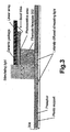
- Fig. 3 illustrates such an specific embodiment in which collection of stimulated light in response to laterally diffused stimulating light is effected through a fiber-optic face plate 302. It should be noted that the gap between the surface of storage medium 304 and fiber-optic face plate 302 has been exaggerated for illustrative purposes.
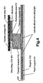
- Fig. 4 shows a further refinement of the arrangement shown in Fig. 3 .
- the edge of the fiber-optic faceplate creates the boundary between the directly exposed area of the plate and the indirectly exposed area of the plate. The sharpness of this edge is important to the uniformity of the diffused light profile under the detector array.
- two fiber-optic faceplates against each other (one for illumination with stimulating light, one for collection of stimulated light) it is possible to protect the edge of the collecting faceplate against chipping and cracking of the edge of the collecting faceplate.
- a single apparatus is provided to effect both the stimulating and collecting functions.
- this configuration facilitates simultaneous scanning of the stimulating and collecting apparatus as well as provides a low profile for packaging of the readout apparatus with the storage medium in, for example, a standard radiography cassette.
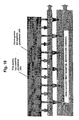
- the linear array of detectors 404 are combined in ceramic package 406 with a two dimensional array of LEDs 408 which provide the stimulating light to storage-phosphor plate 410 which comprises a storage phosphor layer 412 on a plastic substrate 414.
- the stimulating light from LEDs 408 is transmitted to the surface of the phosphor 412 via a first fiber-optic faceplate 416.
- faceplate 416 may comprise a block of uniform material such as glass or plastic as transmission of the stimulating light to the surface of phosphor 412 via fibers is not critical to the operation of the invention.
- the stimulating light diffuses in phosphor 412 into the region below the photosensitive regions 418 of detectors 404.
- This indirect stimulation of this region of phosphor 412 results in the release of previously stored information as stimulated light which is then captured by detectors 404 via a second fiber-optic faceplate 420.
- the source of the stimulating light and the means by which the subsequently released energy is captured are disposed in the same package, alignment of these two elements is consistent and reliable.
- the simultaneous and coordinated scanning of the arrays of LEDs and detectors across the surface of the storage-phosphor plate can be managed with a single mechanism such as, for example, a precision stepper motor.
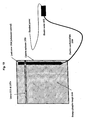
- Fig. 5 shows a system 500 for capturing and reading out image data for use with, for example, radiography systems.
- storage medium 502 e.g., a storage-phosphor plate
- the release and capture of the stored information may be effected by scanning a linear readout apparatus 504 designed according to the present invention across the surface of storage medium 502.
- readout apparatus may comprise a single apparatus such as that described above with reference to Fig. 4 in which both the source of stimulating light and the detector array are included.
- apparatus 504 may comprise two separate apparatus the operation and scanning of which are closely coordinated to effect readout in the manner described herein.
- readout of information in storage medium 502 is effected by indirect stimulation of the region of interest according to the techniques described above. Movement of apparatus 504 may be controlled via scanning control 506 which generates signals to control a mechanical actuator 508 which may include, for example, a precision stepper motor. As will be understood, any of a variety of techniques may be employed to effect the precise, e.g., line-by-line, scanning of readout apparatus 504 over storage medium 502.
- Stimulated light is released from storage medium 502 and captured by the detectors of readout apparatus 504 as controlled by readout control 510 according to any of a variety of well know techniques which convert captured radiation to electrical or optical data which may then be stored for later retrieval. It will be understood that scanning control and readout control via 506 and 510 may effected in a variety of ways without departing from the scope of the present invention. For example, such control may be effected using microprocessor controlled circuitry, application specific integrated circuits, or software.
- Fig. 6 illustrates yet another specific embodiment of the present invention in which a readout apparatus and storage medium combination such as that described above with reference to Fig. 5 may be integrated in a cassette 602 which may be a standard size for a particular application, e.g., a radiography cassette.
- Control of the readout mechanism 604 and readout of data from storage medium 605 could be effected via connector (not shown) which may comprise any of a variety of commercially available parallel or serial connectors.
- readout of data could be effected via one or more conductors exiting cassette 602.
- such a device could be conveniently used with the existing installed base of radiography systems. That is, the standard size cassettes could be inserted into an existing radiography table for capture of x-ray images in the same manner as the standard film cassettes.
- the image data may then be read through suitable connections, e.g., a connector or bundle of conductors, while the cassette conveniently remains installed in the radiography table, i.e., in-situ readout.
- the cassette may be removed and connected to a reader (which may be a conventional PC or work station). Readout (and simultaneous erasure) of the stored information is then effected in the manner described above, after which the cassette is ready for subsequent image capture.
- the present invention includes implementations integrated into any standard size radiography cassettes as defined by international standard IEC 60406.
- cassette dimensions include, but are not limited to, 14" x 17", 14" x 14", 10" x 12", 8" x 10", 35 cm x 43 cm, 35 cm x 35 cm, 20 cm x 40 cm, 18 cm x 43 cm, 13 cm x 18 cm, 13 cm x 30 cm, 18 cm x 24 cm, and 24 cm x 30 cm.
- a line-by-line scanning of a standard 14"x17" image could be effected using the techniques of the present invention in roughly 10 seconds which compares favorably to the several minutes required for development of conventional film.
- the image is electronically stored and can be permanently archived for later retrieval without having to physically store the large developed image.
- cassette 602 may vary without departing from the scope of the present invention.
- the readout apparatus and mechanical scanning mechanism can take a variety of forms.
- various parts of the scanning and readout control may be integrated with cassette 602.
- one or more microprocessors and associated control circuitry may be included in cassette 602 to effect scanning and image capture as instructed by control signals from an external computer. Scanning and image capture could even be effected entirely within the cassette which could include sufficient onboard memory for temporarily storing the image until it can be downloaded for viewing and archiving.
- control signals for scanning and image capture may be effected entirely outside of the cassette with data being transmitted back and forth via, for example, a connector.
- the present invention contemplates and encompasses any of a variety of combinations of on and offboard control of the scanning and data capture functions.
- the fundamental principle of the present invention is the stimulation of an area of a storage plate through lateral diffusion of the stimulating light within the plate.
- a number of optimizations may be made for each of the components of such a system.
- some of these optimizations are independent of this fundamental principle, and as such constitute independent inventions.
- Various components of such systems are discussed herein and include storage plates, fiber-optic faceplates, sources of stimulating light, linear arrays of photodetectors, filters for blocking stimulating light, scanning mechanisms and system housings.
- the physical parameters of the storage plate employed for the present invention may be correspondingly different. That is, the thickness of the plate, the grain size of the phosphor, the amount of binder, and the amount of dye may be altered from that which is appropriate for conventional techniques for improved performance of the techniques of the present invention.
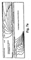
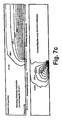
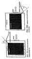
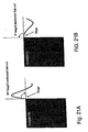
- the amount of energy-absorbing dye (i.e., dye which absorbs electromagnetic energy at the wavelength of the stimulating light, e.g., red light) in the storage plate can be manipulated to control the amount and profile of the lateral diffusion of the stimulating light as shown in Figs. 7a-7c .
- Each pair of graphs in Figs. 7a-7c shows the absorption profile of the red stimulating light (top graph) and the point spread function of the resulting blue stimulated light (bottom graph) for different concentrations of red-absorbing dye in the plate as simulated using the Monte Carlo simulation technique.
- Each gradation in the respective graphs represents a 10% increment.
- Figs. 7a-7c indicate that it is now possible, with the techniques described herein, to indirectly stimulate the plate with the same energy level across its entire depth. These graphs illustrate the fact that, as the stimulating light diffuses further and further away from the exposed edge, its energy distribution becomes homogeneous across the entire thickness of the plate. This phenomenon can be used to create an x-ray imaging system with very high resolution and yet very good x-ray absorption.
- the resolution is limited by the lateral diffusion of the stimulating light as well as the stimulated light.
- the resolution is only limited by the lateral diffusion of the stimulating light (which can be controlled by the amount of red-absorbing dye) and not by the lateral diffusion of the stimulated light.
- the photodetectors aperture (along the direction of the mechanical scanning) does not impact the resolution but simply the collection efficiency. Even with a 200 ⁇ m photodetector aperture, it is possible to achieve much finer resolution (as low as 20 ⁇ m).
- the resolution of a turbid storage-phosphor plate in the direction of mechanical scanning can be as high as the resolution of a needle phosphor plate. This is true even when a thick storage-phosphor plate (i.e. 300 ⁇ m) is used to capture high energy x-rays.
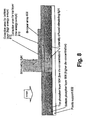
- top layer 804 contains a small amount of dye which is meant to absorb weakly the stimulating light
- bottom layer 806 contains a higher amount of dye which is meant to absorb strongly the stimulating light.
- the top layer 804 is stimulated further away from the edge of the direct stimulating light exposure than the bottom layer 806.
- stimulated light from the top layer is collected in the first row of photodetectors 810 whereas stimulated light from the bottom layer is collected in the second row of photodetectors 812.
- the top layer 804 absorbs low energy x-rays whereas the bottom layer 806 absorbs higher energy x-rays.
- soft material such as human soft tissue
- dense material such as human bone
- information collected from the top and bottom layers is used to create a dual-energy image. Dual energy data may then be processed to extract information corresponding to bone or soft tissue only.
- images may be created which display bones only or soft tissue only.
- a variety of embodiments are envisioned using multiple layers of various storage-phosphor materials and multiple rows of photodetectors to achieve dual-energy imaging.
- phosphor plates are manufactured on a flexible substrate (PET, Mylar) like prompt phosphor screens. These plates are either mounted on a hard backing (e.g., an aluminum plate) or are kept flexible in order to be transported and read in the laser scanning apparatus. Therefore, according to a specific embodiment of the present invention, in order to maintain sufficient contact between the surface of such a flexible phosphor plate and the light collection apparatus, e.g., a fiber-optic face plate, the phosphor plate is mounted on a thin foam layer which is compressed when the light collection apparatus is pressed against the surface of the plate. According to a more specific embodiment, where the light collection apparatus is held at each side, the foam can be make thicker at the center of the plate than at the edge to ensure sufficient contact across the entire width of the plate (e.g., see Fig. 9 ).
- the fiber-optic faceplate of the present invention may serve two purposes, i.e., creation of a knife-edge alignment for the stimulating light, and collection of the stimulated light onto the photo detectors.
- the edge of the faceplate defines the illumination boundary and its sharpness is important for achieving optimal performance.
- another such faceplate can be mounted against it (e.g., plate 416 of Fig. 4 ) or, alternatively, a clear block of transparent material (e.g., glass or plastic) can be mounted against it. The choice of material will depend on the amount of collimation required for the stimulating light.
- a clear material can be used. If additional collimation is required, another fiber-optic faceplate can be used to transport the stimulating light onto the plate. As will be understood, the amount of additional collimation is determined by the numerical aperture of the fiber-optic faceplate. If a low numerical aperture is chosen, the stimulating light hitting the plate will be highly collimated. Regardless of the nature of the block mounted against the collection face plate, the edge of the collection faceplate is protected against chipping or other damage during operation.
- the fiber-optic faceplate may be cut at a slight angle with respect to the direction of the fibers as shown in Fig. 4 .
- Such a slight bias cut may allow for an easier alignment of the faceplate onto the linear array without reducing significantly its transmission characteristics, e.g., a bias cut angle of less than 10 degrees will result in a 10% transmission reduction.
- the collection fiber-optic faceplate may also serve another important purpose. That is, it can be configured to block partially or completely the stimulating light.
- the fiber-optic faceplate may be constructed from materials which absorb the stimulating light and transmit the stimulated light.
- Such materials may include optical filter materials such as ionically colored glass e.g. Schott BG3.
- optical filter materials such as ionically colored glass e.g. Schott BG3.
- rare earth doped filter glasses are better candidates for fiber-optic faceplates.
- rare earth doped filter glasses may also be used as a filter material.
- Thulium doped glass has good transmission characteristics at 400 nm and good absorption characteristics at 680 nm. Therefore, according to a specific embodiment of the invention, a low index host glass and a high index host glass are doped with Thulium to create a cladding and a core material. These core and cladding materials are then bundled together to create fiber-optic faceplates for use with the present invention having good transmission characteristics (i.e., high numerical aperture) and good rejection of stimulating light.
- the transmission of a fiber-optic faceplate is a function of the numeral aperture of each fiber.
- the numerical aperture of each fiber increases as the difference in refractive indexes between the core and cladding increases.
- Fiber optic faceplates are traditionally manufactured from glass since high index and low index materials are easily available. This has not been the case for plastic materials, i.e., most of them tend to have a refractive index close to 1.4.
- a new plastic material is now commercially available from the Florida-based company Optical Polymer Research Inc. Until recently, most fiber-optic faceplates have been manufactured from glass since materials having a sufficient index differential are easily available. Recently, a new class of plastic material has been developed.
- This new material marketed under the name Opti-Clad, has a very low refractive index (less than 1.36) and as such is suitable for use as a cladding material around, for example, a styrene core (refractive index close to 1.59). Teflon is also another good cladding material since its refractive index is 1.3.
- an energy-absorbing dye is introduced into the plastic employed to make such a fiber-optic faceplate to obtain a faceplate with a high numerical aperture and good rejection of stimulating light.
- Another approach to blocking the stimulating light involves the use of a reflective (rather than refractive) cladding material in the fibers of the fiber-optic faceplate.
- a reflective (rather than refractive) cladding material in the fibers of the fiber-optic faceplate.
- Such fibers are not ideal for transmission of light energy over long distances due to the loss of energy at each reflection.
- such fibers will be sufficiently transmissive.
- the fiber optic faceplate may be useful for creating a knife-edge for the stimulating light, for collecting and imaging the stimulated light onto the photodetectors, and additionally for preventing the stimulating light from reaching the photodetectors. It is possible however to implement the present invention without using a fiber optic faceplate (as shown in figures 1 and 2 ).
- a beveled transparent layer is employed which is thin above the photosensitive area of the linear array and thick above the bonding area of the linear array. This implies that the linear array is not positioned parallel to the image plate. As shown in Fig. 10b , the linear array 1002 is placed at an angle with respect to the plate 1004 so as to bring the photosensitive area 1006 closer to the plate and the bonding area further away from the plate. Using this technique, one can minimize the thickness of the transparent layer 1008 over the photosensitive area and maximize it over the bonding area.
- the linear array is placed in a cavity and a liquid transparent epoxy is poured over it.
- a liquid transparent epoxy is poured over it.
- the epoxy Once the epoxy has cured, it creates a hard transparent layer which is thin over the photosensitive area and thick over the bonding area of the linear array.
- the bond wires can be directly encapsulated by the epoxy or can be first coated with a resilient material (e.g., silicone) before they are covered with the epoxy so as to alleviate issues related to mismatch in coefficients of thermal expansion.
- a resilient material e.g., silicone
- the mold can be as simple as a perfectly flat Teflon-coated surface placed in front of the linear array which will hold the epoxy while it is poured and which will be removed after the epoxy has cured.
- a one-part epoxy such as 4021T manufactured by Ablestick is employed. This epoxy will adhere to glass and silicon but will not stick to the Teflon-coated surface.
- the transparent epoxy can also contain the absorbing dye necessary to block out the stimulating light (as it is described further on in this document).
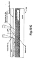
- a second technique illustrated in Fig. 10a comprises using a transparent layer 1022 made of a high index material (n ⁇ 1.6). Light emitted from the plate 1024 will be refracted in the high index material 1022 at a smaller angle with respect to the normal incidence (Snell law). The resulting blurring will thus be reduced.
- a third technique illustrated in Fig. 10c comprises depositing an interference filter 1042 on the surface of the transparent layer 1044 in contact with the image plate 1046.
- the purpose of the interference filter is to transmit the stimulated light emitted by the plate that reaches the filter at angles close to normal incidence, and to reflect back to the plate the stimulated light that reaches the filter beyond a certain angle.
- This type of interference filter is used in front of prompt-emitting phosphors in order to create a forward-peaking distribution, that is to increase the intensity of the light emission in the forward direction and to decrease it in the off-axis directions.
- This technique is particularly useful for maximizing the optical coupling between a CRT phosphor screen and a projection lens (e.g., in a large-screen TV), or between a prompt emitting phosphor and a lens-based camera ( Norikata Satoh, SPIE volume 2432 page 462-469 ).
- This technique increases the intensity of the light emitted in the forward direction at the expense of the spatial resolution.
- This technique is used in this invention not for the purpose of collecting more light but for the purpose of rejecting off-axis light that contributes greatly to the blurring effect.
- this material should not scratch the image plate. Removing dust and dirt from the contact area will reduce chances of scratches.
- an additional layer of Teflon-like material is coated on the plate or the material itself to reduce friction between the two surfaces.
- the outer edges of the surface in contact with the image plate are beveled or rounded to reduce the chances of scratches.
- the source of stimulating light comprises a row of light emitting diodes (LEDs) mounted close each other.
- LEDs light emitting diodes
- Such arrays of LEDs are available commercially, e.g., StockerYale linelights. Examples of such modules include 100 LED chips mounted directly on 100mm substrate with a spacing between each LED of 1 mm.
- the overall illumination of a typical LED array is fairly uniform across the length of the array.
- One of the advantages of the method of light stimulation proposed in the present invention is that it can be made relatively insensitive to variations of illumination across the length of the array by ensuring that the amount of illumination is sufficiently high to bleach the entire depth of the plate. According to one embodiment, reaching this threshold is ensured by including one or more additional rows of LEDs next to the first row in order to increase the amount of stimulating light in the plate.
- the LEDs' peak emission wavelength matches the peak absorption wavelength of the filter which is placed between the plate and the photodetectors.
- the LEDs are chosen to have an emission spectrum range which is narrower than the effective absorption range of the filter.
- an additional filter is added between the LEDs and the plate. The purpose of this additional filter is to block any wavelength of stimulating light which would not be blocked by the primary filter between the plate and the photodetectors.
- control circuitry is provided to adjust the brightness of the LEDs. The control circuitry can be used to reduce the brightness of the LEDs in order to achieve partial bleaching of the plate.
- additional rows of different color LEDs are provided to achieve greater erasing efficiency. It has been demonstrated that storage-phosphor plates are more efficiently erased under broadband illumination than monochromatic illumination. Therefore, adding rows of ultra-violet, blue, green, yellow, orange or infrared LEDs to the rows of red LEDs is proposed to simulate broadband illumination and increase the erasing efficiency.
- a specific embodiment of the present invention introduces a novel way to implement a two-stage erasure method. Fluorescent tubes are replaced with rows of LEDs. A first erasure stage is constructed using UV LEDs only. UV LEDs are now commercially available from a number of manufacturers (e.g. Nichia NSHU-550E or NSHU-590E). These LEDs put out approximately 1mW between 370nm and 375nm. They also produce a very low visible output (dim purple glow) which can be easily filtered out. A second erasure stage is constructed using various other color LEDs which did not produce any UV light.
- the linear array of photodetectors for use with the present invention can be built in a variety of different ways.
- discrete photodetectors can be mounted in a single row and connected to a multiplexing circuitry.
- an amorphous silicon array of photodetectors can be used.
- photodetectors built on a single crystal silicon substrate are preferred.
- Such linear arrays can be manufactured using charge-coupled device (CCD) or CMOS technology.
- CCD charge-coupled device
- CMOS technology for image sensors has improved tremendously in the last few years and the performance characteristics of CMOS image sensors are approaching those of CCDs. It should be understood that the present invention does not exclude any of the available photodetection technologies.
- various embodiments of the present invention provide further enhancements which will now be described.
- the present invention provides antireflection coatings for linear CCD arrays to reduce the amount of reflection off the silicon surface.
- Multi-layer coatings e.g., Haffnium oxide
- Multi-layer coatings can be used to increase the quantum efficiency of front-illuminated linear CCDs from 60% to 95% at 400 nm (e.g., the wavelength of stimulated light).
- such multi-layer coatings can also be used to decrease the quantum efficiency of front-illuminated linear CCDs from 80% to 1% by reflecting light at 650 nm (e.g., the wavelength of stimulating light). That is, these multi-layer coatings can be implemented to act as a blocking filter for the stimulating light and an antireflective layer for the stimulated light.
- linear CCDs rely on photodiodes or junction gates as a photodetectors.
- additional process steps are taken which increase the cost and complexity of the CCD manufacturing process.
- An easier and cheaper process could be used to manufacture linear CCDs, such as the one used for full-frame area CCDs, but it would be at the expense of the blue quantum efficiency.
- Full-frame area CCDs use a simple manufacturing process in which the vertical registers act as photodetectors. They exhibit a low quantum efficiency in the blue region of the spectrum ( ⁇ 10%) because the vertical registers are covered with polysilicon gates which absorb strongly at these wavelengths. Attempts have been made to increase the blue quantum efficiency by thinning the polysilicon gates or removing such gates over parts of the photodetector area.
- a technique is introduced to increase the blue quantum efficiency of linear CCDs manufactured using a conventional full-frame area CCD process.
- the proposed photodetector layout includes a narrow polysilicon gate (i.e., a photogate) surrounded on both sides by wide channel stop regions (which are not covered by polysilicon gates).
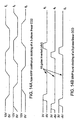
- This photodetector design is dramatically different from conventional linear CCD photodetectors since the channel stop region between the photodetectors is much wider than the photodetector itself (see the comparison in Figs. 11a and 11b ).
- narrow channel stop regions 1102 are implanted between photodetectors 1104 to form a sharp potential barrier between them ( Fig. 11a ).
- the channel stop region exhibits high quantum efficiency but no strong electric field, so electrons generated in that region can laterally diffuse on either sides to the two adjacent photodetectors.
- the channel stop width is kept to a minimum to create the sharpest separation possible between photodetectors, thus increasing the contrast (i.e., MTF).
- the photodetector response can be represented by a trapezoid-shaped curve, which approaches the shape of a rectangle if the channel stops are narrow compared to the photodetector width ( figure 12a ).
- channel stops 1152 are wider than the photodetectors 1154 ( Fig. 11b ), which creates a triangular-shaped photodetector response curve ( figure 12b ). As can be seen from the figure, this reduces the isolation between adjacent photodetectors (i.e., creates a more overlapping response). According to a more specific embodiments, this effect is mitigated by providing photodetectors on a finer pitch than the required resolution and combining their signals at the output of the CCD register (analog binning technique) or after they have been digitized ( figure 12c ). This design achieves the original goal of increasing the blue quantum efficiency and also helps decrease the dark current generation in the photodetector since channel stop regions generate less dark current than CCD channels.
- an area CCD is used to emulate a linear CCD, i.e., signals from the photodetectors of the same column of an area CCD are combined in the horizontal output register to form a single large-aperture photodetector.
- signals from the photodetectors of the same column of an area CCD are combined in the horizontal output register to form a single large-aperture photodetector.
- five 44 ⁇ m x 44 ⁇ m photodetectors may be binned to emulate a 220 ⁇ m x 44 ⁇ m photodetector.
- the proposed area CCD resembles a Time Delay Integration (TDI) CCD in its aspect ratio (5 x 2,048 pixels), but it is not used in a TDI mode. This design alleviates the serious problem of readout lag encountered with large-aperture photodetectors.
- TDI Time Delay Integration
- photodetectors with an aperture greater than 100 ⁇ m exhibit significant readout lag as reported in the data sheets of linear CCDs designed for barcode readers (e.g., Toshiba TCD1304AP, Sony ILX511). This is due to the fact that the electric field in the photodetector region is not strong enough to move small charge packets across a 100 ⁇ m distance into the output register.
- the gate length can be kept under 15 ⁇ m. Since no spatial resolution is required along the columns of the area CCD, larger gates can be used with no implant barriers between them.
- An example of such a design is illustrated in Fig. 13 .
- Five 44 ⁇ m photogates 1302 are laid out vertically along the CCD buried channel. As shown in the associated timing diagram, the photogates are biased negatively during the integration time (MPP mode described below) and clocked briefly in a ripple fashion to transfer the charge packets into the output register.
- the device In this mode of operation, the device is truly a linear CCD since it cannot image in the vertical direction. Even though the device layout resembles one of an area CCD, the photogates can only ripple the charge into the output register but cannot isolate separate charge packets since they are all tied to the same voltage. As described in a previous embodiment (dual-layer plate for dual-energy imaging), it may be necessary to collect information from two adjacent rows of photodetectors instead of one. It is possible to operate the same linear device shown in Fig. 8 as a bilinear device (two adjacent rows of photodetectors) by simply changing the photogates timing.
- V PG3 acts as a barrier between a first photodetector (consisting of V PG1 and V PG2 ) and a second photodetector (consisting of V PG4 and V PG5 ).
- first photodetector consististing of V PG1 and V PG2
- second photodetector consististing of V PG4 and V PG5 .
- a specific embodiment of the present invention provides a method for reducing the dark signal of the linear CCD.
- This method is inspired from the technology known as MPP, which was developed for areas CCDs only.
- MPP Magnetic Pinned Phase
- the MPP technology significantly reduces the dark current generated in the vertical registers of area CCDs. This is accomplished by introducing a weak implant under one gate and by biasing all the gates negatively (total inversion) to pin the Si-SiO 2 interface to the substrate voltage (MPP: Multi-Pinned Phase). Further details can be found in the book entitled “Solid-state imaging with charge-coupled devices", A. Theu ceremonies, on page 289.
- the gates of such devices are usually clocked constantly and do not get pinned to a low voltage for any significant length of time (i.e., the high duty cycle of Fig. 14a ). Under those conditions, the MPP operation would not be effective at all and this is why it has not been implemented on any commercial devices.
- the MPP mode is implemented in the output register of a CCD by introducing an MPP barrier implant under one gate and by clocking all the gates in a burst mode instead of a continuous mode ( Fig. 14b ).
- Modifying the timing diagram of the register from continuous mode to burst mode changes the duty cycle from a high duty cycle to a low duty cycle. This allows for all the gates to be pinned to a low voltage for a significant length of time, thereby making the MPP mode effective for such devices.
- the MPP mode is implemented in four-phase CCD output register by introducing an MPP barrier implant under two gates (instead of one) of the four phases.
- the MPP barrier implant is under the gates ⁇ H2 and ⁇ H4 but not under the gates ⁇ H1 and ⁇ H3 .
- This design allows for great flexibility in the operation of the output register.
- the output register can be operated in a conventional four-phase clocking mode (as shown in Fig. 18 ).
- the output register can also be operated in a two-phase clocking mode by connecting two adjacent gates.
- Linear CCDs have been designed historically for industrial and document scanning applications and, as a result, have not benefited from some of the technology advances made with regard to scientific area CCDs.
- linear CCDs feature high-speed readout amplifiers (e.g., the two-stage FET amp shown in Fig. 15a ) but not low-speed, low-noise readout amplifiers. Therefore, the present invention provides a linear CCD for use with various embodiments using a low-speed low-noise amplifier (e.g., a single-stage FET amp) ( Fig. 15b ).
- the purpose of this design is to achieve a readout noise close to 10 electrons at 500 kHz as compared to the readout noise of a conventional linear CCD which is close to 300 electrons at 5 MHz.
- a technique in which the binning of the photodetector signals at the output of the CCD register is dynamically controlled.
- Analog binning techniques have been used in the past to change the effective photodetector area and overall resolution of CCDs.
- the binning process is controlled "on the fly” to increase the dynamic range of the system as opposed to modifying its resolution.
- a linear CCD with four times as many photodetectors as required is used.
- the signals from four adjacent photodetectors are combined systematically as they reach the output of the register, regardless of their signal value.
- combining four signals can result in saturation of the readout circuitry (i.e., an undesirable dynamic range limitation).
- the signal of only one photodetector is read out and compared to a threshold before deciding if it will be combined with the signals of its three neighboring photodetectors. If the signal value is below a certain threshold, the signals of the following three photodetectors are binned with the signal just measured, and the combined signal is re-measured.
- additional binning e.g. combining signals from eight adjacent photodetectors instead of four
- additional binning is effected in order to further increase the sensitivity of the system, and thus the dynamic range.
- dynamically-controlled binning refers to the fact that binning only occurs for certain signal values and the decision process is performed "on the fly”. This technique works particularly well in this application because the signal values of neighboring photodetectors are close to each other. This is due to the fact that the photodetectors are small ( ⁇ 20 ⁇ m ) compared to the point spread function of the storage-phosphor plate ( ⁇ 120 ⁇ m).
- a bilinear CCD is provided (see Fig. 16 ) in which one shift register collects charges from wide pixels 1602 (high sensitivity) and the other register collects charges from narrow pixels 1604 (low sensitivity) interlaced with the wide ones.
- a single shift register linear CCD is provided (see Fig. 17 ) in which odd pixels 1702 are narrow and even pixels 1704 are wide.
- the narrow pixels are read first and compared to a pre-determined threshold. If the pixel value is above the threshold, the pixel value is validated and the associated wide pixel is discarded (i.e., it contains no information since it is saturated). If the pixel value is below the threshold, the output amplifier is not reset, the associated wide pixel is binned with the narrow pixel, and a combined value is measured and validated. For low signal levels, no information is discarded and all the charges are read. For high signal levels, only a small fraction of the signal is read (ratio between the widths of narrow and wide pixels) but this process does not introduce any additional noise. This readout process can result in significant increases in the dynamic range of the device corresponding roughly to the ratio of the alternating pixel sizes.
- Similar binning techniques can be used with different pixel architectures as well as in the cross-scan direction. That is, the pixel value information along each line can be dynamically compared to a pre-determined threshold to determine which mechanical scanning pitch is appropriate. If the signal levels are very low, a larger sampling pitch can be used to maximize the sensitivity. If, on the other hand, the signal levels are high, a smaller sampling pitch can be used to maximize the spatial resolution.
- This dynamic resolution/sensitivity optimization can be implemented along the scanning direction as well as the cross-scanning direction. It should be noted that these dynamic range extension techniques are particularly important where the dynamic range of the CCD output amplifier has been intentionally reduced to maximize its sensitivity.
- the photosensitive area is kept as close as possible to the long edge of the chip since this edge defines the boundary of the illumination area and therefore the area where the stimulated light is generated.
- Conventional linear CCDs have been designed for industrial and document scanning applications and therefore have their photosensitive area placed in the center of the chip (typically 1mm to 2 mm away from the edge).
- the techniques developed for scientific buttable area CCDs are utilized to manufacture a linear CCD which has minimal dead space between its photosensitive area and three edges of the chip (e.g., typically less than 50 ⁇ m).
- the minimal dead space along the long edge facilitates maximum light collection.
- the minimal dead space at each extremity of the linear array allowing the abutting of multiple arrays to create an uninterrupted photosensitive area.
- the maximum length of a linear CCD array is determined by the size of the wafer on which it is manufactured. Typically 5" or 6" wafers are used to manufacture CCDs. This sets the practical limit for the length of the linear CCD below 4".
- 4 mechanically-butted CCDs are employed, each featuring a single row of 2048 pixels on a 44 ⁇ m pixel pitch.
- Each CCD is 9cm long by 0.2cm wide.
- a special coating may be applied to the photodetectors to bring the frontside quantum efficiency up to, for example, 95% at 390 nm.
- Each CCD features two very low noise single-stage amplifiers (8 e - @ 30°C & 400kHz).
- the shift register well capacity is sized for optimal dynamic range and room temperature dark signal.
- the CCD pixels may also be sized for optimal dynamic range and room temperature dark signal (for example 9 ⁇ m wide odd pixels and 81 ⁇ m wide even pixels).
- Another specific embodiment for a linear CCD is presented in Fig. 18 .
- multi-layer interference filters may be deposited on either or both sides of the fiber-optic faceplate.
- an energy-absorbing material which absorbs electromagnetic energy at the wavelength of the stimulating light (e.g., red light) is added to the optical cement which is used to bond the fiber-optic faceplate to the linear array, or in the optical epoxy which is used as a transparent layer between the plate and linear array.
- a typical glue line thickness between the fiber-optic faceplate and the linear array is 20 ⁇ m. If the glue line thickness is much thicker than 50 ⁇ m, a loss of spatial resolution may occur.
- Certain dye materials can be manufactured with extremely high absorption characteristics (e.g. cyanines). Therefore, according to specific embodiments, such dyes are mixed in epoxy materials in high concentration so as to absorb all the stimulating light within a very thin layer (e.g., less than 20 ⁇ m).
- a very thin layer e.g., less than 20 ⁇ m.
- One example of such a dye is a product manufactured by American Dye Source, Inc. (Quebec, Canada) referenced ADS 640HI and with the chemical formula C 39 H 55 N 2 I. Its extinction coefficient is 200,000 l/mol/cm at 643 nm. Its solubility is roughly 0.05 mol/l. For a 10 ⁇ m thickness (0.001 cm), the transmission at 643 nm is therefore 10 -10 , which is sufficiently low to guarantee that no stimulating light will reach the photodetectors
- the chemical composition of the dye is changed to quench its natural fluorescence. Quenching the fluorescence of laser dyes in the red region of the spectrum has not previously been achieved. Other techniques have been used to circumvent this problem.
- European patent application EP 1 065 525 A2 describes a method for filtering out the fluorescence of the laser dye by combining it with a conventional colored glass filter (e.g. 1mm Schott BG39).
- the conventional colored glass filter does block the fluorescence of the laser dye but introduces an unacceptable additional thickness in the optical path. It is desirable to eliminate the fluorescence without introducing an additional filter layer.
- the chemical composition of the laser dye is modified to stop it from fluorescing.
- This goes against traditional approaches which have been aimed at maximizing (rather than minimizing) the fluorescence of laser dyes in order to increase the laser efficiency.
- This embodiment is based on the fact that certain infrared dyes do not fluoresce, such as the dye ADS812MI manufactured by American Dye Source.
- ADS812MI has a peak absorption at 812 nm and the following chemical formula: C 40 H 40 Cl N 2 I. It appears that the presence of chlorine in the molecule may relate to the fact that this dye does not fluoresce. Therefore, according to this embodiment of the invention, chlorine is introduced into the chemical composition of the red dye (as a form of perchlorate for example) to inhibit its natural fluorescence.
- One scanning mechanism for use with the present invention is a bi-directional translation stage on which the linear photodetector array and the row of illuminating LEDs are permanently mounted.
- the forward scanning direction of the stage is used to read and erase the plate simultaneously, whereas the reverse scanning direction of the stage may be used for additional erasing of the plate (if necessary) in addition to bringing the stage back to its starting position. Due to the asymmetrical stimulation of the plate (knife edge illumination), the reading of the plate can only occur in the forward scanning direction.
- various mechanisms may be employed to translate the stage across the plate including, for example, a motorized lead screw, a motorized belt, a magnetic linear motor, and an inchworm motor.
- stage translation solutions allow for the outer dimension of the stage and scanning mechanism to remain below half an inch (1/2") in thickness. This dimension is important for the embodiments of the invention intended to fit inside a cassette the size of a conventional film cassette as described above with reference to Fig. 6 . Such an accomplishment is particularly impressive when compared to current laser scanning reading apparatus which are roughly the size of a household refrigerator.
- the motor (which drives the lead screw or the belt) can be fitted inside or outside the film-like cassette.
- a small electric motor e.g., Mabuchi motor reference FF-N30VA
- Such low-profile electric motors are commonly available since they are used in numerous consumer electronic products (CD players, cassette players, etc.).
- the motor 1902 is mechanically linked to the lead screw 1906 or the belt (not shown) using, for example, a flexible cable 1908.
- a distance of a few feet between the cassette and the motor as shown in the figure allows for the necessary clearance and facilitates the insertion of the cassette in a standard "bucky" tray as radiography cassette trays are commonly known.
- the mechanical link exits the cassette at one corner at a 45 degree angle as shown in the embodiments of Figs. 20a and 20b .
- Another embodiment connects the mechanical link to the cassette with a hinge assembly as shown in the embodiments of Figs. 2 1 a and 21b.
- the imaging area read by the cassette of the present invention is maintained to be very close to the imaging area of a standard film cassette employed by the x-ray machine.
- the blind area bordering the imaging area of the cassette is maintained to be as small as the blind area in a conventional film cassette.
- this is accomplished through the use of a lead screw or belt made of radiolucent material (e.g., lead screw 1906).
- the lead screw or the belt is placed at the very edge inside the cassette.
- a u-shaped magnet 2202 can be placed along the inside edge of the cassette 2204 and the translation stage can be fitted with a linear motor actuator 2206.
- the housing of the system of the present invention is intended to be substantially identical in size to a conventional film cassette.
- a three foot mechanical and electrical cable 2302 is provided between the cassette 2304 and the motor housing (not shown) and a longer electrical cable (not shown) is provided between the motor housing and the QA station.
- the motor 2402 is attached to the housing 2404.
- the cassettes can fit in conventional buckys without any electrical or mechanical modifications.
- an x-ray detection sensor is provided inside the cassette to detect whether the cassette is being exposed to x-rays. Once the x-ray exposure has stopped as indicated by the output of the x-ray detector, the start of the scanning process is triggered. This eliminates the need for a connection to and synchronization with the source of x-rays.
- the x-ray detector is a photodiode (either a discrete component or part of the linear array) which receives the light generated by the prompt emission of the storage phosphor plate due to the exposure to the x-rays.
- an RF detection device is provided in the cassette for detecting RF ID tags in close proximity to the cassette.
- This embodiment facilitates automation of the patient ID input process.
- the patient ID is entered into a workstation in the reception area and later reentered at a dedicated workstation by the x-ray technologist.
- the purpose of this second workstation is to "flash" each x-ray with the name and ID number of the patient as well as the date of the exam.
- the patient is issued a wristband in the reception area which stores the patient's ID information. In this way, the patient may be automatically identified by the cassette when the wristband get close enough, the patient ID information being transmitted to or read by the associated workstation for immediate verification and inclusion with the stored image.
Landscapes
- Engineering & Computer Science (AREA)
- Signal Processing (AREA)
- Multimedia (AREA)
- General Physics & Mathematics (AREA)
- High Energy & Nuclear Physics (AREA)
- Molecular Biology (AREA)
- Spectroscopy & Molecular Physics (AREA)
- Physics & Mathematics (AREA)
- Life Sciences & Earth Sciences (AREA)
- Health & Medical Sciences (AREA)
- Conversion Of X-Rays Into Visible Images (AREA)
- Radiography Using Non-Light Waves (AREA)
- Luminescent Compositions (AREA)
- Facsimile Scanning Arrangements (AREA)
Claims (44)
- Procédé de récupération d'informations à partir d'un support de stockage (104) comprenant
l'exposition d'une première partie d'une surface du support de stockage (104) à une lumière de stimulation (108), la diffusion d'une lumière de stimulation (116) dans le support de stockage (104) sous une deuxième partie de la surface adjacente à la première partie, la deuxième partie de la surface étant protégée d'une exposition à la lumière de stimulation (108) ; caractérisé par la réception d'une lumière stimulée correspondant aux informations à l'aide d'au moins un détecteur (112, 114) positionné pour recevoir la lumière stimulée par l'intermédiaire de la deuxième partie de la surface du support de stockage (104), la lumière stimulée étant libérée du support de stockage (104) en réponse à la lumière de stimulation diffusée (116) sous la deuxième partie de la surface. - Procédé selon la revendication 1, comprenant en outre la régulation d'une intensité de la lumière de stimulation pour résulter en une répartition prédéterminée de la lumière de stimulation sous la deuxième partie de la surface du support de stockage.
- Procédé selon la revendication 1 ou 2, comprenant en outre la conversion de la lumière stimulée reçue par le au moins un détecteur en données électroniques correspondant aux informations.
- Procédé selon l'une quelconque des revendications précédentes, dans lequel la lumière de stimulation est transmise à la surface du support de stockage à l'aide d'un faisceau-crayon laser et dans lequel l'exposition de la première partie de la surface comprend le déplacement du faisceau-crayon laser par rapport à la surface du support de stockage dans deux dimensions.
- Procédé selon la revendication 4, dans lequel le au moins un détecteur comprend un photodétecteur, et dans lequel la réception de la lumière stimulée comprend le déplacement du photodétecteur par rapport à la surface du support de stockage dans les deux dimensions d'une manière correspondant à un mouvement relatif entre le faisceau-crayon laser et la surface, en capturant de cette manière la lumière stimulée.
- Procédé selon la revendication 4, dans lequel le faisceau-crayon laser est adapté à une lecture pixel par pixel.
- Procédé selon l'une quelconque des revendications 1 à 3, dans lequel la lumière de stimulation est transmise à la surface du support de stockage à l'aide d'un groupe de diodes électroluminescentes, et dans lequel l'expositiôn de la première partie de la surface comprend le déplacement du groupe de diodes électroluminescentes par rapport à la surface du support de stockage dans une dimension.
- Procédé selon la revendication 7, dans lequel le au moins un détecteur comprend un groupe linéaire de photodétecteurs, et dans lequel la réception de la lumière stimulée comprend le déplacement du groupe de photodétecteurs par rapport à la surface du support de stockage dans la une dimension d'une manière correspondant à un mouvement relatif entre le groupe de diodes électroluminescentes et la surface, en capturant de cette manière la lumière stimulée.
- Procédé selon l'une quelconque des revendications 1 à 3, dans lequel la lumière de stimulation éclaire uniformément la première partie de la surface du support de stockage, et dans lequel l'exposition de la première partie de la surface comprend l'exposition de parties successives de la surface du support de stockage suivant au moins une dimension.
- Procédé selon l'une quelconque des revendications 1 à 9, comprenant en outre le positionnement du au moins un détecteur en contact avec la surface du support de stockage.
- Procédé selon l'une quelconque des revendications 1 à 9, comprenant en outre le positionnement du au moins un détecteur à une première distance de la surface du support de stockage.
- Procédé selon l'une quelconque des revendications précédentes, dans lequel le support de stockage comprend un matériau trouble, en particulier dans lequel le matériau trouble comprend un phosphore de stockage.
- Procédé selon l'une quelconque des revendications précédentes, dans lequel des informations récupérées à partir du support de stockage sont des informations d'image capturées dans une plaque de phosphore de stockage.
- Procédé selon l'une quelconque des revendications précédentes, comprenant en outre un empêchemént de la lumière de stimulation de frapper le au moins un photodétecteur.
- Procédé selon la revendication 14, dans lequel l'empêchement de la lumière de stimulation comprend l'intercalage d'un filtre entre le au moins un détecteur et la surface du support de stockage pour filtrer la lumière de stimulation.
- Appareil pouvant être activé pour mémoriser et récupérer des informations comprenant :un support de stockage (104) pouvant être activé pour capturer la lumière incidente correspondant aux informations etune source de lumière de stimulation (148) pouvant être activée pour exposer une première partie d'une surface du support de stockage (104) à la lumière de stimulation (108) de telle sorte que la lumière de stimulation (108) se diffuse (116) dans le support de stockage (104) sous une deuxième partie de la surface adjacente à la première partie, la deuxième partie de la surface étant protégée d'une exposition à la lumière de stimulation ; caractérisé parau moins un détecteur (112, 114) positionné pour recevoir une lumière stimulée par l'intermédiaire de la deuxième partie de la surface du support de stockage (104), la lumière stimulée étant libérée du support de stockage (104) en réponse à la lumière de stimulation diffusée (116) sous la deuxième partie de la surface.
- Appareil selon la revendication 16, comprenant en outre une enceinte pour cassette comportant un facteur de forme correspondant à une cassette pour film radiographique standard, l'enceinte pour cassette comportant le support de stockage, la source de lumière de stimulation, et le au moins un détecteur enfermés dans celle-ci.
- Appareil selon la revendication 16 ou 17, comprenant en outre des circuits pouvant être activés pour convertir la lumière stimulée reçue par le au moins un détecteur en données électroniques correspondant aux informations.
- Appareil selon l'une quelconque des revendications 16 à 18, dans lequel la source de lumière de stimulation comprend un groupe de diodes électroluminescentes, l'appareil comprenant en outre un ensemble d'actionneur pouvant être activé pour effectuer un mouvement relatif entre le groupe de diodes électroluminescentes et la surface du support de stockage dans une dimension.
- Appareil selon l'une quelconque des revendications 16 à 19, dans lequel au moins un détecteur est en contact avec la surface du support de stockage.
- Appareil selon l'une quelconque des revendications 16 à 19, dans lequel le au moins un détecteur est disposé à une première distance de la surface du support de stockage.
- Appareil selon l'une quelconque des revendications 16 à 21, dans lequel le support de stockage comprend un matériau trouble, en particulier dans lequel le matériau trouble comprend un phosphore de stockage.
- Appareil selon l'une quelconque des revendications 16 à 22, comprenant en outre au moins un filtre intercalé entre le au moins un détecteur et la surface du support de stockage et pouvant être activé pour empêcher la lumière de stimulation de frapper le au moins un détecteur.
- Appareil selon l'une quelconque des revendications 16 à 23, dans lequel le au moins un détecteur et la source de lumière de stimulation sont couplés mécaniquement ensemble.
- Appareil selon la revendication 24, dans lequel le au moins un détecteur comprend un groupe linéaire de photodétecteurs et la source de lumière de stimulation comprend un groupe de diodes électroluminescentes et dans lequel le groupe linéaire de photodétecteurs et le groupe de diodes électroluminescentes sont configurés en un seul module.
- Appareil selon l'une quelconque des revendications 16 à 19 ou 21 à 25, comprenant en outre une dalle à fibres optiques intercalée entre le au moins un détecteur et la surface du support de stockage en vue de transmettre la lumière stimulée au au moins un détecteur.
- Appareil selon la revendication 26, comprenant en outre un bloc de matériau optiquement transmissif intercalé entre la source de lumière de stimulation et la surface du support de stockage, et en contact avec un bord de la dalle à fibres optiques, en fournissant de cette manière une protection pour l'intégrité physique de celle-ci, dans lequel le bloc de matériau optiquement transmissif comprend une deuxième dalle à fibres optiques ou une en verre et en matière plastique, dans lequel la dalle à fibres optiques comprend une pluralité de fibres optiques parallèles, les fibres optiques étant disposées suivant un angle non nul par rapport à une direction normale à la surface du support de stockage, dans lequel l'angle non nul est inférieur à dix degrés et comprenant en outre au moins un filtre d'interférence multicouche déposé sur au moins un côté de la dalle à fibres optiques en vue d'empêcher la lumière de stimulation d'atteindre le au moins un détecteur.
- Appareil selon l'une quelconque des revendications 16 à 20, 22, 24 ou 25, dans lequel le au moins un détecteur comprend une zone photosensible au niveau d'un bord du au moins un détecteur immédiatement adjacent à la première partie de la surface du support de stockage.
- Appareil selon l'une quelconque des revendications 16 à 19 ou 21 à 27, dans lequel le au moins un détecteur comprend une zone photosensible à une première distance d'un bord du au moins un détecteur immédiatement adjacent à la première partie de la surface du support de stockage.
- Appareil selon l'une quelconque des revendications 16 à 18 ou 20 à 24 ou 26 à 29, dans lequel la source de lumière de stimulation comprend un groupe de diodes électroluminescentes ou un faisceau en éventail laser.
- Appareil selon l'une quelconque des revendications 16 à 24 ou 26 à 30, dans lequel le au moins un détecteur comprend une pluralité de photodétecteurs discrets ou un groupe amorphe de photodétecteurs ou au moins un dispositif à couplage de charges ou au moins un capteur CMOS et/ou au moins un photomultiplicateur.
- Appareil selon l'une quelconque des revendications 16 à 31, dans lequel le support de stockage comprend une plaque de phosphore de stockage pouvant être activée pour capturer des rayons X incidents et libérer une énergie d'image latente en réponse à la lumière de stimulation présentant une première longueur d'onde sur la surface de la plaque de phosphore de stockage, la plaque de phosphore de stockage ayant une épaisseur et comprenant une matrice d'absorption d'énergie destinée à absorber une énergie électromagnétique présentant une longueur d'onde, la matrice d'absorption d'énergie ayant une concentration dans la plaque de phosphore de stockage suffisante pour atténuer la lumière de stimulation d'au moins un facteur de cinq à 75 % de l'épaisseur de la plaque.
- Appareil selon l'une quelconque des revendications 16 à 32, dans lequel le support de stockage comprend
une plaque de phosphore de stockage pouvant être activée pour capturer des rayons X incidents correspondant à une image, la plaque de phosphore de stockage étant destinée à être utilisée avec un appareil de balayage destiné à lire l'image, la plaque de phosphore de stockage étant disposée sur une couche en mousse, la couche en mousse étant destinée à compresser la plaque de phosphore de stockage contre l'appareil de balayage lorsque l'appareil de balayage se déplace en travers de la plaque de phosphore de stockage. - Appareil selon la revendication 23, dans lequel l'appareil de balayage comprend un appareil de balayage linéaire qui effectue un balayage dans une dimension de la plaque de phosphore de stockage, l'appareil de balayage linéaire étant fixé au niveau de bords opposés de la plaque de phosphore de stockage au cours d'un balayage, la couche en mousse augmentant en épaisseur vers le centre de la plaque de phosphore de stockage.
- Appareil selon la revendication 16, dans lequel la source de lumière de stimulation peut être activée pour émettre un faisceau-crayon laser, l'appareil comprenant en outre un ensemble d'actionneur pouvant être activé pour effectuer un mouvement relatif entre le faisceau-crayon laser et la surface du support de stockage dans deux dimensions.
- Appareil selon la revendication 35, dans lequel le au moins un détecteur comprend un photodétecteur, et dans lequel l'ensemble d'actionneur peut en outre être activé pour effectuer un mouvement relatif entre le photodétecteur et la surface du support de stockage dans deux dimensions d'une manière correspondant au mouvement relatif entre le faisceau-crayon laser et la surface.
- Appareil selon la revendication 35, dans lequel la source de lumière de stimulation peut être activée pour concentrer le faisceau-crayon laser afin de stimuler un pixel correspondant à la deuxième partie de la surface du support de stockage à un instant.
- Appareil selon la revendication 19, dans lequel le au moins un détecteur comprend un groupe linéaire de photodétecteurs, et dans lequel l'ensemble d'actionneur peut en outre être activé pour effectuer un mouvement relatif entre le groupe de photodétecteurs et la surface du support de stockage dans la une dimension d'une manière correspondant au mouvement relatif entre le réseau de diodes électroluminescentes et la surface.
- Appareil selon la revendication 19, dans lequel la source de lumière de stimulation peut être activée pour stimuler une rangée de pixels correspondant à la deuxième partie de la surface du support de stockage à un instant.
- Appareil selon la revendication 16, comprenant en outre une dalle à fibres optiques intercalée entre la source de lumière de stimulation et la surface du support de stockage en vue d'émettre la lumière de stimulation vers la surface du support de stockage.
- Appareil selon la revendication 16, dans lequel la source de lumière de stimulation comprend un groupe de diodes électroluminescentes en une seule rangée.
- Appareil selon la revendication 16, dans lequel la source de lumière de stimulation comprend un groupe de diodes électroluminescentes ayant de multiples rangées adjacentes de diodes électroluminescentes.
- Appareil selon la revendication 16, dans lequel le au moins un détecteur comprend au moins un dispositif à couplage de charges qui est caractérisé par une réponse photosensible non linéaire.
- Appareil selon la revendication 16, dans lequel l'appareil est un dispositif de capture d'image radiographique.
Applications Claiming Priority (5)
| Application Number | Priority Date | Filing Date | Title |
|---|---|---|---|
| US25762200P | 2000-12-20 | 2000-12-20 | |
| US257622P | 2000-12-20 | ||
| US887543 | 2001-06-21 | ||
| US09/887,543 US6800870B2 (en) | 2000-12-20 | 2001-06-21 | Light stimulating and collecting methods and apparatus for storage-phosphor image plates |
| PCT/US2001/049246 WO2002050520A1 (fr) | 2000-12-20 | 2001-12-14 | Procedes de photostimulation et de collecte de lumiere pour plaques images de phosphore de stockage |
Publications (3)
| Publication Number | Publication Date |
|---|---|
| EP1356267A1 EP1356267A1 (fr) | 2003-10-29 |
| EP1356267A4 EP1356267A4 (fr) | 2008-06-04 |
| EP1356267B1 true EP1356267B1 (fr) | 2012-02-29 |
Family
ID=26946082
Family Applications (1)
| Application Number | Title | Priority Date | Filing Date |
|---|---|---|---|
| EP01991354A Expired - Lifetime EP1356267B1 (fr) | 2000-12-20 | 2001-12-14 | Procedes de photostimulation et de collecte de lumiere pour plaques images de phosphore de stockage |
Country Status (6)
| Country | Link |
|---|---|
| US (4) | US6800870B2 (fr) |
| EP (1) | EP1356267B1 (fr) |
| JP (1) | JP4070604B2 (fr) |
| AT (1) | ATE547726T1 (fr) |
| AU (1) | AU2002231083A1 (fr) |
| WO (1) | WO2002050520A1 (fr) |
Families Citing this family (64)
| Publication number | Priority date | Publication date | Assignee | Title |
|---|---|---|---|---|
| US7274391B2 (en) * | 2002-01-11 | 2007-09-25 | Eastman Kodak Company | CCD having improved flushing by reducing power consumption and creating a uniform dark field while maintaining low dark current |
| US7298407B2 (en) * | 2002-01-11 | 2007-11-20 | Eastman Kodak Company | Method for reducing shutter latency while maintaining low dark current in an imager and minimizing energy consumption |
| SE522162C2 (sv) * | 2002-05-06 | 2004-01-20 | Goergen Nilsson | Metod att utföra in vivo-dosimetri vid IMRT-behandling |
| JP2005524989A (ja) | 2002-05-08 | 2005-08-18 | フォーセン テクノロジー インク | 高効率固体光源及びその使用方法及びその製造方法 |
| US20040146639A1 (en) * | 2002-11-07 | 2004-07-29 | Fuji Photo Film Co., Ltd. | Preparation of radiation image storage panel |
| US7453129B2 (en) | 2002-12-18 | 2008-11-18 | Noble Peak Vision Corp. | Image sensor comprising isolated germanium photodetectors integrated with a silicon substrate and silicon circuitry |
| JP4125165B2 (ja) * | 2003-03-25 | 2008-07-30 | キヤノン株式会社 | 放射線撮影装置 |
| ATE404889T1 (de) * | 2003-05-21 | 2008-08-15 | Agfa Gevaert Healthcare Gmbh | Vorrichtung zum erfassen von in einer phosphorschicht enthaltenen informationen |
| ATE384978T1 (de) * | 2003-07-02 | 2008-02-15 | Agfa Gevaert Healthcare Gmbh | System mit einem scanner und einer speicherschicht sowie speicherschicht zum speichern von röntgeninformationen |
| US7355195B2 (en) * | 2004-04-27 | 2008-04-08 | Agfa Healthcare | Method and apparatus for associating patient and exposure related data with a radiation image |
| US7229671B2 (en) * | 2004-07-28 | 2007-06-12 | Avago Technologies Ecbu Ip (Singapore) Pte. Ltd. | Method for coating package with a filter profile |
| US7186996B2 (en) * | 2004-08-06 | 2007-03-06 | Agfa-Gevaert | System for reading out storage phosphor screens |
| US8279315B2 (en) | 2005-04-12 | 2012-10-02 | Planmeca Oy | CCD sensor and method for expanding dynamic range of CCD sensor |
| FI120328B (fi) * | 2005-04-12 | 2009-09-15 | Planmeca Oy | CCD-sensori ja menetelmä CCD-sensorin dynamiikan laajentamiseksi |
| US7358502B1 (en) * | 2005-05-06 | 2008-04-15 | David Appleby | Devices, systems, and methods for imaging |
| FR2888043B1 (fr) * | 2005-07-01 | 2007-11-30 | Atmel Grenoble Soc Par Actions | Capteur d'image a galette de fibres optiques |
| US7570856B1 (en) * | 2005-12-07 | 2009-08-04 | Lockheed Martin Corporation | Apparatus and method for an erbium-doped fiber for high peak-power applications |
| US7768700B1 (en) | 2006-11-30 | 2010-08-03 | Lockheed Martin Corporation | Method and apparatus for optical gain fiber having segments of differing core sizes |
| US7429737B2 (en) * | 2006-11-09 | 2008-09-30 | Carestream Health, Inc. | Retrofit digital mammography detector |
| US7888650B2 (en) * | 2007-01-30 | 2011-02-15 | Kabushiki Kaisha Toshiba | Light-emitting material, scintillator containing the light-emitting material, x-ray detector equipped with the scintillator, image display device using the light-emitting material, and light source using the light-emitting material |
| EP2115438A4 (fr) | 2007-02-13 | 2013-12-04 | Sentinel Scanning Corp | Tomodensitométrie et detection de contrebande |
| US8213672B2 (en) | 2007-08-08 | 2012-07-03 | Microsemi Corporation | Millimeter wave imaging method and system to detect concealed objects |
| JP2009082195A (ja) * | 2007-09-27 | 2009-04-23 | Fujifilm Corp | 放射線変換パネル及び放射線画像撮影方法 |
| US8783887B2 (en) * | 2007-10-01 | 2014-07-22 | Intematix Corporation | Color tunable light emitting device |
| US8228570B2 (en) * | 2008-01-28 | 2012-07-24 | Air Techniques, Inc. | Process and apparatus for scanning imaged storage plates and having automatic gain adjustment |
| CN101980661B (zh) * | 2008-03-31 | 2012-10-31 | 柯尼卡美能达医疗印刷器材株式会社 | 换片器式放射线图像检出器 |
| US8384007B2 (en) | 2009-10-07 | 2013-02-26 | Zena Technologies, Inc. | Nano wire based passive pixel image sensor |
| US8791470B2 (en) | 2009-10-05 | 2014-07-29 | Zena Technologies, Inc. | Nano structured LEDs |
| US8519379B2 (en) | 2009-12-08 | 2013-08-27 | Zena Technologies, Inc. | Nanowire structured photodiode with a surrounding epitaxially grown P or N layer |
| US9000353B2 (en) | 2010-06-22 | 2015-04-07 | President And Fellows Of Harvard College | Light absorption and filtering properties of vertically oriented semiconductor nano wires |
| US20100148221A1 (en) * | 2008-11-13 | 2010-06-17 | Zena Technologies, Inc. | Vertical photogate (vpg) pixel structure with nanowires |
| US8835831B2 (en) | 2010-06-22 | 2014-09-16 | Zena Technologies, Inc. | Polarized light detecting device and fabrication methods of the same |
| US8229255B2 (en) | 2008-09-04 | 2012-07-24 | Zena Technologies, Inc. | Optical waveguides in image sensors |
| US8866065B2 (en) | 2010-12-13 | 2014-10-21 | Zena Technologies, Inc. | Nanowire arrays comprising fluorescent nanowires |
| US9406709B2 (en) | 2010-06-22 | 2016-08-02 | President And Fellows Of Harvard College | Methods for fabricating and using nanowires |
| US8269985B2 (en) | 2009-05-26 | 2012-09-18 | Zena Technologies, Inc. | Determination of optimal diameters for nanowires |
| US8748799B2 (en) | 2010-12-14 | 2014-06-10 | Zena Technologies, Inc. | Full color single pixel including doublet or quadruplet si nanowires for image sensors |
| US9343490B2 (en) | 2013-08-09 | 2016-05-17 | Zena Technologies, Inc. | Nanowire structured color filter arrays and fabrication method of the same |
| US9515218B2 (en) | 2008-09-04 | 2016-12-06 | Zena Technologies, Inc. | Vertical pillar structured photovoltaic devices with mirrors and optical claddings |
| US8274039B2 (en) | 2008-11-13 | 2012-09-25 | Zena Technologies, Inc. | Vertical waveguides with various functionality on integrated circuits |
| US8890271B2 (en) | 2010-06-30 | 2014-11-18 | Zena Technologies, Inc. | Silicon nitride light pipes for image sensors |
| US8889455B2 (en) | 2009-12-08 | 2014-11-18 | Zena Technologies, Inc. | Manufacturing nanowire photo-detector grown on a back-side illuminated image sensor |
| US8299472B2 (en) | 2009-12-08 | 2012-10-30 | Young-June Yu | Active pixel sensor with nanowire structured photodetectors |
| US8507840B2 (en) | 2010-12-21 | 2013-08-13 | Zena Technologies, Inc. | Vertically structured passive pixel arrays and methods for fabricating the same |
| US8735797B2 (en) | 2009-12-08 | 2014-05-27 | Zena Technologies, Inc. | Nanowire photo-detector grown on a back-side illuminated image sensor |
| US9299866B2 (en) | 2010-12-30 | 2016-03-29 | Zena Technologies, Inc. | Nanowire array based solar energy harvesting device |
| US8546742B2 (en) | 2009-06-04 | 2013-10-01 | Zena Technologies, Inc. | Array of nanowires in a single cavity with anti-reflective coating on substrate |
| US9478685B2 (en) | 2014-06-23 | 2016-10-25 | Zena Technologies, Inc. | Vertical pillar structured infrared detector and fabrication method for the same |
| US9082673B2 (en) | 2009-10-05 | 2015-07-14 | Zena Technologies, Inc. | Passivated upstanding nanostructures and methods of making the same |
| KR101115404B1 (ko) | 2009-03-06 | 2012-02-16 | (주)세현 | 엑스레이 검출장치 |
| KR101019714B1 (ko) * | 2009-04-01 | 2011-03-07 | 쓰리디이미징앤시뮬레이션즈(주) | 디지털 엑스레이 영상 획득장치 |
| US8340245B2 (en) | 2009-06-05 | 2012-12-25 | Sentinel Scanning Corporation | Transportation container inspection system and method |
| US8505303B2 (en) * | 2009-12-11 | 2013-08-13 | General Electric Company | Impurity detection in combustor systems |
| US9384864B2 (en) * | 2010-01-25 | 2016-07-05 | Robert Sigurd Nelson | High resolution imaging system for digital dentistry |
| FR2961627B1 (fr) * | 2010-06-18 | 2012-07-27 | Photonis France | Ecran phosphore a fibres optiques comportant un filtre angulaire. |
| US8183757B2 (en) | 2010-07-06 | 2012-05-22 | Hewlett-Packard Development Company, L.P. | Display element |
| US10914847B2 (en) | 2011-01-18 | 2021-02-09 | Minnesota Imaging And Engineering Llc | High resolution imaging system for digital dentistry |
| US9383496B2 (en) * | 2012-06-05 | 2016-07-05 | Rambus Delaware Llc | Edge lit lighting assembly with spectrum adjuster |
| US9136258B1 (en) * | 2013-11-26 | 2015-09-15 | Maxim Integrated Products, Inc. | Stacked LED for optical sensor devices |
| US10935677B2 (en) * | 2015-03-18 | 2021-03-02 | Savannah River Nuclear Solutions, Llc | Image plate calibration system |
| FR3038483B1 (fr) | 2015-07-02 | 2017-07-14 | Digineos | Lecteur de plaques phosphorescentes |
| US11137504B2 (en) | 2016-02-05 | 2021-10-05 | General Electric Company | Tiled radiation detector |
| US10032813B2 (en) | 2016-02-05 | 2018-07-24 | General Electric Company | Active pixel radiation detector array and use thereof |
| US10458931B1 (en) * | 2016-06-17 | 2019-10-29 | Leidos, Inc. | Contact imaging sensor head for computed radiography |
Family Cites Families (98)
| Publication number | Priority date | Publication date | Assignee | Title |
|---|---|---|---|---|
| US3544713A (en) * | 1968-09-03 | 1970-12-01 | Marquardt Corp | Solid state electro-optical contact scanner |
| US3859527A (en) * | 1973-01-02 | 1975-01-07 | Eastman Kodak Co | Apparatus and method for producing images corresponding to patterns of high energy radiation |
| USRE31847E (en) * | 1973-01-02 | 1985-03-12 | Eastman Kodak Company | Apparatus and method for producing images corresponding to patterns of high energy radiation |
| JPS5917581B2 (ja) * | 1978-01-13 | 1984-04-21 | 株式会社東芝 | 固体撮像装置 |
| DE2813254C2 (de) * | 1978-03-28 | 1979-12-06 | Siemens Ag, 1000 Berlin Und 8000 Muenchen | Eindimensionaler CCD-Sensor mit Überlaufvorrichtung |
| JPS5512429A (en) * | 1978-07-12 | 1980-01-29 | Fuji Photo Film Co Ltd | Radioactive image reader |
| JPS5548674A (en) * | 1978-10-05 | 1980-04-07 | Fuji Photo Film Co Ltd | Reading device for radiation picture information |
| JPS5917399B2 (ja) * | 1979-07-11 | 1984-04-20 | 富士写真フイルム株式会社 | 放射線像変換パネル |
| US4364039A (en) * | 1980-07-25 | 1982-12-14 | Texas Instruments Incorporated | Stacked electro-optic display |
| US4527060A (en) * | 1981-10-16 | 1985-07-02 | Fuji Photo Film Co., Ltd. | Radiation image read-out method and apparatus |
| US4583357A (en) * | 1983-11-21 | 1986-04-22 | Monsanto Company | Partially oriented nylon yarn and process |
| JPS60111568A (ja) * | 1983-11-21 | 1985-06-18 | Fuji Photo Film Co Ltd | 放射線画像情報読取装置 |
| JPS60230132A (ja) * | 1984-04-27 | 1985-11-15 | Fuji Photo Film Co Ltd | 放射線画像情報読取装置 |
| JPH0626415B2 (ja) * | 1984-05-09 | 1994-04-06 | 富士写真フイルム株式会社 | 放射線画像情報読取装置 |
| DE3503711A1 (de) * | 1985-02-04 | 1986-08-14 | Siemens AG, 1000 Berlin und 8000 München | Anordnung zum herstellen von roentgenbildern durch computer-radiographie |
| JPS61189065A (ja) * | 1985-02-15 | 1986-08-22 | Fuji Electric Co Ltd | イメ−ジセンサ |
| US4983834A (en) * | 1985-10-10 | 1991-01-08 | Quantex Corporation | Large area particle detector system |
| JPS63153857A (ja) * | 1986-12-18 | 1988-06-27 | Toshiba Corp | ライン状光検出器 |
| US5017782A (en) * | 1987-05-06 | 1991-05-21 | Nelson Robert S | X-ray detector for radiographic imaging |
| US4762998A (en) * | 1987-05-12 | 1988-08-09 | Eastman Kodak Company | Method for reading out an image signal stored in a transparent photostimulable phosphor |
| DE3728750A1 (de) * | 1987-08-28 | 1989-03-09 | Philips Patentverwaltung | Vorrichtung zum auslesen eines speicherphosphor-aufzeichnungstraegers |
| US4827136A (en) * | 1987-11-27 | 1989-05-02 | Bishop Jr Gerald L | Cassette having photostimulable luminescent substrate |
| JPH022955A (ja) | 1988-06-16 | 1990-01-08 | Hitachi Electron Eng Co Ltd | Ic試験装置 |
| JPH0210217A (ja) | 1988-06-29 | 1990-01-16 | Yuichi Moriki | 磁気センサーの検出片 |
| JPH0229153A (ja) | 1988-07-19 | 1990-01-31 | Nec Corp | スキャナ装置 |
| US5299039A (en) * | 1988-07-21 | 1994-03-29 | Proxima Corporation | Stacked display panel construction and method of aligning pixel elements thereof |
| JPH0266316A (ja) | 1988-07-29 | 1990-03-06 | General Electric Co <Ge> | スラスト軸受潤滑装置 |
| DE3880679D1 (de) * | 1988-09-14 | 1993-06-03 | Siemens Ag | Roentgendiagnostikeinrichtung mit einem speicherleucht- schirm. |
| JPH02113678A (ja) * | 1988-10-21 | 1990-04-25 | Nec Corp | 固体撮像装置 |
| CA2003499A1 (fr) * | 1988-11-25 | 1990-05-25 | Jerald D. Lee | Appareil de lecture d'ecran luminescent photostimulable transparent |
| US4933558A (en) * | 1989-01-31 | 1990-06-12 | The United States Of America As Represented By The Administrator Of The National Aeronautics And Space Administration | X-ray sensitive area detection device |
| US5864146A (en) * | 1996-11-13 | 1999-01-26 | University Of Massachusetts Medical Center | System for quantitative radiographic imaging |
| US5065866A (en) * | 1990-11-21 | 1991-11-19 | Eastman Kodak Company | Storage phosphor cassette assembly |
| US5084619A (en) * | 1990-01-12 | 1992-01-28 | Siemens Aktiengesellschaft | X-ray diagnostics installation having a solid-state transducer |
| US5055667A (en) | 1990-06-21 | 1991-10-08 | Loral Fairchild Corporation | Non-linear photosite response in CCD imagers |
| US5059795A (en) * | 1990-08-23 | 1991-10-22 | Eastman Kodak Company | Multiple beam radiation image reading apparatus |
| IT1249543B (it) * | 1990-10-05 | 1995-02-28 | Minnesota Mining & Mfg | Metodo ed apparecchiatura per la lettura di un pannello di fosforo fotostimolabile |
| US5266803A (en) * | 1991-03-03 | 1993-11-30 | Bio-Rad Labratories, Inc. | Fiber optic storage phosphor imaging plate scanner |
| JP2855291B2 (ja) * | 1991-03-07 | 1999-02-10 | 富士写真フイルム株式会社 | 固体撮像装置 |
| US5221843A (en) * | 1992-04-23 | 1993-06-22 | Alvarez Robert E | Active energy selective x-ray image detection |
| JP2896827B2 (ja) * | 1992-06-18 | 1999-05-31 | 富士写真フイルム株式会社 | 光検出装置 |
| US5268569A (en) * | 1992-07-22 | 1993-12-07 | Minnesota Mining And Manufacturing Company | Imaging system having optimized electrode geometry and processing |
| US5747825A (en) * | 1992-11-20 | 1998-05-05 | Picker International, Inc. | Shadowgraphic x-ray imager with TDI camera and photo stimulable phosphor plate |
| JP3270560B2 (ja) * | 1993-02-22 | 2002-04-02 | 富士写真フイルム株式会社 | 放射線画像情報読取装置 |
| CA2121610C (fr) | 1993-04-27 | 1999-09-21 | Fumikazu Nagano | Analyseur d'images |
| US5563414A (en) * | 1994-11-03 | 1996-10-08 | Siemens Aktiengesellschaft | X-ray image sensor |
| US5715292A (en) * | 1994-11-25 | 1998-02-03 | Loral Fairchild Corporation | Digital sensor cassette for mammography |
| DE69530752T2 (de) * | 1995-02-17 | 2004-03-11 | Agfa-Gevaert | System und Verfahren der Identifizierung zur Verwendung im Felde der digitalen Röntgenphotographie |
| US5543273A (en) * | 1995-02-24 | 1996-08-06 | Eastman Kodak Company | Radiation-sensitive photographic plates and improved method for manufacture thereof |
| US5528050A (en) * | 1995-07-24 | 1996-06-18 | Molecular Dynamics, Inc. | Compact scan head with multiple scanning modalities |
| US5796113A (en) * | 1996-10-03 | 1998-08-18 | Z.M.Z. Advanced Systems Ltd. | Methods and apparatus for recording and reading-out an ionization radiation image |
| US5598008A (en) * | 1995-10-18 | 1997-01-28 | Lumisys, Inc. | Wavelength selective light collector system |
| JP3394375B2 (ja) | 1995-12-01 | 2003-04-07 | 富士写真フイルム株式会社 | 放射線画像読取装置 |
| AU2445697A (en) * | 1996-04-08 | 1997-10-29 | Liberty Technologies, Inc. | Storage phosphor erasure using yellow and/or infrared |
| JP3700795B2 (ja) * | 1996-04-30 | 2005-09-28 | 富士写真フイルム株式会社 | 放射線画像読取装置の光検出器 |
| CN1534802B (zh) * | 1996-06-26 | 2010-05-26 | 奥斯兰姆奥普托半导体股份有限两合公司 | 具有发光变换元件的发光半导体器件 |
| DE19629299A1 (de) * | 1996-07-20 | 1998-01-22 | Agfa Gevaert Ag | Verfahren und Vorrichtung zum Aufnehmen einer Bildinformation |
| DE69613131T2 (de) | 1996-12-04 | 2001-11-22 | Agfa Gevaert Nv | Röntgenbilddetektor und Bildauslesevorrichtung |
| US5981953A (en) * | 1996-12-04 | 1999-11-09 | Agfa-Gevaert N.V. | X-ray image detector and read out apparatus |
| EP0862066B1 (fr) | 1997-01-31 | 2004-08-25 | Agfa-Gevaert | Dispositif pour la réproduction d'images dans un écran luminescent stimulable |
| US5998802A (en) * | 1997-01-31 | 1999-12-07 | Agfa-Gevaert | Method for obtaining an electrical representation of a radiation image using CCD sensors |
| US6271731B2 (en) * | 1997-04-15 | 2001-08-07 | Ericsson Inc. | Control circuit for programmable frequency synthesizer |
| US5939728A (en) * | 1997-04-22 | 1999-08-17 | Wachtel; Jonathan | Method and apparatus for reading photo-stimulated luminescence imaging plates |
| US5912944A (en) * | 1997-09-30 | 1999-06-15 | Eastman Kodak Company | X-ray cassette |
| US6271536B1 (en) * | 1997-10-08 | 2001-08-07 | Agfa-Gevaert | Radiographic image identification method |
| DE19752925C2 (de) | 1997-11-28 | 2003-11-27 | Agfa Gevaert Ag | Vorrichtung zum Auslesen von einer in einem Phosphorträger abgespeicherten Information und Röntgenkassette |
| US5965897A (en) * | 1998-02-05 | 1999-10-12 | X-Medica Ltd. | High resolution storage phosphor x-ray imaging device |
| US6239516B1 (en) * | 1998-04-06 | 2001-05-29 | Kollmorgan Corporation | High performance ironless linear motor with supported windings |
| JP2000010217A (ja) | 1998-06-22 | 2000-01-14 | Fuji Photo Film Co Ltd | 放射線画像情報読取装置 |
| JP4057194B2 (ja) | 1998-06-10 | 2008-03-05 | 富士フイルム株式会社 | 放射線画像情報読取装置 |
| US6326636B1 (en) | 1998-06-10 | 2001-12-04 | Fuji Photo Film Co., Ltd. | Radiation image read-out method and apparatus |
| JP3413774B2 (ja) | 1998-07-13 | 2003-06-09 | 富士写真フイルム株式会社 | 放射線画像情報読取装置 |
| JP2000002955A (ja) | 1998-06-15 | 2000-01-07 | Fuji Photo Film Co Ltd | 放射線画像情報読取装置 |
| JP2000010218A (ja) | 1998-06-26 | 2000-01-14 | Fuji Photo Film Co Ltd | 放射線画像情報読取装置 |
| DE69809062T2 (de) | 1998-11-10 | 2003-06-26 | Agfa Gevaert Nv | Aufnahme- und Wiedergabemethode für ein Strahlungsbild mittels elektrolumineszenten Elementen. |
| DE19859747C1 (de) | 1998-12-23 | 2000-02-24 | Agfa Gevaert Ag | Vorrichtung und Verfahren zum Auslesen von in einer Phosphorschicht abgespeicherten Informationen |
| US6339502B1 (en) | 1999-03-24 | 2002-01-15 | Fuji Photo Film Co., Ltd. | Cassette for stimulable phosphor sheet, ID recognition structure thereof, and image information reading apparatus |
| DE19922345B4 (de) * | 1999-05-14 | 2005-07-28 | Siemens Ag | Vorrichtung zur Auslesung einer Speicherleuchtstoffplatte |
| JP2000330228A (ja) | 1999-05-20 | 2000-11-30 | Fuji Photo Film Co Ltd | 放射線画像情報読取装置 |
| EP1065671A1 (fr) | 1999-06-22 | 2001-01-03 | Agfa-Gevaert N.V. | Procédé de formation d'image, dosimétrie et surveillance individuelle |
| EP1063505B1 (fr) | 1999-06-22 | 2002-12-11 | Agfa-Gevaert | Dispositifs de mesure de pression équipée d'un matériau luminescent tribostimulable pour enregistrement |
| EP1065528A3 (fr) | 1999-07-02 | 2006-04-05 | Agfa-Gevaert | Procédé et appareil pour la lecture d'images de radiation |
| EP1065525A3 (fr) * | 1999-07-02 | 2006-04-05 | Agfa-Gevaert | Dispositif pour la reproduction d'images de rayonnement |
| EP1065526A3 (fr) | 1999-07-02 | 2006-04-05 | Agfa-Gevaert | Détecteur d'images de rayonnement |
| EP1065527A3 (fr) | 1999-07-02 | 2006-04-05 | Agfa-Gevaert | Procédé et appareil pour la lecture d'images de radiation |
| DE19937416C2 (de) | 1999-08-07 | 2002-11-14 | Agfa Gevaert Ag | Vorrichtung zum Auslesen von in einer Speicherschicht abgespeicherten Informationen |
| DE19946743C1 (de) | 1999-09-29 | 2000-11-23 | Siemens Ag | Röntgendiagnostikeinrichtung mit einem Speicherleuchtschirm |
| DE19946736C1 (de) | 1999-09-29 | 2001-05-31 | Siemens Ag | Röntgendiagnostikeinrichtung mit elektronischem Zoom für einen Detektor mit einem Speicherleuchtschirm |
| US6455860B1 (en) * | 1999-09-30 | 2002-09-24 | Gatan, Inc. | Resolution enhancement device for an optically-coupled image sensor using high extra-mural absorbent fiber |
| JP3850190B2 (ja) | 1999-10-26 | 2006-11-29 | 富士写真フイルム株式会社 | 放射線像変換パネル |
| EP1103846B1 (fr) | 1999-11-23 | 2004-09-15 | Agfa-Gevaert | Panneau à stockage phosphoreux avec un rendement lumineux amélioré |
| DE19962775C1 (de) * | 1999-12-23 | 2001-03-15 | Agfa Gevaert Ag | Vorrichtung zum Auslesen von in einer Speicherschicht abgespeicherten Informationen und Röntgenkassette |
| DE19964445B4 (de) | 1999-12-23 | 2007-10-04 | Agfa-Gevaert Healthcare Gmbh | Vorrichtung und Verfahren zum Auslesen von in einer Speicherschicht abgespeicherten Informationen |
| DE60036602T2 (de) | 2000-02-29 | 2008-07-03 | Agfa Healthcare Nv | Vorrichtung zum Auslesen von Speicherleuchtstoff |
| EP1143265A3 (fr) * | 2000-04-03 | 2006-05-24 | Fuji Photo Film Co., Ltd. | Dispositif pour la reproduction d'images de rayonnement |
| US6504167B2 (en) * | 2000-04-13 | 2003-01-07 | Fuji Photo Film Co., Ltd. | Image reading apparatus |
| JP2002072393A (ja) * | 2000-04-13 | 2002-03-12 | Fuji Photo Film Co Ltd | 画像読み取り装置 |
| JP2002072381A (ja) | 2000-08-28 | 2002-03-12 | Fuji Photo Film Co Ltd | 放射線画像情報読取方法および装置 |
-
2001
- 2001-06-21 US US09/887,543 patent/US6800870B2/en not_active Expired - Lifetime
- 2001-12-14 AU AU2002231083A patent/AU2002231083A1/en not_active Abandoned
- 2001-12-14 JP JP2002551570A patent/JP4070604B2/ja not_active Expired - Fee Related
- 2001-12-14 EP EP01991354A patent/EP1356267B1/fr not_active Expired - Lifetime
- 2001-12-14 WO PCT/US2001/049246 patent/WO2002050520A1/fr active Application Filing
- 2001-12-14 AT AT01991354T patent/ATE547726T1/de active
-
2004
- 2004-02-26 US US10/789,547 patent/US7589341B2/en not_active Expired - Fee Related
-
2006
- 2006-08-04 US US11/462,666 patent/US20060273262A1/en not_active Abandoned
-
2009
- 2009-01-13 US US12/353,169 patent/US7825394B2/en not_active Expired - Fee Related
Also Published As
| Publication number | Publication date |
|---|---|
| JP4070604B2 (ja) | 2008-04-02 |
| US20090173899A1 (en) | 2009-07-09 |
| AU2002231083A1 (en) | 2002-07-01 |
| US20040164257A1 (en) | 2004-08-26 |
| US20020090184A1 (en) | 2002-07-11 |
| EP1356267A1 (fr) | 2003-10-29 |
| US7825394B2 (en) | 2010-11-02 |
| US6800870B2 (en) | 2004-10-05 |
| JP2004528587A (ja) | 2004-09-16 |
| ATE547726T1 (de) | 2012-03-15 |
| US7589341B2 (en) | 2009-09-15 |
| WO2002050520A1 (fr) | 2002-06-27 |
| US20060273262A1 (en) | 2006-12-07 |
| EP1356267A4 (fr) | 2008-06-04 |
Similar Documents
| Publication | Publication Date | Title |
|---|---|---|
| EP1356267B1 (fr) | Procedes de photostimulation et de collecte de lumiere pour plaques images de phosphore de stockage | |
| US4816679A (en) | Radiation image read-out apparatus | |
| EP1065525A2 (fr) | Dispositif pour la reproduction d'images de rayonnement | |
| US20020074929A1 (en) | High resolution tiled microchannel storage phosphor based radiation sensor | |
| US5998802A (en) | Method for obtaining an electrical representation of a radiation image using CCD sensors | |
| US6927380B2 (en) | Radiation-image data readout apparatus and line sensor to be utilized therein | |
| US20210109044A1 (en) | Contact imaging sensor head for computed radiography | |
| US20110001052A1 (en) | Computed radiography system | |
| EP0276698B1 (fr) | Dispositif pour l'enregistrement et la reproduction d'images de rayonnement | |
| Schaetzing et al. | New high-speed scanning technique for computed radiography | |
| EP1707990B1 (fr) | Capteur à rayons X | |
| EP0859244B1 (fr) | Méthode pour générer d'image de rayonnement avec capteurs CCD | |
| EP1146352A2 (fr) | Appareil pour l'imagerie électrostatique | |
| JP4087553B2 (ja) | 放射線画像情報読取装置 | |
| JP2002072389A (ja) | 放射線画像情報記録読取装置 | |
| JP3098993B2 (ja) | 放射線画像情報記録読取装置 | |
| US20060175562A1 (en) | Thick clear crystal photostimulable phosphor plate for x-ray imaging | |
| JP2002296712A (ja) | 放射線画像情報読取装置および方法 | |
| JPH04242736A (ja) | 放射線画像撮影装置 | |
| JP2002116514A (ja) | 蓄積性蛍光体シート、放射線画像情報読取方法および装置 | |
| JPH03266825A (ja) | 放射線画像情報読取り方法および装置 | |
| JPH0193731A (ja) | 放射線画像情報記録読取装置 | |
| JPS63256940A (ja) | 放射線画像情報記録読取装置 | |
| JP2002111965A (ja) | 放射線画像情報読取方法および装置 | |
| JP2003173702A (ja) | 面照明装置 |
Legal Events
| Date | Code | Title | Description |
|---|---|---|---|
| PUAI | Public reference made under article 153(3) epc to a published international application that has entered the european phase |
Free format text: ORIGINAL CODE: 0009012 |
|
| 17P | Request for examination filed |
Effective date: 20030721 |
|
| AK | Designated contracting states |
Kind code of ref document: A1 Designated state(s): AT BE CH CY DE DK ES FI FR GB GR IE IT LI LU MC NL PT SE TR |
|
| AX | Request for extension of the european patent |
Extension state: AL LT LV MK RO SI |
|
| A4 | Supplementary search report drawn up and despatched |
Effective date: 20080508 |
|
| 17Q | First examination report despatched |
Effective date: 20081114 |
|
| REG | Reference to a national code |
Ref country code: DE Ref legal event code: R079 Ref document number: 60146195 Country of ref document: DE Free format text: PREVIOUS MAIN CLASS: G01N0023040000 Ipc: G01T0001290000 |
|
| RIC1 | Information provided on ipc code assigned before grant |
Ipc: G01T 1/29 20060101AFI20110815BHEP |
|
| GRAP | Despatch of communication of intention to grant a patent |
Free format text: ORIGINAL CODE: EPIDOSNIGR1 |
|
| GRAS | Grant fee paid |
Free format text: ORIGINAL CODE: EPIDOSNIGR3 |
|
| GRAA | (expected) grant |
Free format text: ORIGINAL CODE: 0009210 |
|
| AK | Designated contracting states |
Kind code of ref document: B1 Designated state(s): AT BE CH CY DE DK ES FI FR GB GR IE IT LI LU MC NL PT SE TR |
|
| REG | Reference to a national code |
Ref country code: GB Ref legal event code: FG4D Ref country code: CH Ref legal event code: EP |
|
| REG | Reference to a national code |
Ref country code: AT Ref legal event code: REF Ref document number: 547726 Country of ref document: AT Kind code of ref document: T Effective date: 20120315 |
|
| REG | Reference to a national code |
Ref country code: IE Ref legal event code: FG4D |
|
| REG | Reference to a national code |
Ref country code: DE Ref legal event code: R096 Ref document number: 60146195 Country of ref document: DE Effective date: 20120426 |
|
| REG | Reference to a national code |
Ref country code: NL Ref legal event code: VDEP Effective date: 20120229 |
|
| PG25 | Lapsed in a contracting state [announced via postgrant information from national office to epo] |
Ref country code: NL Free format text: LAPSE BECAUSE OF FAILURE TO SUBMIT A TRANSLATION OF THE DESCRIPTION OR TO PAY THE FEE WITHIN THE PRESCRIBED TIME-LIMIT Effective date: 20120229 |
|
| PG25 | Lapsed in a contracting state [announced via postgrant information from national office to epo] |
Ref country code: FI Free format text: LAPSE BECAUSE OF FAILURE TO SUBMIT A TRANSLATION OF THE DESCRIPTION OR TO PAY THE FEE WITHIN THE PRESCRIBED TIME-LIMIT Effective date: 20120229 Ref country code: BE Free format text: LAPSE BECAUSE OF FAILURE TO SUBMIT A TRANSLATION OF THE DESCRIPTION OR TO PAY THE FEE WITHIN THE PRESCRIBED TIME-LIMIT Effective date: 20120229 Ref country code: PT Free format text: LAPSE BECAUSE OF FAILURE TO SUBMIT A TRANSLATION OF THE DESCRIPTION OR TO PAY THE FEE WITHIN THE PRESCRIBED TIME-LIMIT Effective date: 20120629 Ref country code: GR Free format text: LAPSE BECAUSE OF FAILURE TO SUBMIT A TRANSLATION OF THE DESCRIPTION OR TO PAY THE FEE WITHIN THE PRESCRIBED TIME-LIMIT Effective date: 20120530 |
|
| REG | Reference to a national code |
Ref country code: AT Ref legal event code: MK05 Ref document number: 547726 Country of ref document: AT Kind code of ref document: T Effective date: 20120229 |
|
| PG25 | Lapsed in a contracting state [announced via postgrant information from national office to epo] |
Ref country code: CY Free format text: LAPSE BECAUSE OF FAILURE TO SUBMIT A TRANSLATION OF THE DESCRIPTION OR TO PAY THE FEE WITHIN THE PRESCRIBED TIME-LIMIT Effective date: 20120229 |
|
| PG25 | Lapsed in a contracting state [announced via postgrant information from national office to epo] |
Ref country code: SE Free format text: LAPSE BECAUSE OF FAILURE TO SUBMIT A TRANSLATION OF THE DESCRIPTION OR TO PAY THE FEE WITHIN THE PRESCRIBED TIME-LIMIT Effective date: 20120229 Ref country code: DK Free format text: LAPSE BECAUSE OF FAILURE TO SUBMIT A TRANSLATION OF THE DESCRIPTION OR TO PAY THE FEE WITHIN THE PRESCRIBED TIME-LIMIT Effective date: 20120229 |
|
| PG25 | Lapsed in a contracting state [announced via postgrant information from national office to epo] |
Ref country code: IT Free format text: LAPSE BECAUSE OF FAILURE TO SUBMIT A TRANSLATION OF THE DESCRIPTION OR TO PAY THE FEE WITHIN THE PRESCRIBED TIME-LIMIT Effective date: 20120229 |
|
| PLBE | No opposition filed within time limit |
Free format text: ORIGINAL CODE: 0009261 |
|
| STAA | Information on the status of an ep patent application or granted ep patent |
Free format text: STATUS: NO OPPOSITION FILED WITHIN TIME LIMIT |
|
| PG25 | Lapsed in a contracting state [announced via postgrant information from national office to epo] |
Ref country code: AT Free format text: LAPSE BECAUSE OF FAILURE TO SUBMIT A TRANSLATION OF THE DESCRIPTION OR TO PAY THE FEE WITHIN THE PRESCRIBED TIME-LIMIT Effective date: 20120229 |
|
| 26N | No opposition filed |
Effective date: 20121130 |
|
| REG | Reference to a national code |
Ref country code: DE Ref legal event code: R097 Ref document number: 60146195 Country of ref document: DE Effective date: 20121130 |
|
| PG25 | Lapsed in a contracting state [announced via postgrant information from national office to epo] |
Ref country code: ES Free format text: LAPSE BECAUSE OF FAILURE TO SUBMIT A TRANSLATION OF THE DESCRIPTION OR TO PAY THE FEE WITHIN THE PRESCRIBED TIME-LIMIT Effective date: 20120609 |
|
| PG25 | Lapsed in a contracting state [announced via postgrant information from national office to epo] |
Ref country code: MC Free format text: LAPSE BECAUSE OF NON-PAYMENT OF DUE FEES Effective date: 20121231 |
|
| REG | Reference to a national code |
Ref country code: CH Ref legal event code: PL |
|
| REG | Reference to a national code |
Ref country code: IE Ref legal event code: MM4A |
|
| PG25 | Lapsed in a contracting state [announced via postgrant information from national office to epo] |
Ref country code: LI Free format text: LAPSE BECAUSE OF NON-PAYMENT OF DUE FEES Effective date: 20121231 Ref country code: CH Free format text: LAPSE BECAUSE OF NON-PAYMENT OF DUE FEES Effective date: 20121231 Ref country code: IE Free format text: LAPSE BECAUSE OF NON-PAYMENT OF DUE FEES Effective date: 20121214 |
|
| PG25 | Lapsed in a contracting state [announced via postgrant information from national office to epo] |
Ref country code: TR Free format text: LAPSE BECAUSE OF FAILURE TO SUBMIT A TRANSLATION OF THE DESCRIPTION OR TO PAY THE FEE WITHIN THE PRESCRIBED TIME-LIMIT Effective date: 20120229 |
|
| PG25 | Lapsed in a contracting state [announced via postgrant information from national office to epo] |
Ref country code: LU Free format text: LAPSE BECAUSE OF NON-PAYMENT OF DUE FEES Effective date: 20121214 |
|
| REG | Reference to a national code |
Ref country code: FR Ref legal event code: PLFP Year of fee payment: 15 |
|
| REG | Reference to a national code |
Ref country code: FR Ref legal event code: PLFP Year of fee payment: 16 |
|
| REG | Reference to a national code |
Ref country code: FR Ref legal event code: PLFP Year of fee payment: 17 |
|
| PGFP | Annual fee paid to national office [announced via postgrant information from national office to epo] |
Ref country code: FR Payment date: 20181226 Year of fee payment: 18 Ref country code: GB Payment date: 20181227 Year of fee payment: 18 |
|
| PGFP | Annual fee paid to national office [announced via postgrant information from national office to epo] |
Ref country code: DE Payment date: 20181231 Year of fee payment: 18 |
|
| REG | Reference to a national code |
Ref country code: DE Ref legal event code: R119 Ref document number: 60146195 Country of ref document: DE |
|
| GBPC | Gb: european patent ceased through non-payment of renewal fee |
Effective date: 20191214 |
|
| PG25 | Lapsed in a contracting state [announced via postgrant information from national office to epo] |
Ref country code: DE Free format text: LAPSE BECAUSE OF NON-PAYMENT OF DUE FEES Effective date: 20200701 Ref country code: GB Free format text: LAPSE BECAUSE OF NON-PAYMENT OF DUE FEES Effective date: 20191214 Ref country code: FR Free format text: LAPSE BECAUSE OF NON-PAYMENT OF DUE FEES Effective date: 20191231 |