EP1353384A2 - Heteroübergang-Bipolartransistor, Verfahren zu seiner Herstellung und Verstärkersmodul - Google Patents
Heteroübergang-Bipolartransistor, Verfahren zu seiner Herstellung und Verstärkersmodul Download PDFInfo
- Publication number
- EP1353384A2 EP1353384A2 EP03008125A EP03008125A EP1353384A2 EP 1353384 A2 EP1353384 A2 EP 1353384A2 EP 03008125 A EP03008125 A EP 03008125A EP 03008125 A EP03008125 A EP 03008125A EP 1353384 A2 EP1353384 A2 EP 1353384A2
- Authority
- EP
- European Patent Office
- Prior art keywords
- emitter
- base
- electrode
- amplifier circuit
- shape
- Prior art date
- Legal status (The legal status is an assumption and is not a legal conclusion. Google has not performed a legal analysis and makes no representation as to the accuracy of the status listed.)
- Withdrawn
Links
Images


Classifications
-
- H—ELECTRICITY
- H10—SEMICONDUCTOR DEVICES; ELECTRIC SOLID-STATE DEVICES NOT OTHERWISE PROVIDED FOR
- H10D—INORGANIC ELECTRIC SEMICONDUCTOR DEVICES
- H10D10/00—Bipolar junction transistors [BJT]
- H10D10/01—Manufacture or treatment
- H10D10/021—Manufacture or treatment of heterojunction BJTs [HBT]
-
- H—ELECTRICITY
- H10—SEMICONDUCTOR DEVICES; ELECTRIC SOLID-STATE DEVICES NOT OTHERWISE PROVIDED FOR
- H10P—GENERIC PROCESSES OR APPARATUS FOR THE MANUFACTURE OR TREATMENT OF DEVICES COVERED BY CLASS H10
- H10P10/00—Bonding of wafers, substrates or parts of devices
-
- H—ELECTRICITY
- H03—ELECTRONIC CIRCUITRY
- H03F—AMPLIFIERS
- H03F1/00—Details of amplifiers with only discharge tubes, only semiconductor devices or only unspecified devices as amplifying elements
- H03F1/30—Modifications of amplifiers to reduce influence of variations of temperature or supply voltage or other physical parameters
- H03F1/302—Modifications of amplifiers to reduce influence of variations of temperature or supply voltage or other physical parameters in bipolar transistor amplifiers
-
- H—ELECTRICITY
- H03—ELECTRONIC CIRCUITRY
- H03F—AMPLIFIERS
- H03F3/00—Amplifiers with only discharge tubes or only semiconductor devices as amplifying elements
- H03F3/189—High-frequency amplifiers, e.g. radio frequency amplifiers
- H03F3/19—High-frequency amplifiers, e.g. radio frequency amplifiers with semiconductor devices only
-
- H—ELECTRICITY
- H10—SEMICONDUCTOR DEVICES; ELECTRIC SOLID-STATE DEVICES NOT OTHERWISE PROVIDED FOR
- H10D—INORGANIC ELECTRIC SEMICONDUCTOR DEVICES
- H10D10/00—Bipolar junction transistors [BJT]
- H10D10/80—Heterojunction BJTs
- H10D10/821—Vertical heterojunction BJTs
-
- H—ELECTRICITY
- H10—SEMICONDUCTOR DEVICES; ELECTRIC SOLID-STATE DEVICES NOT OTHERWISE PROVIDED FOR
- H10D—INORGANIC ELECTRIC SEMICONDUCTOR DEVICES
- H10D62/00—Semiconductor bodies, or regions thereof, of devices having potential barriers
- H10D62/10—Shapes, relative sizes or dispositions of the regions of the semiconductor bodies; Shapes of the semiconductor bodies
- H10D62/124—Shapes, relative sizes or dispositions of the regions of semiconductor bodies or of junctions between the regions
- H10D62/126—Top-view geometrical layouts of the regions or the junctions
-
- H—ELECTRICITY
- H10—SEMICONDUCTOR DEVICES; ELECTRIC SOLID-STATE DEVICES NOT OTHERWISE PROVIDED FOR
- H10D—INORGANIC ELECTRIC SEMICONDUCTOR DEVICES
- H10D64/00—Electrodes of devices having potential barriers
- H10D64/20—Electrodes characterised by their shapes, relative sizes or dispositions
- H10D64/27—Electrodes not carrying the current to be rectified, amplified, oscillated or switched, e.g. gates
- H10D64/281—Base electrodes for bipolar transistors
-
- H—ELECTRICITY
- H03—ELECTRONIC CIRCUITRY
- H03F—AMPLIFIERS
- H03F2203/00—Indexing scheme relating to amplifiers with only discharge tubes or only semiconductor devices as amplifying elements covered by H03F3/00
- H03F2203/20—Indexing scheme relating to power amplifiers, e.g. Class B amplifiers, Class C amplifiers
- H03F2203/21—Indexing scheme relating to power amplifiers, e.g. Class B amplifiers, Class C amplifiers with semiconductor devices only
- H03F2203/211—Indexing scheme relating to power amplifiers, e.g. Class B amplifiers, Class C amplifiers with semiconductor devices only using a combination of several amplifiers
- H03F2203/21178—Power transistors are made by coupling a plurality of single transistors in parallel
-
- H—ELECTRICITY
- H10—SEMICONDUCTOR DEVICES; ELECTRIC SOLID-STATE DEVICES NOT OTHERWISE PROVIDED FOR
- H10D—INORGANIC ELECTRIC SEMICONDUCTOR DEVICES
- H10D62/00—Semiconductor bodies, or regions thereof, of devices having potential barriers
- H10D62/80—Semiconductor bodies, or regions thereof, of devices having potential barriers characterised by the materials
- H10D62/85—Semiconductor bodies, or regions thereof, of devices having potential barriers characterised by the materials being Group III-V materials, e.g. GaAs
-
- H—ELECTRICITY
- H10—SEMICONDUCTOR DEVICES; ELECTRIC SOLID-STATE DEVICES NOT OTHERWISE PROVIDED FOR
- H10W—GENERIC PACKAGES, INTERCONNECTIONS, CONNECTORS OR OTHER CONSTRUCTIONAL DETAILS OF DEVICES COVERED BY CLASS H10
- H10W70/00—Package substrates; Interposers; Redistribution layers [RDL]
- H10W70/60—Insulating or insulated package substrates; Interposers; Redistribution layers
- H10W70/67—Insulating or insulated package substrates; Interposers; Redistribution layers characterised by their insulating layers or insulating parts
- H10W70/68—Shapes or dispositions thereof
- H10W70/682—Shapes or dispositions thereof comprising holes having chips therein
-
- H—ELECTRICITY
- H10—SEMICONDUCTOR DEVICES; ELECTRIC SOLID-STATE DEVICES NOT OTHERWISE PROVIDED FOR
- H10W—GENERIC PACKAGES, INTERCONNECTIONS, CONNECTORS OR OTHER CONSTRUCTIONAL DETAILS OF DEVICES COVERED BY CLASS H10
- H10W70/00—Package substrates; Interposers; Redistribution layers [RDL]
- H10W70/60—Insulating or insulated package substrates; Interposers; Redistribution layers
- H10W70/67—Insulating or insulated package substrates; Interposers; Redistribution layers characterised by their insulating layers or insulating parts
- H10W70/68—Shapes or dispositions thereof
- H10W70/685—Shapes or dispositions thereof comprising multiple insulating layers
Definitions
- the present invention relates to a semiconductor device using a heterojunction bipolar transistor (hereinafter, described as HBT) and a method of fabricating the semiconductor, particularly to a semiconductor device for a power amplifier for a mobile communicating machine and a method of fabricating the semiconductor device.
- HBT heterojunction bipolar transistor
- the present invention relates to a power amplifier reducing temperature dependency of power gain and enabling high power conversion efficiency.
- Examples of semiconductor transistors used for a power amplifier for a mobile communicating machine include GaAsHBT, GaAs field effect transistor (hereinafter, described as FET), and SiMOS (Metal-Oxide-Semiconductor) FET.
- GaAsHBT is centrally used as a transistor for a power amplifier for a mobile communicating machine since the transistor is provided with characteristics of being excellent in linearity of an input/output characteristic, operated only by a positive power source, dispensed with circuit or part required for generating a negative power source, having a high output power density and having a small chip area to thereby save space and reduce cost.
- a collector top HBT structure is generally known as a method for reducing r and the structure is disclosed in IEEE Transaction on Electron Devices Vo. 42 No. 11 (1995) pp.1897-1902).
- Fig. 3 shows a vertical sectional structure of a collector top HBT fabricated by the prior art noted above.
- Such a ring-like emitter structure has been proposed in an Si bipolar transistor avoiding an erroneous operation of software error or the like caused by irradiation of ⁇ -rays and disclosed in JP-A-5-3204.
- the collector electrode is arranged on an inner side of the ring-like emitter/base junction, as shown by a plan structure view of Fig. 1, r ⁇ 2.5 can be realized by arranging the base electrode in place of the collector electrode and arranging the collector electrode on an outer side of the ring-like emitter/base junction.
- HBT heterojunction bipolar transistor
- FET field effect transistor
- SiMOS Metal-Oxide-Semiconductor
- HBT is provided with characteristic of being excellent in linearity of an input/output characteristic, operated only by a positive power source, dispensed with circuit or part for generating a negative power source, having a high power output density and a small chip area to thereby save space and reduce cost. Therefore, the transistor is centrally used as a transistor for a power amplifier for a mobile communicating machine.
- HBT high performance formation of a power amplifier for a mobile communicating machine
- high performance formation of HBT constituting a basic device thereof is indispensable.
- a technology of using HBT having a ring-like emitter shape is known as a means therefor in, for example, JP-A-2001-189319.
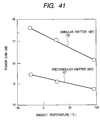
- Fig. 41 shows a result of measuring temperature dependency of power gain of HBT.
- Fig. 41 shows respective results of HBT having a ring-like emitter (hereinafter, abbreviated as ring-like emitter HBT) and HBT having a rectangular emitter (hereinafter, abbreviated as rectangular emitter HBT).
- ring-like emitter HBT ring-like emitter
- rectangular emitter HBT rectangular emitter
- the ring-like emitter HBT is constituted by connecting basic HBT having an emitter area of 132 ⁇ m 2 in 6 rows in parallel and the rectangular emitter HBT is constituted by connecting basic HBT having an emitter area of 108 ⁇ m 2 in 8 rows in parallel. Measuring conditions are such that collector voltage is 3.5 V and frequency is 1.9 GHz.
- the respective temperature coefficients of power gain of the ring-like emitter HBT and the rectangular emitter HBT are -0.012 dB/°C and -0.006 dB/°C.
- the temperature coefficient of power gain is -0.024 dB/°C and in the case of the rectangular emitter HBT, the temperature coefficient of power gain is -0.012 dB/°C.
- a difference of the temperature dependencies of power gain of the ring-like emitter HBT and the rectangular emitter HBT is caused by temperature dependency of base resistance.
- the base resistance is increased with temperature rise.
- the base resistance of the ring-like emitter HBT is larger than that of the rectangular emitter HBT. Therefore, an amount of change in the base resistance with a change in temperature of the ring-like emitter HBT becomes larger than that of the rectangular emitter HBT.
- mismatch with a matching circuit in view of high frequency is increased with temperature rise and the temperature dependency of power gain is also increased.
- a semiconductor device using a bipolar transistor formed above a semiconductor substrate and having an emitter/base junction region having a planar shape in a ring-like shape.
- the semiconductor substrate is a zinc blende type semiconductor substrate having a (100) ( ⁇ 5 degrees) face
- the bipolar transistor is an emitter top type HBT and a base electrode of the HBT is present only on an inner side of the ring-like emitter/base junction region in the ring-like shape.
- a side in parallel with [011] ( ⁇ 5 degrees) is not present, or (2) in a semiconductor device using an emitter top type HBT formed above a zinc blende type semiconductor substrate having a (100) ( ⁇ 5 degrees) face at a surface thereof and having a planar shape in a ring-like shape, a minimum value of a distance, in a [01-1] direction, between an outer periphery of a base/collector junction region of the HBT and an outer periphery of the emitter/base junction region is larger than a minimum value of the distance in [011] direction, (3) in a semiconductor device using an emitter top type HBT formed above a zinc blende type semiconductor substrate having a (100) ( ⁇ 5 degrees) face at a surface thereof and having an emitter/base junction region having a planar shape in a nonring-like shape, a
- a side in parallel with [011] ( ⁇ 5 degrees) is not present at the outer periphery of the emitter/base junction region is that when the planar shape is a polygonal shape, respective sides thereof are not in parallel with [011] ( ⁇ 5 degrees) and includes a case that the planar shape is a circle, an ellipse or a portion thereof (semicircle or the like).
- HBT achieving 2(1)-aspect of the invention is fabricated by successively processing steps of forming an emitter electrode, forming an emitter mesa constituting a mask by the emitter electrode, forming a base electrode, forming an insulating film side wall to side faces of the emitter electrode and the emitter mesa and forming a base mesa constituting a mask by the emitter electrode and the insulating film side wall.
- HBT achieving the first, the second and the third objects of the invention is constituted by a monolithic microwave integrated circuit (hereinafter, described as MMIC) integrated with at least one kind of a capacitor element, a resistor element, an inductance element and a diode.
- MMIC monolithic microwave integrated circuit
- a power amplifier module including a first amplifier circuit constituted by one or more of bipolar transistors connected in parallel and a second amplifier circuit constituted by one or more of bipolar transistors connected in parallel by multiple stage connection wherein the bipolar transistor provided to the first amplifier circuit is a bipolar transistor having base electrodes on both sides of an emitter electrode in a planar arrangement, and the bipolar transistor provided to the second amplifier circuit is a bipolar transistor including a portion in which a base electrode, an emitter electrode and a collector electrode are successively arranged.
- a planar shape of the emitter electrode of the bipolar transistor included by the first amplifier circuit having the base electrodes on both sides of the emitter electrode is a quadrangular shape in a representative shape. Further, a rectangular shape is frequently used.
- the bipolar transistor of the second amplified circuit ordinarily includes a portion in which a base electrode, an emitter electrode and a collector electrode are successively arranged and the emitter electrode includes a portion surrounding at least a portion of the base electrode.
- the planar shape of the emitter electrode of the bipolar transistor includes a closed planar diagram having a space in the inside thereof and having at least one of a curved portion and a linear portion or a portion of the closed planar diagram.
- the base electrode is arranged at a space portion in the inside of the planar diagram of the emitter electrode.
- planar shape of the emitter electrode of the bipolar transistor included by the second amplifier circuit is representatively a ring-like shape or a shape of a portion of a ring-like shape.
- an outer shape of a closed polygonal shape may be used as the ring-like shape.
- first amplifier circuit and the second amplifier circuit may respectively be constituted at separate semiconductor substrates or may be constituted at one semiconductor substrate. This is selected by various items requested in designing a total of the module.
- the first or the second amplifier circuit is used at a driver stage or an output stage in the power amplifier module is sufficiently selected by various items required in designing a total of the module.
- a representative example of a material of an emitter layer material of the bipolar transistor is at least one selected from a group constituting of InGaP, AlGaAs, InP and InGaAlAs.
- fabrication is carried out by successively processing steps of forming an emitter electrode, forming an emitter mesa, forming a base electrode, forming a base mesa and forming a collector electrode.
- the steps are exemplified further specifically in the following.
- a method of fabricating a power amplifier module comprising a step of forming, in a stacked manner, at least a semiconductor layer for a collector, a semiconductor layer for a base above the semiconductor layer for the collector and a semiconductor layer for an emitter above the semiconductor layer for the base above a semiinsulating substrate, a step of forming an emitter electrode having a desired shape above the semiconductor layer for the emitter, a step of forming an emitter region by fabricating the semiconductor layer for the emitter in a mesa shape, a step of forming a base electrode above the semiconductor layer for the base, a step of forming a base region by fabricating the semiconductor layer for the base in a mesa shape mounted with a region including the emitter region in a planar region, and a step of forming a collector electrode and in the steps of fabricating the emitter electrode and the base electrode.
- the invention is provided with the following characteristics.
- the bipolar transistor region included by the first amplifier circuit is planarly arranged with an electrode having the base electrodes on both sides of the emitter electrode in a planar arrangement.
- the bipolar transistor region included by the second amplifier circuit includes a portion successively arranged with the base electrode, the emitter electrode and the collector electrode in a planar arrangement and the emitter electrode is fabricated in a planar arrangement of an electrode having a portion in which the emitter electrode surrounds at least a portion of the base electrode.
- the planar shape and arrangement of the respective electrodes is similar to that in the explanation of the module structure.
- the power amplifier module of the application can enable high power conversion efficiency while sufficiently reducing temperature dependency of power gain under a restriction in constituting the power amplifier module by using a semiconductor element formed above an insulating or a semiinsulating substrate.
- Fig. 1 is a plan structure view of an emitter top HBT which is a first embodiment of the invention.
- a base electrode 2 is arranged on an inner side of a ring-like emitter electrode 1 and a collector electrode 3 is arranged on an outer side thereof. Further, emitter wiring 4 (not illustrated on an inner side of the collector electrode 3), base wiring 5 (not illustrated on the inner side of the collector electrode 3) and collector wiring 6 are connected to the emitter electrode 1, the base electrode 2 and the collector electrode 3 respectively via through holes (not illustrated).
- Figs. 11 and 12 show fabricating steps when HBT shown in Fig. 1 is fabricated by dry etching.
- a highly doped n type GaAs subcollector layer Si concentration 5 ⁇ 10 18 cm -3 , film thickness 0.6 ⁇ m
- an n type GaAs collector layer Si concentration 1x10 1 6 cm -3 , film thickness 0.8 ⁇ m
- a p type GaAs base layer C concentration 3 ⁇ 10 19 cm -3 , film thickness 70 nm
- an n type InGaP emitter layer InP molar ratio 0.5, Si concentration 3 ⁇ 10 17 cm -3 , film thickness 0.2 ⁇ m
- an n type InGaAs cap layer InAs molar ratio 0.5, Si concentration 4 ⁇ 10 19 cm -3 , film thickness 0.2 ⁇ m
- 12 are made to grow above a semiinsulating GaAs substrate (surface (100) ( ⁇ 5 degrees) face) 7 by a metal organic vapor phase epitaxial growth method.
- WSi Si molar ratio 0.3, film thickness 0.3 ⁇ m
- the emitter electrode 1 is formed by dry etching using photolithography and CF 4 .
- the InGaAs cap layer 12 and the InGaP emitter layer 11 are subjected to dry etching by plasma of CH 4 and Cl 2 and the GaAs base layer 10 is exposed.
- the Ti (film thickness 50 nm)/Pt (film thickness 50nm)/Au (film thickness 200 nm) base electrode 2 is formed by a lift-off method (Fig. 11).
- the GaAs base layer 10 and the GaAs collector layer 9 are subjected to dry etching by using photolithography and C 2 F 6 and SF 6 to form the base mesa 14 and expose the GaAs subcollector layer 8.
- the AuGe (film thickness 60 nm)/Ni (film thickness 10 nm)/Au (film thickness 200 nm) collector electrode 3 is formed by a lift-off method and alloyed at 350°C for 30 minutes (Fig. 12).
- wiring is carried out by using deposition of metal, photolithography and milling and an emitter top HBT having a vertical sectional structure shown in Fig. 5 is fabricated.
- a ring-like structure in which an emitter/base junction region is circular is shown as a representative example, the ring-like structure is not necessarily to be circular but arbitrary.
- a ring-like shape shown in Fig. 13 is also possible.
- HBT fabricated on the GaAs substrate
- the embodiment is applicable to all of HBT formed above a zinc blende type semiconductor substrate of InP, GaN, GaP, InSb or the like.
- the base electrode of HBT having the emitter/base junction region the planar shape of which is the ring-like shape is present only on the inner side of the ring-like emitter/base junction region and therefore, the base electrode is limited only to the through hole region and an effect of enabling to realize r ⁇ 2.5 easily is achieved.
- Fig. 4 is a plan structure view of the emitter top HBT which is the second embodiment of the invention.
- the match allowance between the base mesa outer periphery 14 and the emitter electrode 1 is reduced to 0.5 ⁇ m to realize r ⁇ 2.0, at a face taken along line A-A' of Fig. 1, as shown by Fig. 2, an inverse mesa shape appears at the base mesa outer periphery 14.
- a vertical mesa shape shown in Fig. 5 is constituted at a face taken along line B-B' of Fig. 4
- a regular mesa shape shown in Fig. 6 is constituted at a face taken along line C-C' of Fig. 4 and the problem of surface recombination of electrons shown in Fig. 2 is not brought about.
- HBT fabricated above GaAs substrate
- the embodiment is applicable to all of HBT formed above a zinc blende type semiconductor substrate of InP, GaN, GaP, InSb or the like.
- Fig. 7 is a plan structure view of the emitter top HBT which is the third embodiment of the invention.
- a minimum value of a distance between an outer periphery of a base/collector junction region and an outer periphery of an emitter/base junction region of HBT in [01-1] direction becomes larger than a minimum value of the distance in [011] direction.
- match allowance between the base mesa outer periphery 14 and the emitter electrode 1 is set to 0.5 ⁇ m in [011] direction and 1.5 ⁇ m in [01-1] direction.
- wet etching is used in fabricating HBT similar to Embodiment 2.
- a minimum value of a distance between an outer periphery of a base/collector junction region and an outer periphery of an emitter/base junction region of the HBT in [01-1] direction is made to be larger than a minimum value of the distance in [011] direction, as a result, an effect of enabling to easily realize r ⁇ 2.0 is achieved.
- HBT fabricated above a GaAs substrate
- the embodiment is applicable to all of HBT formed above a zinc blende type semiconductor substrate of InP, GaN, GaP, InSb or the like.
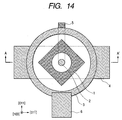
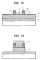
- Figs. 15 through 18 are vertical sectional structure views for explaining a method of fabricating HBT shown in Fig. 14.
- the method is similar to that of Embodiment 1 from crystal growth by the metal organic vapor phase epitaxial growth method to exposure of the GaAs base layer 10 and formation of the base electrode 2.
- an SiO 2 film film thickness 0.5 ⁇ m
- an SiO 2 side wall film thickness 0.3 ⁇ m
- SiO 2 side wall film thickness 0.3 ⁇ m
- a photoresist is formed among emitter fingers and with the photoresist and the exposed emitter electrode 1 and the SiO 2 side wall 15 as a mask, the base mesa 14 is formed.
- etching is carried out by wet etching, since a base mesa orientation is in parallel with ⁇ 010 ⁇ , the mesa shape becomes vertical even when the wet etching is used (Fig. 16).
- the photoresist is removed and the AuGe (film thickness 60 nm)/Ni (film thickness 10 nm)/Au (film thickness 200 nm) collector electrode 3 is formed by the lift-off method and alloyed at 350°C for 30 minutes (Fig. 17).
- wiring is carried out by using deposition of metal, photolithography and milling and the emitter top HBT having a vertical sectional structure shown in Fig. 18 is fabricated.
- HBT fabricated above the GaAs substrate
- the embodiment is applicable to all of HBT formed above a zinc blende type semiconductor substrate of InP, GaN, GaP, InSb or the like.
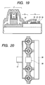
- Fig. 19 is a vertical sectional structure view of MMIC (monolithic microwave integrated circuit) in which HBT 17 satisfying r ⁇ 1.5 is integrated with a resistor element 18 and a capacitor element 19.
- the resistor element 18 comprises a resistor WSiNl layer and the capacitor element 19 comprises three layers of an SiO 2 film 22, an Si 3 N 4 film 23 and an SiO 2 film 24.
- numeral 24 designates a wiring first layer connected from a lower electrode of the capacitor element.
- MMIC includes any one kind of a passive element including an inductance element, a pn junction diode, and a schottkey barrier diode in addition to the resistor element and the capacitor element above the substrate on which HBT 17 is mounted.
- HBT 17 may be a multifinger HBT constituted by connecting in parallel a plurality of pieces of HBTs and Fig. 20 shows an example of a plan structure of the multifinger HBT connected in parallel with four HBTs.
- a ballast resistor may sometimes be added to an emitter or a base of each HBT to avoid nonuniform operation among respective HBTs.
- Fig. 21 is a circuit diagram of MMIC fabricated as a semiconductor device.
- the MMIC is used in the inside of a power amplifier module 32 shown in Fig. 22.
- a glass ceramics substrate sintered at low temperature having a specific inductive capacity of 8 is used in a package of Fig. 22.
- Numeral 25 designates a metal cap and
- numeral 26 designates a chip part.
- Numeral 27 designates a transmission line in which a laminated film of Ag and Pt is formed by thick film screen printing.
- a rear face of the MMIC chip 32 is electrically connected to a ground layer 29 by Ag paste.
- An input/output electrode pad arranged at a surface of the MMIC chip 32 is drawn to the outside of the chip by wire bonding 31.
- Numeral 33 designates a thermal via and numerals 28 and 30 designate the same ground layers as the ground layer 29.
- W-CDMA wide-band code division multiple access system
- an effect of enabling to fabricate the power amplifier having the high power adding efficiency and the high power gain is achieved by using the semiconductor device having as low as a ratio of r ⁇ 1.5.
- a planer shape of the bipolar transistor used in the first amplifier circuit is made in a rectangular emitter shape
- a planar shape of the bipolar transistor used in the second amplifier circuit is made in a ring-like emitter shape and a base electrode thereof is present only on the inner side of the ring-like emitter.
- a planar shape of the bipolar transistor used in the first amplifier circuit is made in a rectangular emitter shape
- a planar shape of the bipolar transistor used in the second amplifier circuit is constituted by an emitter shape which is a portion of. a ring-like shape and a base electrode thereof is present only on the inner side of the ring-like emitter.
- a planar shape of the bipolar transistor is provided with an emitter shape which is a ring-like shape, a base electrode is present only on an inner side of the ring-like emitter and a base thereof is connected to a resistor having a negative temperature coefficient to cancel a change of base resistance.
- a planar shape of the bipolar transistor is provided with an emitter shape which is a portion of a ring-like shape, a base electrode thereof is present only on an inner side of the emitter which is the portion of the ring-like shape and a base thereof is connected to a resistor having a negative temperature coefficient to cancel a change of base resistance.
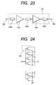
- Fig. 23 is a block diagram of a power amplifier showing the embodiment.
- the example is a power amplifier constituted by two stages.
- numerals 102 and 103 respectively designate a first amplifier circuit and a second amplifier circuit
- numerals 104a, 104b and 104c respectively designate an input matching circuit, an interstage matching circuit and an output matching circuit.
- a high frequency signal to be amplified is inputted from a terminal 122 to the power amplifier, amplified via the matching circuits 104a, 104b, 104c and the amplifier circuits 102 and 103 and thereafter outputted from a terminal 123.
- Fig. 42 and Fig. 43 are respectively a sectional view and a plan view showing a state of mounting a representative power amplifier module.
- a mounting board 160 is mounted with a semiconductor element 151 and a passive element 152.
- Numeral 154 designates a conductive layer constituting connection of an electric signal with the semiconductor element 151. According to the example, a plurality of mounting boards 160, 161 and 162 are stacked to use. Further, the semiconductor element 151 is the above-described power amplifier.
- Fig. 24 shows a circuit diagram of the first amplifier circuit 102.
- the first power amplifier circuit 102 is constituted by eight basic HBTs 105 connected in parallel each having an emitter area of 108 ⁇ m 2 .
- Fig. 24 shows a portion of the basic HBT 105 by surrounding the portion by dotted lines.
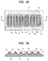
- Fig. 25 shows a planar structure of the amplifier circuit 102 and
- Fig. 26 shows a sectional structure thereof taken along line A-A' in Fig. 25.
- numerals 118, 107, 108, 109, 110 and 119 respectively designate an emitter contact layer, an InGaP emitter layer; a GaAs base layer, a GaAs collector layer, a GaAs subcollector layer and a GaAs substrate.
- numerals 112, 113 and 115 respectively designate an emitter electrode, a base electrode and a collector electrode.
- numerals 111, 116 and 114 respectively designate emitter wiring, base wiring and collector wiring for
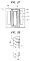
- Fig. 27 shows a detailed plan view of a basic HBT.
- the example shows HBT having a rectangular emitter shape. Respective portions are mounted above the GaAs subcollector 110 formed above the semiinsulating GaAs substrate.
- Numeral 109 designates a collector region, planarly, at a center thereof, the rectangular emitter electrode 112 is formed above the emitter contact layer 118. As shown by the sectional view of Fig. 26, the emitter layer 107 is formed below the emitter contact layer 118. Rectangular regions on both sides of the emitter electrode 112 are the base electrodes 113 and the base region is designated by numeral 108. Rectangular regions present on both sides of the collector region 109 are the collector electrodes 115.
- Fig. 28 shows a circuit diagram of the second amplifier circuit 103.
- the example is constituted by 28 basic HBTs 106 connected in parallel each having a emitter area of 132 ⁇ m 2 .
- Fig. 28 shows a portion of the basic HBT 106 by dotted lines.
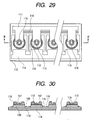
- Fig. 29 shows a plan structure of the amplifier circuit 103 and
- Fig. 8 shows a sectional structure thereof taken along line B-B' of Fig. 29.
- numerals 118, 107, 108, 109, 110 and 119 respectively designate an emitter contact layer, an InGaP emitter layer, a GaAs base layer, a GaAs collector layer, a GaAs subcollector layer and a GaAs substrate.
- numerals 112, 113, 115 respectively designate an emitter electrode, a base electrode and collector electrode.
- numerals 111, 116 and 114 respectively designate emitter wiring, base wiring and collector wiring for connecting respective basic HBT.
- Fig. 31 shows a detailed plan view of a basic HBT.
- the emitter shape is a ring-like shape.
- the example shows HBT in which the base electrode is present only on the inner side of the ring-like emitter. Respective portions are mounted above the GaAs subcollector 110 formed above the GaAs substrate.
- Numeral 109 designates a collector region in a circular shape, planarly, at a center thereof, the emitter electrode 112 in the ring-like shape is formed or the emitter contact layer 118.
- the emitter layer 7 is formed below the emitter contact layer 118.
- the base electrode 113 is arranged on the inner side of the emitter electrode 112 in the ring-like shape.
- Numeral 8 designates the base region. A region present by surrounding the most portion of the collector region 109 is the collector electrode 115.
- the basic HBT used in the second amplifier circuit is representatively shown by the ring-like emitter HBT in the circular shape
- the basic HBT may be HBT which is provided with the emitter shape which is a shape of a portion of a ring-like region shown in Fig. 32 and in which the base electrode is present only on the inner side of an emitter which is a portion of a shape of the ring-like shape.
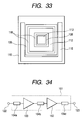
- the basic HBT may be HBT having an emitter shape in a polygonal shape shown in Fig. 33.
- Fig. 33 specifically shows a quadrangular shape, other polygonal shapes can be used.
- Arrangement of respective portions of HBT is similar to that of the example of Fig. 31 and therefore, a detailed explanation thereof will be omitted.
- the shape of the emitter is a ring-like shape or a shape of a portion of a ring-like shape or a polygonal shape or the like and the base electrode may be present only on the inner side of the emitter region.
- the first amplifier circuit 102 constitutes a driver stage and the second amplifier circuit 103 constitutes an output stage
- the same effect is achieved by constituting the output stage by the first amplifier circuit 102 and constituting the driver stage by the second amplifier circuit 3 as shown by Fig. 34.
- the InGaP emitter HBT is -shown as an example of the bipolar transistor used in the power amplifier of the embodiment, according to the invention, a wide range of HBTs of an AlGaAs emitter HBT, an InP emitter HBT using an InP substrate, an InGaAlAs emitter HBT and the like can be used other than the example.
- the amplifier circuit 2 and the amplifier circuit 3 may be formed on the same semiconductor substrate, further, the matching circuits 104a, 104b and 104c may also be formed on a substrate formed with the amplifier circuit 102 and the amplifier circuit 103.
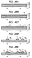
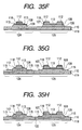
- Figs. 35A through 35H are sectional views of a device showing a method of fabricating a power amplifier in accordance with fabricating steps.
- the embodiment shows a power amplifier constituted by two stages.
- numerals 124 and 125 respectively designate a portion of forming a first amplifier circuit and a portion of forming second amplifier circuit.
- An explanation will be mainly given of a basic HBT below.
- a basic HBT used in the first amplifier circuit is HBT having a rectangular emitter shape and a basic HBT used in the second amplifier circuit is HBT having a ring-like emitter shape.
- an n type GaAs subcollector layer (Si concentration. 5 ⁇ 10 18 cm -3 , film thickness 0.6 ⁇ m) 110, an n-type GaAs collector layer (Si concentration 1 ⁇ 10 16 cm -3 , film thickness 0.8 ⁇ m) 109, a p type GaAs base layer (C concentration 4 ⁇ 10 19 cm -3 , film thickness 90 nm) 108, an n-type InGaP emitter layer (InP molar ratio 0.5, Si concentration 3 ⁇ 10 17 cm -3 , film thickness 30 nm) 107 and an n-type InGaAs emitter contact layer (InAs molar ratio 105, Si concentration 1 ⁇ 10 19 cm -3 , film thickness 0.2 ⁇ m) 118 are made to grow above a semiinsulating GaAs substrate 119 by a metal organic vapor phase epitaxial growth method (Fig. 35A).
- WSi (Si molar ratio 0.3, film thickness 0.3 ⁇ m) 112 is deposited over the entire face of a wafer by using a high-frequency sputtering method (Fig. 35B), and the WSi layer is fabricated by dry etching using photolithography and CF 4 to form the emitter electrode 112 (Fig. 35C).
- the n-type InGaAs emitter contact layer 118 and the n-type InGaP emitter layer 107 are fabricated in desired shapes to form the emitter region (Fig. 35D).
- the Ti (film thickness 50 nm)/Pt (film thickness 50 nm/Au (film thickness 200 nm) base electrode 113 is formed (Fig. 35E).
- the collector electrode 115 is formed and alloyed at 350°C for 30 minutes (Fig. 35G).
- the constitution of the collector electrode 115 is a stack of layers of AuGe (film thickness 60 nm)/Ni (film thickness 10 nm)/Au (film thickness 200 nm).
- an isolation groove 120 for isolating elements is formed. Further, wiring connecting the emitter electrodes, the base electrodes, and collector electrodes between the basic HBTs are formed (Fig. 35H). Incidentally, illustrations of the respective wiring are omitted.
- planar shapes of the respective portions of HBT can naturally be embodied in respective modes. Here, the detailed explanation thereof will be omitted.
- Fig. 36 is a block diagram showing an example of a power amplifier constituted by two stages.
- numerals 102 and 103 respectively designate a first amplifier circuit and a second amplifier circuit.
- numerals 104a, 104b and 104c respectively designate an input matching circuit, an interstage matching circuit and an output matching circuit.
- a high frequency signal to be amplified is inputted from a terminal 122 to the power amplifier, amplified via the matching circuits 104a, 104b and 104c and the amplifier circuits 102 and 103 and outputted from a terminal 123.
- the first amplifier circuit 102 is constituted by six emitter HBTs connected in parallel each having a planar shape in a rectangular shape as explained in Embodiment 1.
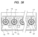
- the second amplifier circuit 103 is constituted by 28 emitter HBTs, connected in parallel, having a planar shape in a ring-like shape as explained in Embodiment 6 or HBTs having emitters each constituting a portion of a ring-like shape and a resistor 117 is connected in series with a base wiring 116 (Fig. 37).
- the example of the resistor is constituted by WSiN. A resistance value thereof at room temperature is 15 ⁇ .
- the resistor 117 may be introduced for each of basic HBTs as shown by Fig. 38. In this case, a value of the WSiN resistor at room temperature is 280 ⁇ .
- the resistance value of the WSiN resistor is an example and differs depending on the required specification of the power amplifier.
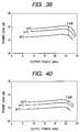
- Fig. 39 and Fig. 40 comparatively show a characteristic of the power amplifier according to the prior art and that according to the present invention, respectively. Measuring conditions is such that frequency is 1.9 GHz, collector voltage is 3.4 V, and ambient temperature falls in a range of -20°C through +85°C.
- Fig. 39 shows a relationship between power gain and output power of the power amplifier of the related art.
- Fig. 39 when the ambient temperature is changed within the range from -20°C to. +85°C, the power gain is changed by 3.3 dB.
- Fig. 40 shows a relationship between power gain and output voltage of the power amplifier according to the invention.
- Fig. 40 when the surrounding temperature is changed within the range from -20°C to +85°C, a change in the power gain is reduced to 2.9 dB. That is, according to the invention, the change in the power gain by temperature is improved by 0.4 dB.
- the power amplifier of high performance having small temperature dependency of the power gain can be provided. Further, according to another aspect of the invention, a method of fabricating the power amplifier of high performance having small temperature dependency of power gain can be provided.
Landscapes
- Engineering & Computer Science (AREA)
- Power Engineering (AREA)
- Bipolar Transistors (AREA)
- Bipolar Integrated Circuits (AREA)
Applications Claiming Priority (4)
| Application Number | Priority Date | Filing Date | Title |
|---|---|---|---|
| JP2002107286 | 2002-04-10 | ||
| JP2002107286A JP2003303827A (ja) | 2002-04-10 | 2002-04-10 | 半導体装置及びその製造方法 |
| JP2003063047A JP2004274430A (ja) | 2003-03-10 | 2003-03-10 | 電力増幅器モジュール及びその製造方法 |
| JP2003063047 | 2003-03-10 |
Publications (2)
| Publication Number | Publication Date |
|---|---|
| EP1353384A2 true EP1353384A2 (de) | 2003-10-15 |
| EP1353384A3 EP1353384A3 (de) | 2005-01-12 |
Family
ID=28456377
Family Applications (1)
| Application Number | Title | Priority Date | Filing Date |
|---|---|---|---|
| EP03008125A Withdrawn EP1353384A3 (de) | 2002-04-10 | 2003-04-07 | Heteroübergang-Bipolartransistor, Verfahren zu seiner Herstellung und Verstärkersmodul |
Country Status (5)
| Country | Link |
|---|---|
| US (1) | US6943387B2 (de) |
| EP (1) | EP1353384A3 (de) |
| KR (1) | KR20030081094A (de) |
| CN (1) | CN1450652A (de) |
| TW (1) | TW200405475A (de) |
Cited By (3)
| Publication number | Priority date | Publication date | Assignee | Title |
|---|---|---|---|---|
| US6943387B2 (en) * | 2002-04-10 | 2005-09-13 | Renesas Technology Corp. | Semiconductor device, manufacturing thereof and power amplifier module |
| CN115148792A (zh) * | 2022-06-27 | 2022-10-04 | 长鑫存储技术有限公司 | 半导体器件及其制备方法 |
| US20230318543A1 (en) * | 2020-12-04 | 2023-10-05 | Murata Manufacturing Co., Ltd. | Power amplifier |
Families Citing this family (21)
| Publication number | Priority date | Publication date | Assignee | Title |
|---|---|---|---|---|
| JP2004146748A (ja) * | 2002-10-28 | 2004-05-20 | Alps Electric Co Ltd | 薄膜キャパシタ素子 |
| JP2004296567A (ja) * | 2003-03-26 | 2004-10-21 | Renesas Technology Corp | 半導体装置およびその製造方法 |
| WO2006058408A1 (en) * | 2004-09-21 | 2006-06-08 | Timeplay Entertainment Corporation | System, method and handheld controller for multi-player gaming |
| JP2006129443A (ja) * | 2004-09-30 | 2006-05-18 | Renesas Technology Corp | 高周波電力増幅器 |
| JP2006156776A (ja) * | 2004-11-30 | 2006-06-15 | Toshiba Corp | 半導体装置 |
| JP2006165248A (ja) * | 2004-12-07 | 2006-06-22 | Renesas Technology Corp | 半導体装置およびその製造方法 |
| US7439608B2 (en) * | 2006-09-22 | 2008-10-21 | Intel Corporation | Symmetric bipolar junction transistor design for deep sub-micron fabrication processes |
| US20080157081A1 (en) * | 2006-12-28 | 2008-07-03 | Samsung Electronics Co., Ltd. | Organic light emitting device and method for manufacturing the same |
| US8020128B2 (en) | 2009-06-29 | 2011-09-13 | International Business Machines Corporation | Scaling of bipolar transistors |
| US8119522B1 (en) | 2010-11-08 | 2012-02-21 | International Business Machines Corporation | Method of fabricating damascene structures |
| CN102244003A (zh) * | 2011-06-20 | 2011-11-16 | 中国科学院微电子研究所 | 一种InP HBT器件侧墙的制备方法 |
| CN103093018B (zh) * | 2011-11-04 | 2016-02-10 | 上海华虹宏力半导体制造有限公司 | 用于提取hbt器件中基区寄生电阻的方法 |
| US10056518B2 (en) * | 2014-06-23 | 2018-08-21 | Qorvo Us, Inc. | Active photonic device having a Darlington configuration |
| CN105261639B (zh) * | 2014-07-18 | 2019-02-26 | 稳懋半导体股份有限公司 | 异质接面双极性电晶体 |
| US9933304B2 (en) | 2015-10-02 | 2018-04-03 | Qorvo Us, Inc. | Active photonic device having a Darlington configuration with feedback |
| US10147833B2 (en) | 2016-04-15 | 2018-12-04 | Qorvo Us, Inc. | Active photonic device having a Darlington configuration with feedback |
| US11309412B1 (en) * | 2017-05-17 | 2022-04-19 | Northrop Grumman Systems Corporation | Shifting the pinch-off voltage of an InP high electron mobility transistor with a metal ring |
| US10847436B2 (en) * | 2017-10-11 | 2020-11-24 | Murata Manufacturing Co., Ltd. | Power amplifier module |
| JP2020184580A (ja) * | 2019-05-08 | 2020-11-12 | 株式会社村田製作所 | 半導体装置 |
| KR20220036128A (ko) * | 2020-09-15 | 2022-03-22 | 삼성전기주식회사 | 전력 증폭기 시스템 |
| NL2032932B1 (en) * | 2022-09-01 | 2024-03-18 | Ampleon Netherlands Bv | Digital rf amplifier |
Family Cites Families (16)
| Publication number | Priority date | Publication date | Assignee | Title |
|---|---|---|---|---|
| JPH053204A (ja) | 1991-06-26 | 1993-01-08 | Hitachi Ltd | 耐α線半導体装置、半導体集積回路装置および論理計算装置 |
| JP2001118319A (ja) * | 1992-12-15 | 2001-04-27 | Hitachi Ltd | データ再生装置 |
| US6045614A (en) * | 1996-03-14 | 2000-04-04 | Raytheon Company | Method for epitaxial growth of twin-free, (111)-oriented II-VI alloy films on silicon substrates |
| JP3345293B2 (ja) * | 1997-02-27 | 2002-11-18 | 日本電信電話株式会社 | ヘテロ接合型バイポーラトランジスタ |
| US6236071B1 (en) * | 1998-07-30 | 2001-05-22 | Conexant Systems, Inc. | Transistor having a novel layout and an emitter having more than one feed point |
| US6521917B1 (en) * | 1999-03-26 | 2003-02-18 | Matsushita Electric Industrial Co., Ltd. | Semiconductor structures using a group III-nitride quaternary material system with reduced phase separation |
| JP3341740B2 (ja) * | 1999-11-15 | 2002-11-05 | 日本電気株式会社 | ヘテロバイポーラ型トランジスタ及びその製造方法 |
| JP3681942B2 (ja) * | 1999-12-28 | 2005-08-10 | 松下電器産業株式会社 | バイポーラトランジスタの製造方法 |
| US6472680B1 (en) * | 1999-12-31 | 2002-10-29 | Matsushita Electric Industrial Co., Ltd. | Semiconductor structures using a group III-nitride quaternary material system with reduced phase separation |
| US6472679B1 (en) * | 1999-12-31 | 2002-10-29 | Matsushita Electric Industrial Co., Ltd. | Semiconductor structures using a group III-nitride quaternary material system with reduced phase separation and method of fabrication |
| JP2001217404A (ja) | 2000-02-01 | 2001-08-10 | Promos Technol Inc | 深いトレンチキャパシターの製造方法 |
| JP2001230261A (ja) | 2000-02-16 | 2001-08-24 | Nec Corp | 半導体装置及びその製造方法 |
| JP3730873B2 (ja) * | 2000-03-16 | 2006-01-05 | ノースロップ・グラマン・コーポレーション | 片持ちベースを有する超高速ヘテロ接合バイポーラ・トランジスタ |
| JP3421631B2 (ja) * | 2000-03-24 | 2003-06-30 | 富士通カンタムデバイス株式会社 | 半導体集積回路装置およびその製造方法 |
| JP2001345329A (ja) * | 2000-06-01 | 2001-12-14 | Hitachi Ltd | 半導体装置およびそれを用いた電力増幅器 |
| EP1353384A3 (de) * | 2002-04-10 | 2005-01-12 | Hitachi, Ltd. | Heteroübergang-Bipolartransistor, Verfahren zu seiner Herstellung und Verstärkersmodul |
-
2003
- 2003-04-07 EP EP03008125A patent/EP1353384A3/de not_active Withdrawn
- 2003-04-09 KR KR10-2003-0022190A patent/KR20030081094A/ko not_active Withdrawn
- 2003-04-09 US US10/409,455 patent/US6943387B2/en not_active Expired - Fee Related
- 2003-04-10 CN CN03110562A patent/CN1450652A/zh active Pending
- 2003-04-10 TW TW092108235A patent/TW200405475A/zh unknown
Cited By (4)
| Publication number | Priority date | Publication date | Assignee | Title |
|---|---|---|---|---|
| US6943387B2 (en) * | 2002-04-10 | 2005-09-13 | Renesas Technology Corp. | Semiconductor device, manufacturing thereof and power amplifier module |
| US20230318543A1 (en) * | 2020-12-04 | 2023-10-05 | Murata Manufacturing Co., Ltd. | Power amplifier |
| US12494749B2 (en) * | 2020-12-04 | 2025-12-09 | Murata Manufacturing Co., Ltd. | Power amplifier |
| CN115148792A (zh) * | 2022-06-27 | 2022-10-04 | 长鑫存储技术有限公司 | 半导体器件及其制备方法 |
Also Published As
| Publication number | Publication date |
|---|---|
| US6943387B2 (en) | 2005-09-13 |
| TW200405475A (en) | 2004-04-01 |
| KR20030081094A (ko) | 2003-10-17 |
| US20030218185A1 (en) | 2003-11-27 |
| CN1450652A (zh) | 2003-10-22 |
| EP1353384A3 (de) | 2005-01-12 |
Similar Documents
| Publication | Publication Date | Title |
|---|---|---|
| US6943387B2 (en) | Semiconductor device, manufacturing thereof and power amplifier module | |
| JP4056226B2 (ja) | 半導体装置 | |
| JP4977313B2 (ja) | ヘテロ接合バイポーラトランジスタ | |
| US20090194792A1 (en) | Semiconductor device and manufacturing method therefor | |
| US6696711B2 (en) | Semiconductor device and power amplifier using the same | |
| US20100032720A1 (en) | Semiconductor device and radio communication device | |
| JP4216634B2 (ja) | 半導体装置 | |
| US20070134820A1 (en) | Semiconductor device and manufacturing method of the same | |
| US7045877B2 (en) | Semiconductor protection device | |
| US7148557B2 (en) | Bipolar transistor and method for fabricating the same | |
| US20060108665A1 (en) | Semiconductor device, manufacturing method of the same, and electronic device | |
| US20060138459A1 (en) | Semiconductor device, manufacturing method of the same and electronic device | |
| US6881639B2 (en) | Method of manufacturing semiconductor device | |
| US6340618B1 (en) | RF power transistor | |
| US6239475B1 (en) | Vertical bipolar transistor having a field shield between the metallic interconnecting layer and the insulation oxide | |
| JP2004274430A (ja) | 電力増幅器モジュール及びその製造方法 | |
| US20060289896A1 (en) | Semiconductor device and method for fabricating the same | |
| JP2636811B2 (ja) | バイポ−ラトランジスタ及びその製造方法 | |
| JP2003303827A (ja) | 半導体装置及びその製造方法 | |
| JP5543936B2 (ja) | ヘテロ接合バイポーラトランジスタの製造方法、及びヘテロ接合バイポーラトランジスタを用いた電力増幅器 | |
| KR20020031722A (ko) | 이종접합 바이폴라 트랜지스터의 구조 및 그 제조방법 | |
| JP2007035809A (ja) | 半導体装置及びその製造方法 |
Legal Events
| Date | Code | Title | Description |
|---|---|---|---|
| PUAI | Public reference made under article 153(3) epc to a published international application that has entered the european phase |
Free format text: ORIGINAL CODE: 0009012 |
|
| AK | Designated contracting states |
Kind code of ref document: A2 Designated state(s): AT BE BG CH CY CZ DE DK EE ES FI FR GB GR HU IE IT LI LU MC NL PT RO SE SI SK TR |
|
| AX | Request for extension of the european patent |
Extension state: AL LT LV MK |
|
| PUAL | Search report despatched |
Free format text: ORIGINAL CODE: 0009013 |
|
| AK | Designated contracting states |
Kind code of ref document: A3 Designated state(s): AT BE BG CH CY CZ DE DK EE ES FI FR GB GR HU IE IT LI LU MC NL PT RO SE SI SK TR |
|
| AX | Request for extension of the european patent |
Extension state: AL LT LV MK |
|
| 17P | Request for examination filed |
Effective date: 20050707 |
|
| AKX | Designation fees paid |
Designated state(s): DE |
|
| STAA | Information on the status of an ep patent application or granted ep patent |
Free format text: STATUS: THE APPLICATION HAS BEEN WITHDRAWN |
|
| 18W | Application withdrawn |
Effective date: 20070104 |