Background of the invention
Field of the invention
The present invention relates to a semiconductor
device using a heterojunction bipolar transistor
(hereinafter, described as HBT) and a method of
fabricating the semiconductor, particularly to a
semiconductor device for a power amplifier for a mobile
communicating machine and a method of fabricating the
semiconductor device.
Further, the present invention relates to a power
amplifier reducing temperature dependency of power gain
and enabling high power conversion efficiency.
Related Art
In recent years, with rapid growth of demand of a
mobile communicating machine, research and development on
a power amplifier used for the communicating machine has
intensively been carried out. Examples of semiconductor
transistors used for a power amplifier for a mobile
communicating machine include GaAsHBT, GaAs field effect
transistor (hereinafter, described as FET), and SiMOS
(Metal-Oxide-Semiconductor) FET. Among them, GaAsHBT is
centrally used as a transistor for a power amplifier for a
mobile communicating machine since the transistor is
provided with characteristics of being excellent in
linearity of an input/output characteristic, operated only
by a positive power source, dispensed with circuit or part
required for generating a negative power source, having a
high output power density and having a small chip area to
thereby save space and reduce cost.
It is indispensable to reduce base/collector
capacitance per unit emitter area to promote performance
of a power amplifier using GaAsHBT, particularly to
promote power added efficiency, power gain and the like.
For that purpose, it is necessary to reduce a ratio r of a
base/collector junction area per an emitter/base junction
area. A collector top HBT structure is generally known as
a method for reducing r and the structure is disclosed in
IEEE Transaction on Electron Devices Vo. 42 No. 11 (1995)
pp.1897-1902).
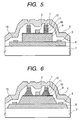
Fig. 3 shows a vertical sectional structure of a
collector top HBT fabricated by the prior art noted above.
As is apparent from the figure, r=1 can be realized,
however, in comparison with an emitter top HBT structure,
there are increased steps of forming a parasitic
emitter/base high resistance region 35, specifically,
steps of ion-implanting boron or the like and annealing,
the fabricating method becomes complicated and therefore,
there poses a problem which amounts to an increase in cost
of a semiconductor device.
Therefore, in order to promote the performance of a
semiconductor device while avoiding an increase in cost,
it is pertinent to achieve a reduction in r by changing
layout of the emitter top HBT. In the case of HBT of the
prior art using a rectangular emitter shape, it has been
difficult to realize r<2.5. This is because a base
electrode and through holes connecting the base electrode
and wiring restruct a rate of reducing the base/collector
junction area. In contrast thereto, r can be reduced by
constituting the base electrode only by a base through
hole region and changing a planar shape of emitter/base
junction from the conventional rectangular shape to a
ring-like structure. Such a ring-like emitter structure
has been proposed in an Si bipolar transistor avoiding an
erroneous operation of software error or the like caused
by irradiation of α-rays and disclosed in JP-A-5-3204.
Although in the prior art of the Si bipolar transistor,
the collector electrode is arranged on an inner side of
the ring-like emitter/base junction, as shown by a plan
structure view of Fig. 1, r<2.5 can be realized by
arranging the base electrode in place of the collector
electrode and arranging the collector electrode on an
outer side of the ring-like emitter/base junction.
It is a first object of the present invention to
provide a semiconductor device using HBT satisfying r<2.5.
It is a second object of the present invention to
provide a semiconductor device using HBT satisfying r<2.0.
It is a third object of the invention to provide a
method of fabricating HBT satisfying r<1.5.
It is a fourth object of the present invention to
provide a semiconductor device having a high power added
efficiency and a high power gain and being suitable for a
power amplifier.
Next, an explanation will be given of a situation
heretofore with regard to a power amplifier. In recent
years, with rapid growth of demand of mobile communicating
apparatus, research and development on a power amplifier
used in a communicating machine has intensively carried
out. Examples of semiconductor transistors used in a
power amplifier for a mobile communicating machine include
a heterojunction bipolar transistor (hereinafter,
abbreviated as HBT), a field effect transistor
(hereinafter, abbreviated as FET), and SiMOS (Metal-Oxide-Semiconductor)
FET. Among them, HBT is provided with
characteristic of being excellent in linearity of an
input/output characteristic, operated only by a positive
power source, dispensed with circuit or part for
generating a negative power source, having a high power
output density and a small chip area to thereby save space
and reduce cost. Therefore, the transistor is centrally
used as a transistor for a power amplifier for a mobile
communicating machine.
To realize high performance formation of a power
amplifier for a mobile communicating machine, high
performance formation of HBT constituting a basic device
thereof is indispensable. For that purpose, it is
necessary to reduce base/collector capacitance. A
technology of using HBT having a ring-like emitter shape
is known as a means therefor in, for example, JP-A-2001-189319.
The technology disclosed in JP-A-2001-189319 has a
difficulty of high temperature dependency of power gain.
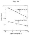
Fig. 41 shows a result of measuring temperature dependency
of power gain of HBT. Fig. 41 shows respective results of
HBT having a ring-like emitter (hereinafter, abbreviated
as ring-like emitter HBT) and HBT having a rectangular
emitter (hereinafter, abbreviated as rectangular emitter
HBT). In both of the ring-like emitter HBT and the
rectangular emitter HBT, a total emitter area is designed
to be equal to about 800 µm2. Further, the ring-like
emitter HBT is constituted by connecting basic HBT having
an emitter area of 132 µm2 in 6 rows in parallel and the
rectangular emitter HBT is constituted by connecting basic
HBT having an emitter area of 108 µm2 in 8 rows in
parallel. Measuring conditions are such that collector
voltage is 3.5 V and frequency is 1.9 GHz. The respective
temperature coefficients of power gain of the ring-like
emitter HBT and the rectangular emitter HBT are -0.012
dB/°C and -0.006 dB/°C. Therefore, when a power amplifier
having two stages constitution is formed, in the case of
the ring-like emitter HBT, the temperature coefficient of
power gain is -0.024 dB/°C and in the case of the
rectangular emitter HBT, the temperature coefficient of
power gain is -0.012 dB/°C.
A difference of the temperature dependencies of
power gain of the ring-like emitter HBT and the
rectangular emitter HBT is caused by temperature
dependency of base resistance. The base resistance is
increased with temperature rise. Meanwhile, the base
resistance of the ring-like emitter HBT is larger than
that of the rectangular emitter HBT. Therefore, an amount
of change in the base resistance with a change in
temperature of the ring-like emitter HBT becomes larger
than that of the rectangular emitter HBT. As a result, in
the case of the ring-like emitter HBT, mismatch with a
matching circuit in view of high frequency is increased
with temperature rise and the temperature dependency of
power gain is also increased.
Based on the background, it is a fifth object of
the present invention to provide a high performance power
amplifier having low temperature dependency of power gain.
In addition thereto, it is a sixth object of the
present invention to provide a method of fabricating a
high performance power amplifier having low temperature
dependency of power gain.
Summary of the invention
In order to achieve the first object of the
invention, according to a semiconductor device related to
the invention, as mentioned in the problem to be resolved
by the invention, there is provide a semiconductor device
using a bipolar transistor formed above a semiconductor
substrate and having an emitter/base junction region
having a planar shape in a ring-like shape. The
semiconductor substrate is a zinc blende type
semiconductor substrate having a (100) (±5 degrees) face,
the bipolar transistor is an emitter top type HBT and a
base electrode of the HBT is present only on an inner side
of the ring-like emitter/base junction region in the ring-like
shape.
Further, in order to achieve the second object of
the invention, (1) at an outer periphery of an
emitter/base junction region of HBT achieving the first
object of the invention, a side in parallel with [011] (±5
degrees) is not present, or (2) in a semiconductor device
using an emitter top type HBT formed above a zinc blende
type semiconductor substrate having a (100) (±5 degrees)
face at a surface thereof and having a planar shape in a
ring-like shape, a minimum value of a distance, in a [01-1]
direction, between an outer periphery of a
base/collector junction region of the HBT and an outer
periphery of the emitter/base junction region is larger
than a minimum value of the distance in [011] direction,
(3) in a semiconductor device using an emitter top type
HBT formed above a zinc blende type semiconductor
substrate having a (100) (±5 degrees) face at a surface
thereof and having an emitter/base junction region having
a planar shape in a nonring-like shape, a minimum value of
a distance, in a [01-1] direction, between an outer
periphery of a base/collector junction region of the HBT
and an outer periphery of the emitter/base junction region
is larger than a minimum value of the distance in [011]
direction. Here, that a side in parallel with [011] (±5
degrees) is not present at the outer periphery of the
emitter/base junction region is that when the planar shape
is a polygonal shape, respective sides thereof are not in
parallel with [011] (±5 degrees) and includes a case that
the planar shape is a circle, an ellipse or a portion
thereof (semicircle or the like).
Further, in order to achieve the third object, HBT
achieving 2(1)-aspect of the invention is fabricated by
successively processing steps of forming an emitter
electrode, forming an emitter mesa constituting a mask by
the emitter electrode, forming a base electrode, forming
an insulating film side wall to side faces of the emitter
electrode and the emitter mesa and forming a base mesa
constituting a mask by the emitter electrode and the
insulating film side wall.
Further, in order to achieve the fourth object of
the invention, HBT achieving the first, the second and the
third objects of the invention is constituted by a
monolithic microwave integrated circuit (hereinafter,
described as MMIC) integrated with at least one kind of a
capacitor element, a resistor element, an inductance
element and a diode.
Next, an explanation will be given of a power
amplifier module.
The gist for achieving the fifth object of the
invention is as follows: That is, there is provided a
power amplifier module including a first amplifier circuit
constituted by one or more of bipolar transistors
connected in parallel and a second amplifier circuit
constituted by one or more of bipolar transistors
connected in parallel by multiple stage connection wherein
the bipolar transistor provided to the first amplifier
circuit is a bipolar transistor having base electrodes on
both sides of an emitter electrode in a planar arrangement,
and the bipolar transistor provided to the second
amplifier circuit is a bipolar transistor including a
portion in which a base electrode, an emitter electrode
and a collector electrode are successively arranged.
A planar shape of the emitter electrode of the
bipolar transistor included by the first amplifier circuit
having the base electrodes on both sides of the emitter
electrode is a quadrangular shape in a representative
shape. Further, a rectangular shape is frequently used.
Further, the bipolar transistor of the second
amplified circuit ordinarily includes a portion in which a
base electrode, an emitter electrode and a collector
electrode are successively arranged and the emitter
electrode includes a portion surrounding at least a
portion of the base electrode. It is general that the
planar shape of the emitter electrode of the bipolar
transistor includes a closed planar diagram having a space
in the inside thereof and having at least one of a curved
portion and a linear portion or a portion of the closed
planar diagram.
Further, the base electrode is arranged at a space
portion in the inside of the planar diagram of the emitter
electrode.
Further, the planar shape of the emitter electrode
of the bipolar transistor included by the second amplifier
circuit is representatively a ring-like shape or a shape
of a portion of a ring-like shape. As mentioned above, an
outer shape of a closed polygonal shape may be used as the
ring-like shape.
Further, the first amplifier circuit and the second
amplifier circuit may respectively be constituted at
separate semiconductor substrates or may be constituted at
one semiconductor substrate. This is selected by various
items requested in designing a total of the module.
Whether the first or the second amplifier circuit
is used at a driver stage or an output stage in the power
amplifier module is sufficiently selected by various items
required in designing a total of the module.
Further, a representative example of a material of
an emitter layer material of the bipolar transistor is at
least one selected from a group constituting of InGaP,
AlGaAs, InP and InGaAlAs.
In order to achieve the sixth object of the
invention, fabrication is carried out by successively
processing steps of forming an emitter electrode, forming
an emitter mesa, forming a base electrode, forming a base
mesa and forming a collector electrode. The steps are
exemplified further specifically in the following.
There are provided a method of fabricating a power
amplifier module comprising a step of forming, in a
stacked manner, at least a semiconductor layer for a
collector, a semiconductor layer for a base above the
semiconductor layer for the collector and a semiconductor
layer for an emitter above the semiconductor layer for the
base above a semiinsulating substrate, a step of forming
an emitter electrode having a desired shape above the
semiconductor layer for the emitter, a step of forming an
emitter region by fabricating the semiconductor layer for
the emitter in a mesa shape, a step of forming a base
electrode above the semiconductor layer for the base, a
step of forming a base region by fabricating the
semiconductor layer for the base in a mesa shape mounted
with a region including the emitter region in a planar
region, and a step of forming a collector electrode and in
the steps of fabricating the emitter electrode and the
base electrode. The invention is provided with the
following characteristics.
More specifically, the bipolar transistor region
included by the first amplifier circuit is planarly
arranged with an electrode having the base electrodes on
both sides of the emitter electrode in a planar
arrangement. Meanwhile, the bipolar transistor region
included by the second amplifier circuit includes a
portion successively arranged with the base electrode, the
emitter electrode and the collector electrode in a planar
arrangement and the emitter electrode is fabricated in a
planar arrangement of an electrode having a portion in
which the emitter electrode surrounds at least a portion
of the base electrode. The planar shape and arrangement
of the respective electrodes is similar to that in the
explanation of the module structure.
In this way, the power amplifier module of the
application can enable high power conversion efficiency
while sufficiently reducing temperature dependency of
power gain under a restriction in constituting the power
amplifier module by using a semiconductor element formed
above an insulating or a semiinsulating substrate.
Brief description of the drawings
Fig. 1 is a plan structure view of an emitter top
HBT used in a semiconductor device which is a first
embodiment of the invention;
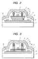
Fig. 2 is a vertical sectional structure view of
the emitter top HBT used in the semiconductor device which
is the first embodiment of the invention (a face taken
along line A-A' of Fig. 1);
Fig. 3 is a vertical sectional structure view of a
collector top HBT which is a prior art;
Fig. 4 is a plan structure view of an emitter top
HBT used in a semiconductor device which is a second
embodiment of the invention;
Fig. 5 is a vertical sectional structure view of
the emitter top HBT used in the semiconductor devices
which are the first and the second embodiment (a face
taken along line B-B' of Fig. 4) of the invention;
Fig. 6 is a vertical sectional structure view of
the emitter top HBT used in the semiconductor device which
is the second embodiment (a face taken along line C-C' of
Fig. 4) of the invention;
Fig. 7 is a plan structure view of an emitter top
HBT used in a semiconductor device which is a third
embodiment of the invention;
Fig. 8 is a vertical sectional structure view (a
face taken along line A-A' of Fig. 7) of the emitter top
HBT used in the semiconductor device which is the third
embodiment of the invention;
Fig. 9 is a plan structure view of the emitter top
HBT used in the semiconductor device which is the third
embodiment of the invention;
Fig. 10 is a plan structure view of an emitter top
HBT used in the semiconductor device which is the third
embodiment of the invention;
Fig. 11 is an explanatory view of a step of
fabricating the emitter top HBT used in the semiconductor
device which is the first embodiment of the invention;
Fig. 12 is an explanatory view of a step of
fabricating the emitter top HBT used in the semiconductor
device which is the first embodiment of the invention;
Fig. 13 is a view with regard to an example of a
plan structure of an emitter top HBT used in the
semiconductor device which is the first embodiment of the
invention;
Fig. 14 is a plan structure view of an emitter top
HBT used in a semiconductor device which is a fourth
embodiment of the invention;
Fig. 15 is an explanatory view of a step of
fabricating the emitter top HBT used in the semiconductor
device which is the fourth embodiment of the invention;
Fig. 16 is an explanatory view of a step of
fabricating the emitter top HBT used in the semiconductor
device which is the fourth embodiment of the invention;
Fig. 17 is an-explanatory view of a step of
fabricating the emitter top HBT used in the semiconductor
device which is the fourth embodiment of the invention;
Fig. 18 is an explanatory view of a step of
fabricating the emitter top HBT used in the semiconductor
device which is the fourth embodiment of the invention;
Fig. 19 is a vertical sectional structure view
showing integrated formation of an emitter top HBT, a
capacitor element and a resistor element in MMIC for a
power amplifier module which is a fifth embodiment of the
invention;
Fig. 20 is a plan structure view of a multifinger
HBT used in MMIC for a power amplifier module which is the
fifth embodiment of the invention;
Fig. 21 is a circuit diagram of MMIC for a power
amplifier comprising two stages of HBT and a bias circuit;
Fig. 22 is a vertical sectional structure view of
the power amplifier module which is the fifth embodiment
of the invention;
Fig. 23 is a block diagram showing a power
amplifier which is an embodiment of the invention;
Fig. 24 is a circuit diagram showing an example of
a first amplifier circuit of a power amplifier which is an
embodiment of the invention;
Fig. 25 is a plan view showing an example of the
first amplifier circuit of the power amplifier which is an
embodiment of the invention;
Fig. 26 is a sectional view showing an example of
the first amplifier circuit of the power amplifier which
is an embodiment of the invention;
Fig. 27 is a plan view showing an example of basic
HBT used in the first amplifier circuit of the power
amplifier which is an embodiment of the invention;
Fig. 28 is a circuit diagram showing an example of
a second amplifier circuit of a power amplifier which is
an embodiment of the invention;
Fig. 29 is a plan view showing an example of the
second amplifier circuit of the power amplifier which is
an embodiment of the invention;
Fig. 30 is a sectional view of a device showing an
example of the second amplifier circuit of the power
amplifier which is an embodiment of the invention;
Fig. 31 is a plan view showing an example of basic
HBT used in the second amplifier circuit of the power
amplifier which is an embodiment of the invention;
Fig. 32 is a plan view showing an example of basic
HBT used in the second amplifier circuit of the power
amplifier which is an embodiment of the invention;
Fig. 33 is a plan view showing an example of basic
HBT used in the second amplifier circuit of the power
amplifier which is an embodiment of the invention;
Fig. 34 is a block diagram showing an example of a
power amplifier which is an embodiment of the invention;
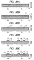
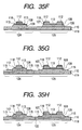
Figs. 35A through 35H are sectional views of a
device showing a method of fabricating a power amplifier
which is an embodiment of the invention in an order of
steps;
Fig. 36 is a block diagram showing an example of a
power amplifier which is other embodiment of the
invention;
Fig. 37 is a plan view showing an example of a
second amplifier circuit of a power amplifier which is
another embodiment of the invention;
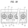
Fig. 38 is a plan view showing an example of a
second amplifier circuit of a power amplifier which is
another embodiment of the invention;
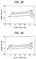
Fig. 39 is a diagram showing a result of measuring
temperature dependency of a characteristic of a power
amplifier having a conventional structure;
Fig. 40 is a diagram showing a result of measuring
temperature dependency of a characteristic of a power
amplifier of the invention;
Fig. 41 is a diagram showing a result of measuring
temperature dependency of power gain of a single one of
HBT;
Fig. 42 is a sectional view showing mounting of a
representative power amplifier module; and
Fig. 43 is a plan view showing mounting of the
representative power amplifier module.
Preferred Embodiments of the invention
Embodiment 1
A description will below be made of an emitter top
HBT which is a. first embodiment of the invention in
reference to Fig. 1, Fig. 11, Fig. 12 and Fig. 13.
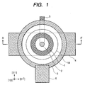
Fig. 1 is a plan structure view of an emitter top
HBT which is a first embodiment of the invention. A base
electrode 2 is arranged on an inner side of a ring-like
emitter electrode 1 and a collector electrode 3 is
arranged on an outer side thereof. Further, emitter
wiring 4 (not illustrated on an inner side of the
collector electrode 3), base wiring 5 (not illustrated on
the inner side of the collector electrode 3) and collector
wiring 6 are connected to the emitter electrode 1, the
base electrode 2 and the collector electrode 3
respectively via through holes (not illustrated). The
ratio r is determined by a distance between a base mesa
outer periphery 14 and the emitter electrode 1 and when
1.0 µm is considered as matching allowance of
photolithography, in the case of the emitter electrode
having a width of, for example, 4.5 µm, r = 2.5 or smaller
can be realized. Further, according to the embodiment,
considering a case of fabricating HBT by using dry etching,
the matching allowance is set to 1.0 µm. When the
matching allowance is set to a value smaller than 1.0 µm,
due to influence of dry etching damage on the base mesa
surface 14, electrons flowing from the emitter to the
collector via the base are recombined on the base mesa 14
and a problem of deteriorating a current gain is brought
about. Although the influence of the damage can be
avoided by using wet etching, the detailed description
thereof will be given in Embodiments 2 and 3.
Figs. 11 and 12 show fabricating steps when HBT
shown in Fig. 1 is fabricated by dry etching. First, a
highly doped n type GaAs subcollector layer (Si
concentration 5×1018 cm-3, film thickness 0.6 µm) 8, an n
type GaAs collector layer (Si concentration 1x101 6cm-3,
film thickness 0.8 µm) 9, a p type GaAs base layer (C
concentration 3×1019 cm-3, film thickness 70 nm) 10, an n
type InGaP emitter layer (InP molar ratio 0.5, Si
concentration 3×1017 cm-3, film thickness 0.2 µm) 11, and an
n type InGaAs cap layer (InAs molar ratio 0.5, Si
concentration 4×1019 cm-3, film thickness 0.2 µm) 12 are
made to grow above a semiinsulating GaAs substrate
(surface (100) (±5 degrees) face) 7 by a metal organic
vapor phase epitaxial growth method. Thereafter, WSi (Si
molar ratio 0.3, film thickness 0.3 µm) is deposited on an
entire face of a wafer by using a high frequency
sputtering method and the emitter electrode 1 is formed by
dry etching using photolithography and CF4. Further, with
the emitter electrode 1 as a mask, the InGaAs cap layer 12
and the InGaP emitter layer 11 are subjected to dry
etching by plasma of CH4 and Cl2 and the GaAs base layer
10 is exposed. Further, the Ti (film thickness 50 nm)/Pt
(film thickness 50nm)/Au (film thickness 200 nm) base
electrode 2 is formed by a lift-off method (Fig. 11).
Thereafter, the GaAs base layer 10 and the GaAs
collector layer 9 are subjected to dry etching by using
photolithography and C2F6 and SF6 to form the base mesa 14
and expose the GaAs subcollector layer 8. Further, the
AuGe (film thickness 60 nm)/Ni (film thickness 10 nm)/Au
(film thickness 200 nm) collector electrode 3 is formed by
a lift-off method and alloyed at 350°C for 30 minutes (Fig.
12). Further, wiring is carried out by using deposition
of metal, photolithography and milling and an emitter top
HBT having a vertical sectional structure shown in Fig. 5
is fabricated.
Although according to the embodiment explained in
reference to Fig. 1, a ring-like structure in which an
emitter/base junction region is circular is shown as a
representative example, the ring-like structure is not
necessarily to be circular but arbitrary. For example, a
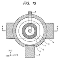
ring-like shape shown in Fig. 13 is also possible.
Further, although according to the embodiment, the
description has been made of HBT fabricated on the GaAs
substrate, the embodiment is applicable to all of HBT
formed above a zinc blende type semiconductor substrate of
InP, GaN, GaP, InSb or the like.
According to the embodiment, the base electrode of
HBT having the emitter/base junction region the planar
shape of which is the ring-like shape is present only on
the inner side of the ring-like emitter/base junction
region and therefore, the base electrode is limited only
to the through hole region and an effect of enabling to
realize r<2.5 easily is achieved.
Embodiment 2
An explanation will below be given of an emitter
top HBT which is a second embodiment of the invention in
reference to Fig. 1, Fig. 2, Fig. 4, Fig. 5 and Fig. 6.
Fig. 4 is a plan structure view of the emitter top
HBT which is the second embodiment of the invention. When
in the ring-like emitter HBT shown in Embodiment 1 (Fig.
1), the match allowance between the base mesa outer
periphery 14 and the emitter electrode 1 is reduced to 0.5
µm to realize r < 2.0, at a face taken along line A-A' of
Fig. 1, as shown by Fig. 2, an inverse mesa shape appears
at the base mesa outer periphery 14. Since the match
allowance between the base mesa outer periphery 14 and the
emitter electrode 1 is small, the GaAs surface having a
high recombination rate is present within a distance of
diffusing electrons at the inside of the collector and the
current gain is deteriorated. Hence, as shown by Fig. 4,
a side in parallel with [011] direction in which the
inverse mesa shape appears is prevented from being present
on the outer periphery of the emitter electrode 1 and the
base mesa outer periphery 14. Thus, a vertical mesa shape
shown in Fig. 5 is constituted at a face taken along line
B-B' of Fig. 4, a regular mesa shape shown in Fig. 6 is
constituted at a face taken along line C-C' of Fig. 4 and
the problem of surface recombination of electrons shown in
Fig. 2 is not brought about.
According to a method of fabricating HBT shown in
Fig. 4, only dry etching of Embodiment 1 is changed to wet
etching, specifically, phosphoric acid: hydrogen peroxide
water: water = 1:2:40 is used for wet etching of a layer
including As and hydrochloric acid is used for wet etching
of a layer including P.
Although the explanation has been given of HBT
fabricated above GaAs substrate, the embodiment is
applicable to all of HBT formed above a zinc blende type
semiconductor substrate of InP, GaN, GaP, InSb or the like.
According to the embodiment, there is achieved an
effect of enabling to easily realize r < 2.0 without dry
etching damage or a deterioration in the current gain
caused by the inverse mesa shape.
Embodiment 3
An explanation will below be given of an emitter
top HBT which is a third embodiment of the invention in
reference to Fig. 7.
Fig. 7 is a plan structure view of the emitter top
HBT which is the third embodiment of the invention.
Although a side in parallel with [011] direction is
present, a minimum value of a distance between an outer
periphery of a base/collector junction region and an outer
periphery of an emitter/base junction region of HBT in
[01-1] direction becomes larger than a minimum value of
the distance in [011] direction. Specifically, match
allowance between the base mesa outer periphery 14 and the
emitter electrode 1 is set to 0.5 µm in [011] direction
and 1.5 µm in [01-1] direction. Further, wet etching is
used in fabricating HBT similar to Embodiment 2.
According to the invention, in a semiconductor
device using an emitter top type HBT formed above a zinc
blende type semiconductor substrate having a (100) (±5
degrees) face at a surface thereof and having an
emitter/base junction region the planar shape of which is
a ring-like shape, a minimum value of a distance between
an outer periphery of a base/collector junction region and
an outer periphery of an emitter/base junction region of
the HBT in [01-1] direction is made to be larger than a
minimum value of the distance in [011] direction, as a
result, an effect of enabling to easily realize r < 2.0 is
achieved.
Also in cases of nonring-like emitters shown in
Figs. 9 and 10, when a minimum value of a distance between
an outer periphery of a base/collector junction region and
an outer periphery of an emitter/base junction region in
[01-1] direction is designed to be larger than a minimum
value of the distance in [011] direction, r < 2.0 can
naturally be realized easily.
Although according to the embodiment, an
explanation has been given of HBT fabricated above a GaAs
substrate, the embodiment is applicable to all of HBT
formed above a zinc blende type semiconductor substrate of
InP, GaN, GaP, InSb or the like.
Embodiment 4
An explanation will below be given of HBT
satisfying r < 1.5 and a method of fabricating the same in
reference to Figs. 14 through 18.
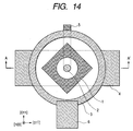
Fig. 14 is a plan structure view of HBT satisfying
r < 1.5. All of the outer periphery of the emitter
electrode 1 is constituted by sides in parallel with {010},
the emitter electrode 1 and the base mesa outer periphery
14 are self-adjustingly formed by an insulating film side
wall 15 and a distance thereof is 0.3 µm. When the width
of the emitter electrode is set to 4.5 µm, r = 1.5.
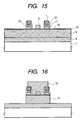
Figs. 15 through 18 are vertical sectional
structure views for explaining a method of fabricating HBT
shown in Fig. 14. The method is similar to that of
Embodiment 1 from crystal growth by the metal organic
vapor phase epitaxial growth method to exposure of the
GaAs base layer 10 and formation of the base electrode 2.
Thereafter, an SiO2 film (film thickness 0.5 µm) is
deposited over the entire face by a plasma excited
chemical vapor phase deposition method and an SiO2 side
wall (film thickness 0.3 µm) 15 is formed by anisotropic
dry etching of SiO2 by using plasma of C2F6 and CHF3 (Fig.
15).
Further, a photoresist is formed among emitter
fingers and with the photoresist and the exposed emitter
electrode 1 and the SiO2 side wall 15 as a mask, the base
mesa 14 is formed. Although etching is carried out by wet
etching, since a base mesa orientation is in parallel with
{010}, the mesa shape becomes vertical even when the wet
etching is used (Fig. 16).
Thereafter, the photoresist is removed and the AuGe
(film thickness 60 nm)/Ni (film thickness 10 nm)/Au (film
thickness 200 nm) collector electrode 3 is formed by the
lift-off method and alloyed at 350°C for 30 minutes (Fig.
17).
Further, wiring is carried out by using deposition
of metal, photolithography and milling and the emitter top
HBT having a vertical sectional structure shown in Fig. 18
is fabricated.
Although according to the embodiment, an
explanation has been given of HBT fabricated above the
GaAs substrate, the embodiment is applicable to all of HBT
formed above a zinc blende type semiconductor substrate of
InP, GaN, GaP, InSb or the like.
According to the embodiment as a result of making
the distance between the base mesa outer periphery 14 and
the emitter electrode 1 proximate to about 0.3µm, an
effect of enabling to easily realize r < 1.5 is achieved.
Embodiment 5
An explanation will below be given of a
semiconductor device which is a fifth embodiment of the
invention and a power amplifier module using the
semiconductor device in reference to Figs. 19 through 21.
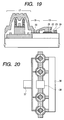
Fig. 19 is a vertical sectional structure view of
MMIC (monolithic microwave integrated circuit) in which
HBT 17 satisfying r < 1.5 is integrated with a resistor
element 18 and a capacitor element 19. The resistor
element 18 comprises a resistor WSiNl layer and the
capacitor element 19 comprises three layers of an SiO2
film 22, an Si3N4 film 23 and an SiO2 film 24. Further,
numeral 24 designates a wiring first layer connected from
a lower electrode of the capacitor element.
MMIC includes any one kind of a passive element
including an inductance element, a pn junction diode, and
a schottkey barrier diode in addition to the resistor
element and the capacitor element above the substrate on
which HBT 17 is mounted. HBT 17 may be a multifinger HBT
constituted by connecting in parallel a plurality of
pieces of HBTs and Fig. 20 shows an example of a plan
structure of the multifinger HBT connected in parallel
with four HBTs. In this case, a ballast resistor may
sometimes be added to an emitter or a base of each HBT to
avoid nonuniform operation among respective HBTs.
Fig. 21 is a circuit diagram of MMIC fabricated as
a semiconductor device. The MMIC is used in the inside of
a power amplifier module 32 shown in Fig. 22. A glass
ceramics substrate sintered at low temperature having a
specific inductive capacity of 8 is used in a package of
Fig. 22. Numeral 25 designates a metal cap and numeral 26
designates a chip part. Numeral 27 designates a
transmission line in which a laminated film of Ag and Pt
is formed by thick film screen printing. A rear face of
the MMIC chip 32 is electrically connected to a ground
layer 29 by Ag paste. An input/output electrode pad
arranged at a surface of the MMIC chip 32 is drawn to the
outside of the chip by wire bonding 31. Numeral 33
designates a thermal via and numerals 28 and 30 designate
the same ground layers as the ground layer 29. As a
result of evaluating a characteristic of the power
amplifier by using a wide-band code division multiple
access system (W-CDMA) signal, significant promotion of
the characteristic of a power adding efficiency of 45% and
a power gain of 28 dB is confirmed in comparison with a
power adding efficiency of 40% and a power gain of 25 dB
when the emitter top HBT of the prior art is used.
According to the embodiment, an effect of enabling
to fabricate the power amplifier having the high power
adding efficiency and the high power gain is achieved by
using the semiconductor device having as low as a ratio of
r < 1.5.
According to the invention, there is achieved an
effect of enabling to realize the semiconductor device
using HBT suitable for fabricating the power amplifier
having the high power adding efficiency and high power
gain in which the ratio is as low as r < 2.5 through r <
1.5.
Next, prior to exemplifying a specific embodiment
of the power amplifier module, further specific modes of
the invention will be enumerated.
In order to achieve the fifth object of the
invention, in the power amplifier according to the
invention, in a multistage amplifier comprising a first
amplifier circuit connected in parallel with at least one
or more of bipolar transistors and a second amplifier
circuit connected in parallel with at least one or more of
bipolar transistors, a planer shape of the bipolar
transistor used in the first amplifier circuit is made in
a rectangular emitter shape, a planar shape of the bipolar
transistor used in the second amplifier circuit is made in
a ring-like emitter shape and a base electrode thereof is
present only on the inner side of the ring-like emitter.
Further, in order to achieve the fifth object of
the invention, in the power amplifier according to the
invention, in a multistage power amplifier comprising a
first amplifier circuit connected in parallel with at
least one or more of bipolar transistors and a second
amplifier circuit connected in parallel with at least one
or more of bipolar transistors, a planar shape of the
bipolar transistor used in the first amplifier circuit is
made in a rectangular emitter shape, a planar shape of the
bipolar transistor used in the second amplifier circuit is
constituted by an emitter shape which is a portion of. a
ring-like shape and a base electrode thereof is present
only on the inner side of the ring-like emitter.
Further, in order to achieve the fifth object of
the invention, in the power amplifier according to the
invention, in an amplifier circuit constituted by one or
more of bipolar transistors connected in parallel, a
planar shape of the bipolar transistor is provided with an
emitter shape which is a ring-like shape, a base electrode
is present only on an inner side of the ring-like emitter
and a base thereof is connected to a resistor having a
negative temperature coefficient to cancel a change of
base resistance.
Further, in order to achieve the fifth object of
the invention, in the power amplifier according to the
invention, in an amplifier circuit constituted by one or
more of bipolar transistors connected in parallel, a
planar shape of the bipolar transistor is provided with an
emitter shape which is a portion of a ring-like shape, a
base electrode thereof is present only on an inner side of
the emitter which is the portion of the ring-like shape
and a base thereof is connected to a resistor having a
negative temperature coefficient to cancel a change of
base resistance.
A detailed description will below be made of a
power amplifier showing a mode for carrying out the
invention and a method of fabricating the power amplifier
in reference to the drawings. Further, in all of the
drawings for explaining the mode for carrying out the
invention, the same characters denote the same functions
and the repeated explanation thereof will be omitted.
<Embodiment 6>
An explanation will be given of a power amplifier
according to Embodiment 6 in reference to the drawings.
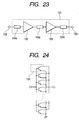
Fig. 23 is a block diagram of a power amplifier showing
the embodiment. The example is a power amplifier
constituted by two stages. In the figure, numerals 102
and 103 respectively designate a first amplifier circuit
and a second amplifier circuit and numerals 104a, 104b and
104c respectively designate an input matching circuit, an
interstage matching circuit and an output matching circuit.
A high frequency signal to be amplified is inputted from a
terminal 122 to the power amplifier, amplified via the
matching circuits 104a, 104b, 104c and the amplifier
circuits 102 and 103 and thereafter outputted from a
terminal 123.
Fig. 42 and Fig. 43 are respectively a sectional
view and a plan view showing a state of mounting a
representative power amplifier module. A mounting board
160 is mounted with a semiconductor element 151 and a
passive element 152. Numeral 154 designates a conductive
layer constituting connection of an electric signal with
the semiconductor element 151. According to the example,
a plurality of mounting boards 160, 161 and 162 are
stacked to use. Further, the semiconductor element 151 is
the above-described power amplifier.
Fig. 24 shows a circuit diagram of the first
amplifier circuit 102. The first power amplifier circuit
102 is constituted by eight basic HBTs 105 connected in
parallel each having an emitter area of 108 µm2. Fig. 24
shows a portion of the basic HBT 105 by surrounding the
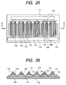
portion by dotted lines. Further, Fig. 25 shows a planar
structure of the amplifier circuit 102 and Fig. 26 shows a
sectional structure thereof taken along line A-A' in Fig.
25. Here, numerals 118, 107, 108, 109, 110 and 119
respectively designate an emitter contact layer, an InGaP
emitter layer; a GaAs base layer, a GaAs collector layer,
a GaAs subcollector layer and a GaAs substrate. Further,
numerals 112, 113 and 115 respectively designate an
emitter electrode, a base electrode and a collector
electrode. Further, numerals 111, 116 and 114
respectively designate emitter wiring, base wiring and
collector wiring for connecting respective basic HBTs.
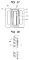
Fig. 27 shows a detailed plan view of a basic HBT.
The example shows HBT having a rectangular emitter shape.
Respective portions are mounted above the GaAs
subcollector 110 formed above the semiinsulating GaAs
substrate. Numeral 109 designates a collector region,
planarly, at a center thereof, the rectangular emitter
electrode 112 is formed above the emitter contact layer
118. As shown by the sectional view of Fig. 26, the
emitter layer 107 is formed below the emitter contact
layer 118. Rectangular regions on both sides of the
emitter electrode 112 are the base electrodes 113 and the
base region is designated by numeral 108. Rectangular
regions present on both sides of the collector region 109
are the collector electrodes 115.
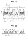
Fig. 28 shows a circuit diagram of the second
amplifier circuit 103. The example is constituted by 28
basic HBTs 106 connected in parallel each having a emitter
area of 132 µm2. Fig. 28 shows a portion of the basic HBT
106 by dotted lines. Fig. 29 shows a plan structure of
the amplifier circuit 103 and Fig. 8 shows a sectional
structure thereof taken along line B-B' of Fig. 29. Here,
numerals 118, 107, 108, 109, 110 and 119 respectively
designate an emitter contact layer, an InGaP emitter layer,
a GaAs base layer, a GaAs collector layer, a GaAs
subcollector layer and a GaAs substrate. Further,
numerals 112, 113, 115 respectively designate an emitter
electrode, a base electrode and collector electrode.
Further, numerals 111, 116 and 114 respectively designate
emitter wiring, base wiring and collector wiring for
connecting respective basic HBT.
Fig. 31 shows a detailed plan view of a basic HBT.
Unlike the example shown in Fig. 25, according to the
example of the basic HBT, the emitter shape is a ring-like
shape. Further, the example shows HBT in which the base
electrode is present only on the inner side of the ring-like
emitter. Respective portions are mounted above the
GaAs subcollector 110 formed above the GaAs substrate.
Numeral 109 designates a collector region in a circular
shape, planarly, at a center thereof, the emitter
electrode 112 in the ring-like shape is formed or the
emitter contact layer 118. As shown by the sectional view
of Fig. 30, the emitter layer 7 is formed below the
emitter contact layer 118. The base electrode 113 is
arranged on the inner side of the emitter electrode 112 in
the ring-like shape. Numeral 8 designates the base region.
A region present by surrounding the most portion of the
collector region 109 is the collector electrode 115.
Further, although in the power amplifier of the
embodiment, the basic HBT used in the second amplifier
circuit, as shown by Fig. 31, is representatively shown by
the ring-like emitter HBT in the circular shape, the basic
HBT may be HBT which is provided with the emitter shape
which is a shape of a portion of a ring-like region shown
in Fig. 32 and in which the base electrode is present only
on the inner side of an emitter which is a portion of a
shape of the ring-like shape.
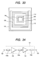
Further, the basic HBT may be HBT having an emitter
shape in a polygonal shape shown in Fig. 33. Although the
example of Fig. 33 specifically shows a quadrangular shape,
other polygonal shapes can be used. Arrangement of
respective portions of HBT is similar to that of the
example of Fig. 31 and therefore, a detailed explanation
thereof will be omitted.
That is, according to the basic HBT used in the
second amplifier circuit, the shape of the emitter is a
ring-like shape or a shape of a portion of a ring-like
shape or a polygonal shape or the like and the base
electrode may be present only on the inner side of the
emitter region.
Further, although according to the power amplifier
of the embodiment, there is shown a case in which the
first amplifier circuit 102 constitutes a driver stage and
the second amplifier circuit 103 constitutes an output
stage, the same effect is achieved by constituting the
output stage by the first amplifier circuit 102 and
constituting the driver stage by the second amplifier
circuit 3 as shown by Fig. 34. However, in this case, it
is necessary to adjust the number of the basic HBTs
arranged in parallel, which is used in each of the
amplifier circuits.
Further, although the InGaP emitter HBT is -shown as
an example of the bipolar transistor used in the power
amplifier of the embodiment, according to the invention, a
wide range of HBTs of an AlGaAs emitter HBT, an InP
emitter HBT using an InP substrate, an InGaAlAs emitter
HBT and the like can be used other than the example.
Further, the amplifier circuit 2 and the amplifier
circuit 3 may be formed on the same semiconductor
substrate, further, the matching circuits 104a, 104b and
104c may also be formed on a substrate formed with the
amplifier circuit 102 and the amplifier circuit 103.
<Embodiment 7>
An explanation will be given of a method of
fabricating a power amplifier by using the embodiment in
reference to the drawings.
Figs. 35A through 35H are sectional views of a
device showing a method of fabricating a power amplifier
in accordance with fabricating steps. The embodiment
shows a power amplifier constituted by two stages. In the
figures, numerals 124 and 125 respectively designate a
portion of forming a first amplifier circuit and a portion
of forming second amplifier circuit. An explanation will
be mainly given of a basic HBT below. According to the
embodiment, a basic HBT used in the first amplifier
circuit is HBT having a rectangular emitter shape and a
basic HBT used in the second amplifier circuit is HBT
having a ring-like emitter shape.
First, an n type GaAs subcollector layer (Si
concentration. 5 × 1018 cm-3, film thickness 0.6 µm) 110, an
n-type GaAs collector layer (Si concentration 1 × 1016 cm-3,
film thickness 0.8 µm) 109, a p type GaAs base layer (C
concentration 4 × 1019 cm-3, film thickness 90 nm) 108, an
n-type InGaP emitter layer (InP molar ratio 0.5, Si
concentration 3×1017 cm-3, film thickness 30 nm) 107 and an
n-type InGaAs emitter contact layer (InAs molar ratio 105,
Si concentration 1 × 1019 cm-3, film thickness 0.2 µm) 118
are made to grow above a semiinsulating GaAs substrate 119
by a metal organic vapor phase epitaxial growth method
(Fig. 35A).
Thereafter, WSi (Si molar ratio 0.3, film thickness
0.3 µm) 112 is deposited over the entire face of a wafer
by using a high-frequency sputtering method (Fig. 35B),
and the WSi layer is fabricated by dry etching using
photolithography and CF4 to form the emitter electrode 112
(Fig. 35C).
Thereafter, the n-type InGaAs emitter contact layer
118 and the n-type InGaP emitter layer 107 are fabricated
in desired shapes to form the emitter region (Fig. 35D).
An example of the fabricating method is as follows: An
unnecessary region of the n-type InGaAs emitter contact
layer 118 is removed by wet etching using photolithography
and an etching solution (an example of a composition of
the etching solution: phosphoric acid: hydrogen peroxide
water: water = 1:2:40). Successively, an unnecessary
region of the n-type InGaAs emitter layer 107 is removed
by wet etching using hydrochloric acid.
Thereafter, by using an ordinary lift-off method,
the Ti (film thickness 50 nm)/Pt (film thickness 50 nm/Au
(film thickness 200 nm) base electrode 113 is formed (Fig.
35E).
Thereafter, the base region is formed by removing
the p-type GaAs base layer 108 by wet etching using
photolithography and an etching solution (an example of a
composition of the etching solution: phosphoric acid:
hydrogen peroxide water: water = 1:2:40). Further,
etching is carried out as far as the n-type GaAs collector
layer 109 to expose the n-type GaAs subcollector layer 110
(Fig. 35F).
Thereafter, by an ordinary lift-off method, the
collector electrode 115 is formed and alloyed at 350°C for
30 minutes (Fig. 35G). The constitution of the collector
electrode 115 is a stack of layers of AuGe (film thickness
60 nm)/Ni (film thickness 10 nm)/Au (film thickness 200
nm).
Lastly, an isolation groove 120 for isolating
elements is formed. Further, wiring connecting the
emitter electrodes, the base electrodes, and collector
electrodes between the basic HBTs are formed (Fig. 35H).
Incidentally, illustrations of the respective wiring are
omitted.
Further, as explained in Embodiment 6, planar
shapes of the respective portions of HBT can naturally be
embodied in respective modes. Here, the detailed
explanation thereof will be omitted.
<Embodiment 8>
In this embodiment, an explanation will be given of
an example of a power amplifier constituted by combining
various kinds of HBTs using the invention.
Fig. 36 is a block diagram showing an example of a
power amplifier constituted by two stages. In the figure,
numerals 102 and 103 respectively designate a first
amplifier circuit and a second amplifier circuit. Further,
numerals 104a, 104b and 104c respectively designate an
input matching circuit, an interstage matching circuit and
an output matching circuit. A high frequency signal to be
amplified is inputted from a terminal 122 to the power
amplifier, amplified via the matching circuits 104a, 104b
and 104c and the amplifier circuits 102 and 103 and
outputted from a terminal 123.
The first amplifier circuit 102 is constituted by
six emitter HBTs connected in parallel each having a
planar shape in a rectangular shape as explained in
Embodiment 1.
The second amplifier circuit 103 is constituted by
28 emitter HBTs, connected in parallel, having a planar
shape in a ring-like shape as explained in Embodiment 6 or
HBTs having emitters each constituting a portion of a
ring-like shape and a resistor 117 is connected in series
with a base wiring 116 (Fig. 37). The example of the
resistor is constituted by WSiN. A resistance value
thereof at room temperature is 15 Ω. The resistor 117 may
be introduced for each of basic HBTs as shown by Fig. 38.
In this case, a value of the WSiN resistor at room
temperature is 280 Ω. The resistance value of the WSiN
resistor is an example and differs depending on the
required specification of the power amplifier.
<Example of characteristic of power amplifier
module of the invention>
An explanation will be given of a characteristic
and an effect achieved by the invention in reference to
drawings.
Fig. 39 and Fig. 40 comparatively show a
characteristic of the power amplifier according to the
prior art and that according to the present invention,
respectively. Measuring conditions is such that frequency
is 1.9 GHz, collector voltage is 3.4 V, and ambient
temperature falls in a range of -20°C through +85°C.
Fig. 39 shows a relationship between power gain and
output power of the power amplifier of the related art.
As shown by Fig. 39, when the ambient temperature is
changed within the range from -20°C to. +85°C, the power
gain is changed by 3.3 dB. Meanwhile, Fig. 40 shows a
relationship between power gain and output voltage of the
power amplifier according to the invention. As shown by
Fig. 40, when the surrounding temperature is changed
within the range from -20°C to +85°C, a change in the
power gain is reduced to 2.9 dB. That is, according to
the invention, the change in the power gain by temperature
is improved by 0.4 dB.
In this way, in the power amplifier module of the
invention, the power amplifier of high performance having
small temperature dependency of the power gain can be
provided. Further, according to another aspect of the
invention, a method of fabricating the power amplifier of
high performance having small temperature dependency of
power gain can be provided.
An explanation will be given of main numerals to
facilitate the understanding of the drawings.
1···emitter electrode, 2···base electrode, 3···
collector electrode, 4···emitter wiring, 5···base wiring,
6···collector wiring, 7···semiconductor substrate, 8···subcollector
layer, 9···collector layer, 10···base layer,
11···emitter layer, 12···cap layer, 13···interlayer
insulating film, 14···base mesa outer periphery, 15···side
wall, 16···photoresist, 17···emitter top HBT, 18···resistor
element, 19···capacitor element, 20···resistor film, 21, 22,
23···capacitor laminated films, 24···capacitor element
lower electrode wiring, 25···metal cap, 26···chip part,
27···transmission line, 31···bonding wire, 32···MMIC, 33···thermal
via, 28, 29, 30···ground layers, 34···bias line,
35···high resistance parasitic emitter/base region, 36···
collector pad, 37···base pad, 38···via hole pad, 101: power
amplifier, 102: first amplifier circuit, 103: second
amplifier circuit, 104a: input matching circuit, 104b:
interstage matching circuit, 104c: output matching circuit,
105: basic HBT, 106: basic HBT, 107: emitter layer, 108:
base layer, 109: collector layer, 110: subcollector layer,
111: emitter wiring, 112: emitter electrode, 113: base
electrode, 114: collector wiring, 115: collector electrode,
116: base wiring, 117: resistor, 118: emitter contact
layer, 119: semiinsulating GaAs substrate, 120:
temperature dependency of power gain of ring-like emitter
HBT per se, 121: temperature dependency of power gain of
rectangular emitter HBT per se, 122: high frequency signal
input terminal, 123: high frequency signal output terminal,
124: first amplifier circuit forming region, 125: second
amplifier circuit forming region.