EP1306976A1 - Treiberschaltung zur Reduzierung von Rauschen in einem Ausgangspuffer - Google Patents
Treiberschaltung zur Reduzierung von Rauschen in einem Ausgangspuffer Download PDFInfo
- Publication number
- EP1306976A1 EP1306976A1 EP02017984A EP02017984A EP1306976A1 EP 1306976 A1 EP1306976 A1 EP 1306976A1 EP 02017984 A EP02017984 A EP 02017984A EP 02017984 A EP02017984 A EP 02017984A EP 1306976 A1 EP1306976 A1 EP 1306976A1
- Authority
- EP
- European Patent Office
- Prior art keywords
- driver
- xor
- ctrl
- signal
- change
- Prior art date
- Legal status (The legal status is an assumption and is not a legal conclusion. Google has not performed a legal analysis and makes no representation as to the accuracy of the status listed.)
- Granted
Links
- 238000011144 upstream manufacturing Methods 0.000 claims description 5
- 102100040844 Dual specificity protein kinase CLK2 Human genes 0.000 description 9
- 101000749291 Homo sapiens Dual specificity protein kinase CLK2 Proteins 0.000 description 9
- 238000012986 modification Methods 0.000 description 4
- 230000004048 modification Effects 0.000 description 4
- 230000000630 rising effect Effects 0.000 description 4
- 230000007423 decrease Effects 0.000 description 2
- 230000000694 effects Effects 0.000 description 2
- 238000005265 energy consumption Methods 0.000 description 2
- 238000011156 evaluation Methods 0.000 description 2
- 230000008092 positive effect Effects 0.000 description 2
- 206010067482 No adverse event Diseases 0.000 description 1
- 230000004913 activation Effects 0.000 description 1
- 230000003247 decreasing effect Effects 0.000 description 1
- 230000001419 dependent effect Effects 0.000 description 1
- 238000011161 development Methods 0.000 description 1
- 230000018109 developmental process Effects 0.000 description 1
- 230000002349 favourable effect Effects 0.000 description 1
Images

Classifications
-
- H—ELECTRICITY
- H03—ELECTRONIC CIRCUITRY
- H03K—PULSE TECHNIQUE
- H03K19/00—Logic circuits, i.e. having at least two inputs acting on one output; Inverting circuits
- H03K19/0008—Arrangements for reducing power consumption
- H03K19/0016—Arrangements for reducing power consumption by using a control or a clock signal, e.g. in order to apply power supply
-
- H—ELECTRICITY
- H03—ELECTRONIC CIRCUITRY
- H03K—PULSE TECHNIQUE
- H03K19/00—Logic circuits, i.e. having at least two inputs acting on one output; Inverting circuits
- H03K19/003—Modifications for increasing the reliability for protection
- H03K19/00346—Modifications for eliminating interference or parasitic voltages or currents
-
- H—ELECTRICITY
- H03—ELECTRONIC CIRCUITRY
- H03K—PULSE TECHNIQUE
- H03K19/00—Logic circuits, i.e. having at least two inputs acting on one output; Inverting circuits
- H03K19/0175—Coupling arrangements; Interface arrangements
- H03K19/0185—Coupling arrangements; Interface arrangements using field effect transistors only
- H03K19/018585—Coupling arrangements; Interface arrangements using field effect transistors only programmable
Definitions
- the present invention relates to a device according to the Preamble of claim 1, i.e. a driver circuit with a driver and a control device controlling the driver.
- a driver is a circuit made up of one fed to it Signal an identical, but suitable for driving larger loads Signal generated, and this outputs.
- Drivers are only one of an almost unlimited number of possible uses to name, for example in microcontrollers used to inside the microcontroller output generated data from the microcontroller. driver are also integrated in almost all other existing ones Circuits used.
- the present invention is therefore based on the object the driver circuit according to the preamble of the claim 1 in such a way that the power consumption of the Driver as well as the electromagnetic caused by the driver Disturbances can be further reduced.
- the driver circuit according to the invention is characterized by this that the control device depends on the strength of the driver the course of the signal to be driven by the driver and / or depending on the course of the output by the driver Signal modified.
- a driver controlled in this way does not consume more energy and does not generate more interference than it does among the given ones Circumstances is inevitable.
- driver circuits described below are an integral part of a microcontroller, but can also be part of it another program-controlled unit such as a microprocessor or a signal processor. They can also be part of any other built-in Circuit or a non-integrated circuit his.
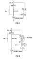
- the first embodiment shown in FIG Contains the type of driver circuits considered here a driver P, a first flip-flop OUT-FF, an XOR gate XOR, and a second flip-flop CTRL-FF.
- the core of the driver circuit shown is driver P.
- the first flip-flop OUT-FF receives one in FIG. 1 signal designated DAT_OUT supplied, generates a identical, but suitable for driving larger loads Signal, and outputs this.
- the remaining components of the Driver circuit, i.e. the XOR gate XOR, and the second Flip-flop CTRL-FF form a control device which the Driver P, more precisely its strength depending on the course control the signal DAT_OUT fed to it.
- the first flip-flop FF-OUT receives a digital input signal DAT_IN supplied, which from the first flip-flop FF-OUT with the rising or falling edge of a clock signal CLK taken over and as the already mentioned signal DAT_OUT to the Driver P is output.
- the signals DAT_IN and DAT_OUT are also used as input signals to the XOR gate XOR fed.
- the XOR gate subjects the fed to it Signals of an XOR operation and gives the result to the second flip-flop CTRL-FF.
- the second flip-flop takes over the signal supplied to it by the XOR gate XOR with increasing or the falling edge of the clock signal CLK and conducts it as a STRONG_DRIVER signal controlling driver P. the driver P further.
- the driver P is replaced by the signal STRONG_DRIVER in a state in which he has a low driver strength having. If and for so long the signal STRONG_DRIVER has the value 1, which is the case when the signals DAT_IN and DAT_OUT in the previous clock signal period had different values, the driver P is replaced by the STRONG_DRIVER signal put in a state in which it has a high driver strength.
- Changes in the level of the driver P supplied and of this signal to be output are both changes from low level to high level as well as changes from high level to low level.
- Switching the driver P from the low driver strength the high driver strength can be achieved, for example, that an additional driver transistor is activated in driver P. becomes; switching the driver P from the high For example, driver strength to the low driver strength in that the additional driver transistor is deactivated again.
- the high driver strength is so large that that from Driver P signal output, especially the contained therein Flanks have a desired course over time.
- driver P only has the high driver strength when the signal to be output changes level no adverse effects on the function of the driver.
- High driver strengths are only during level changes required; the driver comes at all other times even with significantly lower driver strengths.
- the driver P automatically always if no high driver strength is required, into a state in which he has a low driver strength has, the energy consumption of the driver circuit decreases.
- FIG. 2 shows a driver circuit modified in some points shown.
- the driver circuit shown in Figure 2 contains a driver P, a first flip-flop OUT-FF, an XOR gate XOR, an AND gate AND, a second flip-flop CTRL-FF, a third flip-flop CTRL2-FF, and an OR gate OR.
- the core of the driver circuit shown is again the Driver P.
- This receives an in from the first flip-flop OUT-FF fed to the figure 2 designated DAT_OUT generated from it an identical, but larger to drive Load suitable signal, and outputs this.
- the remaining Components of the driver circuit i.e. the XOR gate XOR, the AND gate AND, the second flip-flop CTRL-FF, the third Flip-flop CTRL2-FF, and the OR gate OR form one Control device, the driver P, more specifically its strength depends on the course of the supplied Control signal DAT_OUT.
- the first flip-flop FF-OUT receives a digital input signal DAT_IN supplied, which from the first flip-flop FF-OUT with the rising or falling edge of a first clock signal CLK accepted and as the already mentioned signal DAT_OUT the driver P is output.
- the signals DAT_IN and DAT_OUT are also used as input signals to the XOR gate XOR fed.
- the XOR gate subjects the fed to it Signals of an XOR operation and gives the result to the AND gate AND off.
- the AND gate AND subjects the signals fed to it to an AND operation and outputs the result to the second flip-flop CTRL-FF.
- the second flip-flop CTRL-FF does this for him from the AND gate AND supplied signal with the rising or the falling Edge of the first clock signal CLK and guides the result the OR gate OR and the third flip-flop CTRL2-FF.
- the third flip-flop CTRL2-FF takes over from the first Flip-flop CTRL-FF signal supplied with the rising or the falling edge of a second clock signal CLK2 and conducts it to the OR gate OR.
- the OR gate OR subjects the signals fed to it to an OR operation and gives the result as a signal controlling the driver P. STRONG_DRIVER to driver P.
- the function of the driver circuit according to FIG. 2 corresponds to the rest of the function of the driver circuit according to FIG. 1.
- the modifications of the driver circuits mentioned can consist, for example, that for the second flip-flop CTRL-FF another clock signal (one clock signal with another Clock frequency and / or with a different phase position) is used than for the first flip-flop OUT-FF.
- the signal output by driver P has none abrupt changes, and become none or only low electromagnetic interference or break-in Supply voltage generated.
- driver circuit shown in FIG realize, for example, that the second flip-flop CTRL-FF replaced by a fast clocked shift register which is obtained from the XOR gate XOR Signals in time with a clock signal with a higher frequency than CLK takes over and pushes on, and its elements the current contents of the same as control signals Output control of driver P to this, each these control signals have their own driver transistor within of the driver P can activate and deactivate.
- SR designate the shift register, E1 to E3 the shift register elements, SRIN the shift register SR input signal supplied from the XOR gate, and STRONG_DRIVER1 to STRONG_DRIVER3 that of the shift register generated control signals for controlling the driver.
- driver P that was signal to be driven by driver P is the output signal of a Flip-flops, more precisely the output signal of the flip-flop OUT-FF.
- Control of the driver as described P can also be performed if it is not the case is, for example if the signal to be driven the output signal of a combinatorial logic or another device upstream of the driver. In this case, based on a change in the input signals device upstream of the driver and / or based on the value of an enable signal, which the Driver P and / or the upstream device activated or deactivated, determined whether at all is a signal to drive, and whether that is to be driven Signal will change or may change, and depending on that Driver strength of driver P varies.
- Such a driver circuit is shown in Figure 4, wherein the reference symbol P denotes the driver, K the comparator, FF the first flip-flop, XOR the XOR gate, and CTRL-FF that second flip-flop.
- the determination of whether the signal to be driven and / or the The signal output in front of the driver can also be changed by a combination of the measures described above.
- the driver circuits described make it possible independently from the details of the practical realization that to control drivers contained in it so that its energy consumption and / or the interference caused by this can be reduced to a minimum.
- the realization of the Driver control device by a digital Circuit also allows the occurrence of Glitches or spikes in the signal controlling the driver reliably prevent, and the control device quickly and easy to test.
Landscapes
- Engineering & Computer Science (AREA)
- Computer Hardware Design (AREA)
- Physics & Mathematics (AREA)
- Computing Systems (AREA)
- General Engineering & Computer Science (AREA)
- Mathematical Physics (AREA)
- Logic Circuits (AREA)
Abstract
Description
- den Treiber in Phasen, in welchen sich das zu treibende Signal und/oder das vom Treiber ausgegebene Signal seinen Wert nicht ändert, ändern wird, oder ändern kann, in einen Zustand zu versetzen, in welchem er eine geringe Treiberstärke aufweist, und
- den Treiber in Phasen, in welchen sich das zu treibende Signal und/oder das vom Treiber ausgegebene Signal seinen Wert ändert, ändern wird, oder ändern kann, in einen Zustand zu versetzen, in welchem er eine höhere Treiberstärke aufweist.
- Figur 1
- ein erstes Ausführungsbeispiel der nachfolgend beschriebenen Treiberschaltung,
- Figur 2
- ein zweites Ausführungsbeispiel der nachfolgend näher beschriebenen Treiberschaltung,
- Figur 3
- eine Anordnung, durch welche die Treiberstärke stufenweise erhöht und/oder verringert werden kann, und
- Figur 4
- ein drittes Ausführungsbeispiel der nachfolgend näher beschriebenen Treiberschaltung.
- daß der Treiber P gleichzeitig mit dem Eintreten einer Veränderung des Pegels des ihm zugeführten Signals in einen Zustand versetzt wird, in welchem er eine hohe Treiberstärke aufweist,
- daß der Treiber P für eine Taktsignalperiode in diesem Zustand gehalten wird, und
- daß der Treiber P
- dann, wenn nach der Veränderung des Pegels des ihm zugeführten Signals sofort eine weitere Veränderung erfolgt, für eine weitere Taktsignalperiode in dem Zustand gehalten wird, in welchem er eine hohe Treiberstärke aufweist, bzw.
- dann, wenn nach der Veränderung des Pegels des ihm zugeführten und von ihm auszugebenden Signals nicht sofort eine weitere Veränderung erfolgt, wieder in einen Zustand versetzt wird, in welchem er eine geringe Treiberstärke aufweist, und in diesem Zustand gehalten wird, bis wieder eine Veränderung des Pegels des ihm zugeführten und von ihm auszugebenden Signals erfolgt.
- wobei das UND-Gatter AND und das Signal ACTIVATE eine Aktivierung (ACTIVATE = 1) und Deaktivierung (ACTIVATE = 0) der den Treiber P steuernden Steuervorrichtung ermöglichen, und
- wobei durch das dritte Flip-Flop CTRL2-FF, das ODER-Gatter OR, und das zweite Taktsignal CLK2 bewirkt wird, daß der Zeitpunkt, zu welchem der Treiber aus einem Zustand, in welchem er eine hohe Treiberstärke aufweist, in einen Zustand zurückversetzt wird, in welchem er wieder eine niedrige Treiberstärke aufweist, nach hinten verschoben ist, genauer gesagt - abhängig von der Phasenlage des zweiten Taktsignals CLK2 bezüglich des ersten Taktsignals CLK - um bis zu eine Taktperiode des zweiten Taktsignals CLK2 nach hinten verschoben ist, was den positiven Effekt hat, daß sich auf dem den Treiber P steuernden Signal STRONG_DRIVER keine Spikes bilden können.
- wird der Treiber P zeitgleich mit dem Beginn einer Veränderung des zu treibenden Signals in einen Zustand versetzt, in welchem er eine hohe Treiberstärke aufweist, und
- wird der Treiber P in einen Zustand zurückversetzt, in welchem er eine niedrige Treiberstärke aufweist, nachdem die Veränderung des Wertes des zu treibenden Signals abgeschlossen ist.
- erst nach dem Zeitpunkt, zu welchem sich das zu treibende Signal zu verändern beginnt, in einen Zustand versetzt wird, in welchem er eine hohe Treiberstärke aufweist, und
- bereits vor dem Zeitpunkt, zu welchem die Veränderung des Wertes des zu treibenden Signals abgeschlossen ist, in einen Zustand zurückversetzt wird, in welchem er eine niedrige Treiberstärke aufweist.
- zu Beginn einer Veränderung des zu treibenden Signals wegen der dann noch geringen Treiberstärke der Veränderung des zu treibenden Signals langsam folgt,
- dann der Veränderung des zu treibenden Signals aufgrund der hochgesetzten Treiberstärke schnell folgt, und
- schließlich zum Ende der Veränderung des zu treibenden Signals wegen der dann wieder geringen Treiberstärke der Veränderung des zu treibenden Signals langsam folgt.
- daß das Ausgangssignal des Treibers P einem Komparator zugeführt wird, welcher das Signal 1 ausgibt, wenn das vom Treiber P ausgegebene Signal einen nahe beim dem den Pegel 0 repräsentierenden Potential liegenden ersten Schwellenwert überschreitet, und welcher das Signal 0 ausgibt, wenn das vom Treiber P ausgegebene Signal eine nahe beim dem den Pegel 1 repräsentierenden Potential liegenden zweiten Schwellenwert unterschreitet,
- daß das Ausgangssignal des Komparators einem Flip-Flop zugeführt wird, und
- daß durch eine Gegenüberstellung des Eingangssignals und des Ausgangssignals des Flip-Flops ermittelt wird, ob das Ausgangssignal des Treibers sich gerade ändert, wobei die Auswertung des Eingangssignals und des Ausgangssignals des Flip-Flops wie die Auswertung des Eingangssignals und des Ausgangssignals des zweiten Flip-Flops OUT-FF der Treiberschaltung gemäß Figur 1, also unter Verwendung eines XOR-Gatters und eines zweiten Flip-Flops erfolgt.
- ACTIVATE
- Aktivierungssignal
- AND
- UND-Gatter
- CLK
- Taktsignal
- CLKx
- Taktsignal
- CTRL-FF
- Flip-Flop
- CTRL2-FF
- Flip-Flop
- DAT_IN
- zu treibendes Signal
- DAT_OUT
- zu treibendes Signal
- Ex
- Schieberegister-Element
- FF
- Flip-Flop
- K
- Komparator
- OR
- ODER-Gatter
- OUT-FF
- Flip-Flop
- P
- Treiber
- SR
- Schieberegister
- SRIN
- Eingangssignal von SR
- STRONG_DRIVER
- Steuersignal
- XOR
- XOR-Gatter
Claims (19)
- Treiberschaltung mit einem Treiber (P) und einer den Treiber steuernden Steuervorrichtung (XOR, CTRL-FF; XOR, AND, CTRL-FF, CTRL2-FF, OR; K, FF, XOR, CTRL-FF),
dadurch gekennzeichnet, daß die Steuervorrichtung die Stärke des Treibers abhängig vom Verlauf des durch den Treiber zu treibenden Signals (DAT_OUT) und/oder abhängig vom Verlauf des vom Treiber ausgegebenen Signals modifiziert. - Treiberschaltung nach Anspruch 1,
dadurch gekennzeichnet, daß das zu treibende Signal (DAT_OUT) ein digitales Signal ist. - Treiberschaltung nach Anspruch 1 oder 2,
dadurch gekennzeichnet, daß die Steuervorrichtung (XOR, CTRL-FF; XOR, AND, CTRL-FF, CTRL2-FF, OR; K, FF, XOR, CTRL-FF) zumindest teilweise eine digitale Schaltung ist. - Treiberschaltung nach einem der vorhergehenden Ansprüche,
dadurch gekennzeichnet, daß die Steuervorrichtung (XOR, CTRL-FF; XOR, AND, CTRL-FF, CTRL2-FF, OR; K, FF, XOR, CTRL-FF) eine zumindest teilweise taktgesteuerte Schaltung ist. - Treiberschaltung nach einem der vorhergehenden Ansprüche,
dadurch gekennzeichnet, daß die Steuervorrichtung (XOR, CTRL-FF; XOR, AND, CTRL-FF, CTRL2-FF, OR; K, FF, XOR, CTRL-FF) überprüft, ob das zu treibende Signal (DAT_OUT) und/oder das vom Treiber ausgegebene Signal seinen Wert ändert, ändern wird oder ändern kann, und dann, wenn dieser Fall ist, die Stärke des Treibers (P) modifiziert. - Treiberschaltung nach Anspruch 5,
dadurch gekennzeichnet, daß die Steuervorrichtung (XOR, CTRL-FF; XOR, AND, CTRL-FF, CTRL2-FF, OR; K, FF, XOR, CTRL-FF) davon ausgeht, daß das zu treibende Signal (DAT_OUT) und/oder das vom Treiber (P) ausgegebene Signal seinen Wert ändert, ändern wird, oder ändern kann, wenn sich das Eingangssignal (DAT_IN) und das Ausgangssignal (DAT_OUT) eines vom zu treibenden Signal durchflossenen Flip-Flops (OUT-FF) unterscheiden. - Treiberschaltung nach Anspruch 5,
dadurch gekennzeichnet, daß die Steuervorrichtung (XOR, CTRL-FF; XOR, AND, CTRL-FF, CTRL2-FF, OR; K, FF, XOR, CTRL-FF) davon ausgeht, daß das zu treibende Signal (DAT_OUT) und/oder das vom Treiber (P) ausgegebene Signal seinen Wert ändert, ändern wird, oder ändern kann, wenn sich ein oder mehrere Eingangssignale einer dem Treiber vorgeschalteten Einrichtung verändern. - Treiberschaltung nach Anspruch 5,
dadurch gekennzeichnet, daß die Steuervorrichtung (XOR, CTRL-FF; XOR, AND, CTRL-FF, CTRL2-FF, OR; K, FF, XOR, CTRL-FF) davon ausgeht, daß das zu treibende Signal (DAT_OUT) und/oder das vom Treiber (P) ausgegebene Signal seinen Wert ändert, ändern wird, oder ändern kann, wenn ein Enable-Signal, durch welches der Treiber und/oder eine dem Treiber vorgeschaltete Einrichtung aktivierbar und deaktivierbar sind, einen bestimmten Wert hat. - Treiberschaltung nach einem der vorhergehenden Ansprüche,
dadurch gekennzeichnet, daß die Steuervorrichtung (XOR, CTRL-FF; XOR, AND, CTRL-FF, CTRL2-FF, OR; K, FF, XOR, CTRL-FF) dann, wenn das zu treibende Signal (DAT_OUT) und/oder das vom Treiber (P) ausgegebene Signal seinen Wert ändert, ändern wird, oder ändern kann, den Treiber in einen Zustand versetzt, in welchem er eine höhere Treiberstärke aufweist als es sonst der Fall ist. - Treiberschaltung nach Anspruch 9,
dadurch gekennzeichnet, daß das Versetzen des Treibers (P) in einen Zustand, in welchem er eine höhere Treiberstärke aufweist, erfolgt, bevor das zu treibende Signal (DAT_OUT) und/oder das vom Treiber ausgegebene Signal seinen Wert zu ändern beginnt oder zu ändern beginnen könnte. - Treiberschaltung nach Anspruch 9,
dadurch gekennzeichnet, daß das Versetzen des Treibers (P) in einen Zustand, in welchem er eine höhere Treiberstärke aufweist, genau dann erfolgt, wenn das zu treibende Signal (DAT_OUT) und/oder das vom Treiber ausgegebene Signal seinen Wert zu ändern beginnt oder zu ändern beginnen könnte. - Treiberschaltung nach Anspruch 9,
dadurch gekennzeichnet, daß das Versetzen des Treibers (P) in einen Zustand, in welchem er eine höhere Treiberstärke aufweist, erfolgt, nachdem das zu treibende Signal (DAT_OUT) und/oder das vom Treiber ausgegebene Signal seinen Wert zu ändern beginnt oder zu ändern beginnen könnte. - Treiberschaltung nach einem der Ansprüche 9 bis 12,
dadurch gekennzeichnet, daß die Steuervorrichtung (XOR, CTRL-FF; XOR, AND, CTRL-FF, CTRL2-FF, OR; K, FF, XOR, CTRL-FF) den Treiber (P) so ansteuert, daß die Treiberstärke in aufeinanderfolgenden Schritten stufenweise erhöht wird. - Treiberschaltung nach einem der Ansprüche 9 bis 13,
dadurch gekennzeichnet, daß die Steuervorrichtung (XOR, CTRL-FF; XOR, AND, CTRL-FF, CTRL2-FF, OR; K, FF, XOR, CTRL-FF) dann, wenn das zu treibende Signal (DAT_OUT) und/oder das vom Treiber (P) ausgegebene Signal nach der Erhöhung der Treiberstärke seinen Wert nicht erneut ändert, ändern wird, oder ändern kann, den Treiber in einen Zustand zurückversetzt, in welchem er eine niedrige Treiberstärke aufweist. - Treiberschaltung nach Anspruch 14,
dadurch gekennzeichnet, daß das Zurückversetzen des Treibers (P) in einen Zustand, in welchem er eine niedrige Treiberstärke aufweist, erfolgt, nachdem die Veränderung des Wertes des zu treibenden Signals (DAT_OUT) und/oder des vom Treiber ausgegebene Signals abgeschlossen ist oder abgeschlossen sein könnte. - Treiberschaltung nach Anspruch 14,
dadurch gekennzeichnet, daß das Zurückversetzen des Treibers (P) in einen Zustand, in welchem er eine niedrige Treiberstärke aufweist, genau dann erfolgt, wenn die Veränderung des Wertes des zu treibenden Signals (DAT_OUT) und/oder des vom Treiber ausgegebene Signals abgeschlossen ist oder abgeschlossen sein könnte. - Treiberschaltung nach Anspruch 14,
dadurch gekennzeichnet, daß das Zurückversetzen des Treibers (P) in einen Zustand, in welchem er eine niedrige Treiberstärke aufweist, erfolgt, bevor die Veränderung des Wertes des zu treibenden Signals (DAT_OUT) und/oder des vom Treiber ausgegebene Signals abgeschlossen ist oder abgeschlossen sein könnte. - Treiberschaltung nach einem der Ansprüche 14 bis 17,
dadurch gekennzeichnet, daß die Steuervorrichtung (XOR, CTRL-FF; XOR, AND, CTRL-FF, CTRL2-FF, OR; K, FF, XOR, CTRL-FF) den Treiber (P) so ansteuert, daß die Treiberstärke in aufeinanderfolgenden Schritten stufenweise verringert wird. - Treiberschaltung nach einem der vorhergehenden Ansprüche,
dadurch gekennzeichnet, daß die Steuervorrichtung (XOR, CTRL-FF; XOR, AND, CTRL-FF, CTRL2-FF, OR; K, FF, XOR, CTRL-FF) dann, wenn das zu treibende Signal (DAT_OUT) und/oder das vom Treiber (P) ausgegebene Signal seinen Wert nicht ändert, nicht ändern wird, oder nicht ändern kann, den Treiber in einem Zustand hält, in welchem er eine niedrige Treiberstärke aufweist.
Applications Claiming Priority (2)
| Application Number | Priority Date | Filing Date | Title |
|---|---|---|---|
| DE10142679 | 2001-08-31 | ||
| DE10142679A DE10142679A1 (de) | 2001-08-31 | 2001-08-31 | Treiberschaltung |
Publications (2)
| Publication Number | Publication Date |
|---|---|
| EP1306976A1 true EP1306976A1 (de) | 2003-05-02 |
| EP1306976B1 EP1306976B1 (de) | 2007-02-21 |
Family
ID=7697245
Family Applications (1)
| Application Number | Title | Priority Date | Filing Date |
|---|---|---|---|
| EP02017984A Expired - Lifetime EP1306976B1 (de) | 2001-08-31 | 2002-08-10 | Treiberschaltung zur Reduzierung von Rauschen in einem Ausgangspuffer |
Country Status (3)
| Country | Link |
|---|---|
| US (1) | US20030042929A1 (de) |
| EP (1) | EP1306976B1 (de) |
| DE (2) | DE10142679A1 (de) |
Families Citing this family (2)
| Publication number | Priority date | Publication date | Assignee | Title |
|---|---|---|---|---|
| DE102007048646B3 (de) * | 2007-10-10 | 2009-01-22 | Texas Instruments Deutschland Gmbh | Asynchrones Taktgatter mit Störimpulsschutz |
| ITTO20090334A1 (it) * | 2009-04-28 | 2010-10-29 | St Microelectronics Srl | Dispositivo e metodo di protezione da disturbi per un segnale digitale |
Citations (17)
| Publication number | Priority date | Publication date | Assignee | Title |
|---|---|---|---|---|
| US5149991A (en) * | 1991-06-06 | 1992-09-22 | National Semiconductor Corporation | Ground bounce blocking output buffer circuit |
| EP0533340A2 (de) * | 1991-09-16 | 1993-03-24 | Advanced Micro Devices, Inc. | Ausgangstreiberschaltungen |
| US5285116A (en) * | 1990-08-28 | 1994-02-08 | Mips Computer Systems, Inc. | Low-noise high-speed output buffer and method for controlling same |
| US5319260A (en) * | 1991-07-23 | 1994-06-07 | Standard Microsystems Corporation | Apparatus and method to prevent the disturbance of a quiescent output buffer caused by ground bounce or by power bounce induced by neighboring active output buffers |
| EP0616430A2 (de) * | 1993-03-19 | 1994-09-21 | Advanced Micro Devices, Inc. | Pufferschaltung |
| US5650736A (en) * | 1993-08-20 | 1997-07-22 | Advanced Micro Devices, Inc. | Slew rate controller for high speed bus |
| US5949254A (en) * | 1996-11-26 | 1999-09-07 | Micron Technology, Inc. | Adjustable output driver circuit |
| US5958026A (en) * | 1997-04-11 | 1999-09-28 | Xilinx, Inc. | Input/output buffer supporting multiple I/O standards |
| EP0952668A2 (de) * | 1998-04-20 | 1999-10-27 | Nec Corporation | Stabile Ausgangspufferschaltung bei niedriger Anstiegsgeschwindigkeit |
| WO1999066336A1 (en) * | 1998-06-15 | 1999-12-23 | International Microcircuits, Inc. | Adaptive driver with capacitive load sensing and method of operation |
| US6157204A (en) * | 1998-08-05 | 2000-12-05 | Micron Technology, Inc. | Buffer with adjustable slew rate and a method of providing an adjustable slew rate |
| US6163178A (en) * | 1998-12-28 | 2000-12-19 | Rambus Incorporated | Impedance controlled output driver |
| US6177809B1 (en) * | 1999-05-28 | 2001-01-23 | International Business Machines Corporation | Redundant input/output driver circuit |
| US6208177B1 (en) * | 1999-05-27 | 2001-03-27 | Lucent Technologies Inc. | Output buffer having immediate onset of gentle state transition |
| US6256235B1 (en) * | 2000-06-23 | 2001-07-03 | Micron Technology, Inc. | Adjustable driver pre-equalization for memory subsystems |
| JP2001211063A (ja) * | 1999-11-16 | 2001-08-03 | Ricoh Co Ltd | 出力ドライバ回路 |
| WO2002003553A1 (en) * | 2000-06-30 | 2002-01-10 | Intel Corporation | Buffer with compensating drive strength |
Family Cites Families (11)
| Publication number | Priority date | Publication date | Assignee | Title |
|---|---|---|---|---|
| JPH0720056B2 (ja) * | 1987-12-25 | 1995-03-06 | 日本電気アイシーマイコンシステム株式会社 | 出力回路 |
| US5063308A (en) * | 1988-12-21 | 1991-11-05 | Intel Corporation | Output driver with static and transient parts |
| US5245226A (en) * | 1991-02-25 | 1993-09-14 | Lattice Semiconductor Corporation | Output logic macrocell |
| US6130550A (en) * | 1993-01-08 | 2000-10-10 | Dynalogic | Scaleable padframe interface circuit for FPGA yielding improved routability and faster chip layout |
| EP0665998A4 (de) * | 1993-08-03 | 1996-06-12 | Xilinx Inc | Fpga-schaltkreis mit mikroprozessor. |
| US5621335A (en) * | 1995-04-03 | 1997-04-15 | Texas Instruments Incorporated | Digitally controlled output buffer to incrementally match line impedance and maintain slew rate independent of capacitive output loading |
| US5598119A (en) * | 1995-04-05 | 1997-01-28 | Hewlett-Packard Company | Method and apparatus for a load adaptive pad driver |
| US5869979A (en) * | 1996-04-05 | 1999-02-09 | Altera Corporation | Technique for preconditioning I/Os during reconfiguration |
| EP0926829A1 (de) * | 1997-12-22 | 1999-06-30 | Alcatel | Ausgangsschaltung für digitale integrierte Schaltungen |
| US6281706B1 (en) * | 1998-03-30 | 2001-08-28 | National Semiconductor Corp. | Programmable high speed quiet I/O cell |
| JP3248103B2 (ja) * | 1998-12-04 | 2002-01-21 | 日本プレシジョン・サーキッツ株式会社 | Mosトランジスタ出力回路 |
-
2001
- 2001-08-31 DE DE10142679A patent/DE10142679A1/de not_active Ceased
-
2002
- 2002-08-10 EP EP02017984A patent/EP1306976B1/de not_active Expired - Lifetime
- 2002-08-10 DE DE50209529T patent/DE50209529D1/de not_active Expired - Lifetime
- 2002-09-03 US US10/233,699 patent/US20030042929A1/en not_active Abandoned
Patent Citations (17)
| Publication number | Priority date | Publication date | Assignee | Title |
|---|---|---|---|---|
| US5285116A (en) * | 1990-08-28 | 1994-02-08 | Mips Computer Systems, Inc. | Low-noise high-speed output buffer and method for controlling same |
| US5149991A (en) * | 1991-06-06 | 1992-09-22 | National Semiconductor Corporation | Ground bounce blocking output buffer circuit |
| US5319260A (en) * | 1991-07-23 | 1994-06-07 | Standard Microsystems Corporation | Apparatus and method to prevent the disturbance of a quiescent output buffer caused by ground bounce or by power bounce induced by neighboring active output buffers |
| EP0533340A2 (de) * | 1991-09-16 | 1993-03-24 | Advanced Micro Devices, Inc. | Ausgangstreiberschaltungen |
| EP0616430A2 (de) * | 1993-03-19 | 1994-09-21 | Advanced Micro Devices, Inc. | Pufferschaltung |
| US5650736A (en) * | 1993-08-20 | 1997-07-22 | Advanced Micro Devices, Inc. | Slew rate controller for high speed bus |
| US5949254A (en) * | 1996-11-26 | 1999-09-07 | Micron Technology, Inc. | Adjustable output driver circuit |
| US5958026A (en) * | 1997-04-11 | 1999-09-28 | Xilinx, Inc. | Input/output buffer supporting multiple I/O standards |
| EP0952668A2 (de) * | 1998-04-20 | 1999-10-27 | Nec Corporation | Stabile Ausgangspufferschaltung bei niedriger Anstiegsgeschwindigkeit |
| WO1999066336A1 (en) * | 1998-06-15 | 1999-12-23 | International Microcircuits, Inc. | Adaptive driver with capacitive load sensing and method of operation |
| US6157204A (en) * | 1998-08-05 | 2000-12-05 | Micron Technology, Inc. | Buffer with adjustable slew rate and a method of providing an adjustable slew rate |
| US6163178A (en) * | 1998-12-28 | 2000-12-19 | Rambus Incorporated | Impedance controlled output driver |
| US6208177B1 (en) * | 1999-05-27 | 2001-03-27 | Lucent Technologies Inc. | Output buffer having immediate onset of gentle state transition |
| US6177809B1 (en) * | 1999-05-28 | 2001-01-23 | International Business Machines Corporation | Redundant input/output driver circuit |
| JP2001211063A (ja) * | 1999-11-16 | 2001-08-03 | Ricoh Co Ltd | 出力ドライバ回路 |
| US6256235B1 (en) * | 2000-06-23 | 2001-07-03 | Micron Technology, Inc. | Adjustable driver pre-equalization for memory subsystems |
| WO2002003553A1 (en) * | 2000-06-30 | 2002-01-10 | Intel Corporation | Buffer with compensating drive strength |
Non-Patent Citations (1)
| Title |
|---|
| PATENT ABSTRACTS OF JAPAN vol. 2000, no. 25 12 April 2001 (2001-04-12) * |
Also Published As
| Publication number | Publication date |
|---|---|
| DE50209529D1 (de) | 2007-04-05 |
| DE10142679A1 (de) | 2003-04-03 |
| EP1306976B1 (de) | 2007-02-21 |
| US20030042929A1 (en) | 2003-03-06 |
Similar Documents
| Publication | Publication Date | Title |
|---|---|---|
| DE3689296T2 (de) | Ausgangsschaltung mit Pegelstabilisierung. | |
| DE60216811T2 (de) | Störungsfreie taktauswahlschaltung | |
| DE3851001T2 (de) | Taktgeberschema für ein VLSI-System. | |
| DE2731336A1 (de) | Taktsystem | |
| DE102006045254B4 (de) | Verzögerungsregelschleife für Hochgeschwindigkeits-Halbleiterspeichervorrichtung | |
| DE3022746A1 (de) | Digitale phasenkomparatorschaltung | |
| DE19852457A1 (de) | Verfahren und Vorrichtung zur Phasendrehung in einem Phasenregelkreis | |
| DE2353253A1 (de) | Taktgeber und verfahren zur taktignalerzeugung in einem datenverarbeitungssystem | |
| DE2216123A1 (de) | Verfahren und Anordnung zur Analog Digital Umsetzung unter mehrfacher Inte gration | |
| DE69032145T2 (de) | Schnittstellensteuerungssystem | |
| DE4019659C2 (de) | ||
| EP1039638B1 (de) | Schaltungsanordnung zum störungsfreien Initialisieren von Verzögerungsregelschleifen mit schneller Verriegelung | |
| DE3416548A1 (de) | Verfahren und einrichtung zur optimalen zeitlichen einstellung von taktsignalen fuer digitalrechner | |
| DE69626609T2 (de) | Pipeline-datenverarbeitungsschaltung | |
| DE102007011091A1 (de) | Verfahren zum Testen eines Halbleiterspeichers, Verfahren zur Datenserialisierung und Datenserialisierer | |
| EP1306976B1 (de) | Treiberschaltung zur Reduzierung von Rauschen in einem Ausgangspuffer | |
| DE69422078T2 (de) | Schaltung und Verfahren zum Synchronisieren von Taktsignalen | |
| DE69319454T2 (de) | Verbesserung der Impulse auf einer Signalleitung von integrierten Schaltungen | |
| DE60316182T2 (de) | Signalisierung im Strommodus in einer elektronischen Datenverarbeitungsschaltung | |
| DE19702303A1 (de) | Schaltungsanordnung zum Erzeugen eines Ausgangssignals | |
| DE10227839B4 (de) | Phasendifferenzerfassungsschaltung | |
| DE102010002370A1 (de) | Fehlerdetektion in einer integrierten Schaltung | |
| DE4421419C2 (de) | MOS-Treiberschaltung | |
| EP1361660A2 (de) | Elektronische Schaltung mit mindestens einem Eingang zum Wählen eines Zustands der elektonischen Schaltung | |
| EP1122738A1 (de) | Schaltungsanordnung zur Generierung eines Ausgangs-Taktsignals mit optimierter Signalgenerierungszeit |
Legal Events
| Date | Code | Title | Description |
|---|---|---|---|
| PUAI | Public reference made under article 153(3) epc to a published international application that has entered the european phase |
Free format text: ORIGINAL CODE: 0009012 |
|
| AK | Designated contracting states |
Designated state(s): AT BE BG CH CY CZ DE DK EE ES FI FR GB GR IE IT LI LU MC NL PT SE SK TR |
|
| AX | Request for extension of the european patent |
Extension state: AL LT LV MK RO SI |
|
| 17P | Request for examination filed |
Effective date: 20031024 |
|
| 17Q | First examination report despatched |
Effective date: 20031203 |
|
| AKX | Designation fees paid |
Designated state(s): DE FR IT |
|
| GRAP | Despatch of communication of intention to grant a patent |
Free format text: ORIGINAL CODE: EPIDOSNIGR1 |
|
| GRAS | Grant fee paid |
Free format text: ORIGINAL CODE: EPIDOSNIGR3 |
|
| GRAL | Information related to payment of fee for publishing/printing deleted |
Free format text: ORIGINAL CODE: EPIDOSDIGR3 |
|
| GRAS | Grant fee paid |
Free format text: ORIGINAL CODE: EPIDOSNIGR3 |
|
| GRAA | (expected) grant |
Free format text: ORIGINAL CODE: 0009210 |
|
| AK | Designated contracting states |
Kind code of ref document: B1 Designated state(s): DE FR IT |
|
| REF | Corresponds to: |
Ref document number: 50209529 Country of ref document: DE Date of ref document: 20070405 Kind code of ref document: P |
|
| EN | Fr: translation not filed | ||
| PLBE | No opposition filed within time limit |
Free format text: ORIGINAL CODE: 0009261 |
|
| STAA | Information on the status of an ep patent application or granted ep patent |
Free format text: STATUS: NO OPPOSITION FILED WITHIN TIME LIMIT |
|
| 26N | No opposition filed |
Effective date: 20071122 |
|
| PG25 | Lapsed in a contracting state [announced via postgrant information from national office to epo] |
Ref country code: IT Free format text: LAPSE BECAUSE OF FAILURE TO SUBMIT A TRANSLATION OF THE DESCRIPTION OR TO PAY THE FEE WITHIN THE PRESCRIBED TIME-LIMIT Effective date: 20070221 Ref country code: FR Free format text: LAPSE BECAUSE OF FAILURE TO SUBMIT A TRANSLATION OF THE DESCRIPTION OR TO PAY THE FEE WITHIN THE PRESCRIBED TIME-LIMIT Effective date: 20071012 |
|
| PG25 | Lapsed in a contracting state [announced via postgrant information from national office to epo] |
Ref country code: FR Free format text: LAPSE BECAUSE OF FAILURE TO SUBMIT A TRANSLATION OF THE DESCRIPTION OR TO PAY THE FEE WITHIN THE PRESCRIBED TIME-LIMIT Effective date: 20070221 |
|
| PGFP | Annual fee paid to national office [announced via postgrant information from national office to epo] |
Ref country code: DE Payment date: 20211027 Year of fee payment: 20 |
|
| REG | Reference to a national code |
Ref country code: DE Ref legal event code: R071 Ref document number: 50209529 Country of ref document: DE |