EP1286357B1 - Speicheranordnung mit Dünnfilmtransistoren - Google Patents
Speicheranordnung mit Dünnfilmtransistoren Download PDFInfo
- Publication number
- EP1286357B1 EP1286357B1 EP02255755A EP02255755A EP1286357B1 EP 1286357 B1 EP1286357 B1 EP 1286357B1 EP 02255755 A EP02255755 A EP 02255755A EP 02255755 A EP02255755 A EP 02255755A EP 1286357 B1 EP1286357 B1 EP 1286357B1
- Authority
- EP
- European Patent Office
- Prior art keywords
- gate
- memory cell
- memory
- applying
- insulator
- Prior art date
- Legal status (The legal status is an assumption and is not a legal conclusion. Google has not performed a legal analysis and makes no representation as to the accuracy of the status listed.)
- Expired - Lifetime
Links
Images


Classifications
-
- G—PHYSICS
- G11—INFORMATION STORAGE
- G11C—STATIC STORES
- G11C5/00—Details of stores covered by group G11C11/00
- G11C5/06—Arrangements for interconnecting storage elements electrically, e.g. by wiring
-
- G—PHYSICS
- G11—INFORMATION STORAGE
- G11C—STATIC STORES
- G11C17/00—Read-only memories programmable only once; Semi-permanent stores, e.g. manually-replaceable information cards
- G11C17/14—Read-only memories programmable only once; Semi-permanent stores, e.g. manually-replaceable information cards in which contents are determined by selectively establishing, breaking or modifying connecting links by permanently altering the state of coupling elements, e.g. PROM
- G11C17/16—Read-only memories programmable only once; Semi-permanent stores, e.g. manually-replaceable information cards in which contents are determined by selectively establishing, breaking or modifying connecting links by permanently altering the state of coupling elements, e.g. PROM using electrically-fusible links
Definitions
- the present invention relates in general to a method of writing to a memory array and to a memory array itself.
- Flash memory A conventional example of a non-volatile semiconductor memory suitable for use in portable devices is flash memory.
- Flash memory is described in U.S. Patent No. 4,203,158 to Frohman-Bentchkowsky et al. Flash memory utilizes an insulated floating gate to trap and retain charge over long periods of time. The states of flash memory storage elements represent binary states.
- Conventional flash memory devices, such as the Frohman-Bentchkowsky device are fabricated on silicon wafers in batch processes. Silicon wafers are expensive, raising the cost of the flash memory devices, and batch processes result in low production rates.
- Plastic substrates are generally less expensive than crystal silicon wafers.
- low temperature oxides are used to form the floating gate insulator in these devices. Low temperature oxides are used because of the low melt temperature of the plastic substrate. The volatility of low temperature oxides negatively affects long-term charge storage capability.
- a memory array requires additional circuitry to read and to write to the memory array.
- the fabrication of the circuitry is preferably compatible with memory array fabrication.
- diodes are integrated into the memory cell to simplify the memory system design, at the expense of more complicated manufacturing processes.
- Diodes are also integrated into the peripheral addressing circuits to provide manufacturing compatibility with the memory cells. Diode addressing, however, requires high system power in order to achieve high speed operation.
- a memory device includes a memory array of three terminal thin film transistor (TFT) memory cells.
- the memory cells are coupled to gate lines and data lines.
- the memory cells include a floating gate separated from a gate electrode by an insulator.
- the gate electrode includes a diffusive conductor that diffuses through the insulator under the application of a write voltage.
- the diffusive conductor forms a conductive path through the insulator that couples the gate line to the floating gate, changing the gate capacitance of the memory cell.
- the states of the memory cells are detectable as the differing gate capacitance values for the memory cells.
- the memory cells are three terminal devices, and read currents do not pass through the conductive paths in the memory cells during read operations. This renders the memory cells robust, because read currents do not interfere with the storage mechanism of the memory cells.
- a method of making a memory array comprises forming semiconductor strips over a substrate, forming an insulator over the strips, forming a gate layer over the insulator, patterning the gate layer and the insulator using a mask, forming source/drains using the mask, and forming gate lines over the insulator.
- the gate layer and the insulator are patterned using the same mask as is used to form source/drains in the memory array.
- the use of a single mask reduces the time and cost involved in fabricating the memory array.
- the method of making the memory array can include relatively low temperature processes such as sputter deposition and plasma enhanced chemical vapor deposition. Therefore, the substrate can be made from materials having low melt temperatures such as inexpensive glass or plastics.
- a decoder circuit for the memory device is a NAND decoder circuit used in conjunction with a memory array.
- the NAND decoder circuit and the memory array can be fabricated monolithically with a memory array using self-aligned fabrication methods.
- the memory device can have a high density without a high fabrication cost.
- the integrated address decoder reduces the number of connections required for the memory array to communicate with external devices, such as drivers. This feature is possible because the integrated address decoder can be coupled to each of the lines in the memory array, and may have a relatively small number of output lines connected to output devices.
- the address decoder circuits access the memory cells line-by-line. Therefore, all cells connected to a selected row may be accessed simultaneously. The data rate is therefore much faster than when using single cell access methods.
- the transistor-based address decoder circuit has a low power consumption due to the low power consumption of transistor elements.
- FIG. 1 illustrates a memory device 10.
- the memory device 10 can be, for example, a memory card, and may be based on thin film technology.
- the memory device 10 includes a memory array 100 of memory cells.
- the memory array 100 is coupled to a row address decoder 120 and to a multiplexer 140.
- the multiplexer 140 is coupled to an input/output (I/O) device 150.
- the memory cells (not shown in Figure 1) in the memory array 100 can be three terminal devices, such as, for example, thin film transistor (TFT) devices, and other transistor devices.
- TFT thin film transistor
- the memory array 100 stores data in the memory device 10.
- the address decoder 120 is coupled to gate lines 110 of the memory device 10.
- the address decoder 120 accesses the row of a selected memory cell 200 according to an address instruction.
- the multiplexer 140 is coupled to data lines 130 of the memory array 100.
- the multiplexer 140 combines signals from the data lines 130 and multiplexes the signals to the I/O device 150.
- the I/O device 150 serves as an input receiver and an output buffer for the memory device 10, and communicates with external devices, such as, for example, drivers.
- FIG 2 is a plan view of the TFT memory array 100 illustrated in Figure 1.
- the memory array 100 includes the rows of the gate lines 110, and the columns of the data lines 130.
- Memory cells 200 are located at the crossing points of the data lines 130 and the gate lines 110.
- Each data line 130 is coupled to a p-channel thin film transistor 170 controlled by a gate line 172.
- An exemplary memory cell 200 is discussed in detail with reference to Figures 3A and 3B.
- the memory array 100 includes six gate lines 110 and four data lines 130, intersecting at twenty-four memory cells 200. In practice, any number of gate lines 110, data lines 130, and memory cells 200 can be included in the memory array 100.
- the substrate 160 can be, for example, a semiconductor substrate, such as a single crystalline silicon wafer.
- the single crystalline silicon wafer can include CMOS devices.
- the substrate 160 can be glass, such as, for example, CorningTM 1737.
- the substrate 160 can also be a plastic, such as, for example, polymide. Glass and plastic materials can be used to form the substrate 160 because of the relatively low temperature fabrication method used to produce the memory device 10.
- the data lines 130 can be thin strips of semiconductor material, such as silicon.
- the data lines 130 can be deposited as a silicon layer over the substrate 160, which can be subsequently patterned to form the data line 130 strips.
- the silicon can be an amorphous silicon deposited by, for example, plasma enhanced chemical vapor deposition (PECVD).
- PECVD plasma enhanced chemical vapor deposition
- the silicon strips can be polycrystalline silicon, crystalline silicon, or semiconductors such as SiGe, Ge, SiC, GaAs, and organic semiconductors.
- the data lines 130 can have a thickness on the order of, for example, 1000 Angstroms. The thickness of the data lines 130 may vary according to the material used to form the data lines 130.
- the p-channel TFTs 170 may be used as resistive load elements for the memory array 100.
- the p-channel TFTs 170 may be synchronized with gate line pulses to the memory cells 200, and provide power savings during idle periods for the memory device 10.
- the p-channel TFTs 170 can be replaced with, for example, a simple n-channel circuit, or, a resistive circuit.
- the structure of the memory cells 200 is discussed in detail with reference to Figures 3A and 3B.
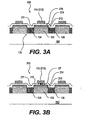
- Figure 3A is a sectional view taken along the section line 3-3 in Figure 2, of a TFT memory cell 200 before a write operation. Neighboring memory cells 200 on the data line 130 are also illustrated.
- Figure 3B is a sectional view taken along the section line 3-3 of the memory cell 200, after a write operation.
- the memory cell 200 is a three terminal transistor device.
- the memory cell 200 may be a thin film transistor formed at the intersection of a gate line 110 and a data line 130.
- the memory array 100 may therefore include a number of memory cells 200 equal to the number of intersections of the gate lines 110 and the data lines 130.
- the memory cell 200 comprises a channel region 132 of the data line 130, a source region 134 of the data line 130, a drain region 136 of the data line 130, a gate insulator 211 having a gate insulator layer 212 disposed over the channel region 132 and a gate insulator layer 216 disposed over a floating gate 214, and a gate line 110 extending over the gate insulator 212.
- the portion of the gate line 110 contacting the gate insulator 216 serves as a gate electrode 218 for the TFT memory cell 200.
- the gate insulator layers 212, 216 may be layers of dielectric material.
- the gate insulators 212, 216 may be separate layers on either side of the floating gate 214, as illustrated in Figures 3A and 3B.
- the gate insulators 212, 216 may be formed as a continuous quantity of dielectric material, with the floating gate 214 embedded within the single layer.
- the gate insulator layers 212, 216 may be made from, for example, silicon dioxide (SiO 2 ), silicon nitride (Si 3 N 4 ), and other dielectrics.
- the gate insulator 211 isolates the gate electrode 218 from the channel region 132 when a voltage is applied to the gate electrode 218.
- the gate insulator 211 may be formed by, for example, a deposition-patterning process.
- the thickness of the gate insulator 211 is selected according to the material used to form the gate insulator 211.
- an oxide gate insulator may have a thickness on the order of 1000 Angstroms
- a silicon nitride gate insulator may have a thickness on the order of 3000 Angstroms.
- the floating gate 214 is made from a conductive material. Examples of materials suitable to form the floating gate 214 include metals such as W, Al, Cr, TiW, and Cu. Alternatively, for example, a doped polysilicon layer, such as a doped polysilicon film, could be used.
- the floating gate 214 can have a thickness on the order of, for example, 300 Angstroms, and can be formed as a strip by patterning and etching processes.
- the gate line 110 (and thus the gate electrode 218) is a conductor including a diffusive metal.
- a diffusive metal is mobile under an applied electric field, and can diffuse through adjacent materials in the direction of the applied field. Examples of suitable materials for the diffusive metal include silver, vanadium, and other diffusive metals.
- the gate line 110 can be formed as a strip by patterning and etching processes. The gate line 110 may be re-etched to be narrower than the floating gate 214, as illustrated in Figures 3A and 3B.
- the source and drain regions 134, 136 can be formed by doping portions of the data line 130, as illustrated in Figures 3A and 3B.
- sources and drains can be formed by depositing a metal-semiconductor alloy, such as, for example, metallic silicide, over the data line 130.
- the memory cells 200 are arranged in a line, and the source region 134 of one memory cell 200 serves as the drain region 136 of a neighboring memory cell 200. Similarly, the drain region 136 of a memory cell 200 serves as the source region 134 of a neighboring memory cell 200. Therefore, each source and each drain is actually a source/drain.
- the portion of the gate line 110 extending over the gate insulator 216 serves as the gate electrode 218 for the memory cell 200, which is a transistor.
- the gate electrode 218 for the memory cell 200 which is a transistor.
- portions of the gate electrode 218 diffuse through the gate insulator 216 to change the gate capacitance of the transistor memory cell 200.
- the change in gate capacitance of the memory cell 200 changes the transistor current-voltage characteristics of the memory cell 200.
- the change in current-voltage characteristics can be detected by current readings from the memory cell 200.
- the read and write functions for the memory cell 200 are discussed in detail below.
- the floating gate 214 is isolated in the gate insulator layers 212, 216. In other words, there are no conductive paths between the gate line 110 and the floating gate 214.
- This state is illustrated by Figure 3A.
- the memory cell 200 has a relatively low gate capacitance Cg.
- the low gate capacitance state of the memory cell 200 before writing can correspond to a binary state of "0" for the memory cell 200. This convention, however, is arbitrary, and the assignment of the binary state of "0” can be reassigned to "1," or any other symbolic value.
- Figure 3B illustrates the memory cell 200 after a write operation.
- the bit in the memory cell 200 can be arbitrarily assigned the binary value of "1," or any other symbolic value.
- the memory cell 200 is written to by applying a driving source potential, such as a high gate voltage, across the memory cell 200.
- the high gate voltage causes conductive elements or portions of the gate electrode 218 to diffuse to the floating gate 214.
- the diffused elements create conductive paths CP as they diffuse through the gate insulator layer 216. .
- the floating gate 214 acts as a diffusion barrier to prevent the diffused metal from the gate electrode 218 from diffusing into the gate insulator layer 212 below the floating gate 214.
- the floating gate 214 is electrically coupled to the gate electrode 218 (and the gate line 110) along the conductive paths CP. This coupling changes the gate capacitance Cg of the memory cell 200.
- the gate capacitance Cg therefore increases after the write operation.
- the change of the gate capacitance Cg is reflected in the transistor transfer characteristics, or source-drain current versus gate voltage (I-V) characteristics of the memory cell 200.
- the I-V characteristics of the memory cells 200 can be detected by, for example, current readings at selected source-drain and gate voltages.
- the memory cells 200 in the memory array 100 are capable of storing two binary states.
- the binary states are detectable as a change in the gate capacitance Cg of the memory cells 200.
- Figure 4 illustrates a transfer characteristic for the TFT memory cell 200 illustrated in Figures 3A and 3B, before and after a write operation.
- the data points illustrated in Figure 4 represent simulated I-V characteristics of an exemplary memory cell 200.
- the I-V curve is derived using an aim-spice model and experimental data from polysilicon TFTs.
- the memory cell 200 is a 1 ⁇ m x 1 ⁇ m memory cell with a gate line 110 width of 0.5 ⁇ m.
- the floating gate 214 is located 20 nm above the channel region 132.
- the transfer curve is under a source-drain voltage of 3 V.
- the source-drain current ratio before and after writing is about 1:9, over a gate voltage value of about 1 V.
- the current ratios in the memory cells 200 are sufficient to distinguish between the states of the memory cells 200 during a read operation.
- FIG 5 is a sectional view of an alternative embodiment of a TFT memory cell 400.
- the TFT memory cell 400 has multiple layers of gate insulator and floating gates.
- the memory cell 400 is capable of storing one of four different memory states, or bits.
- a plurality of memory cells 400 can be included in a memory device, such as in the memory device 10 illustrated in Figure 1.
- the memory cell 400 is a thin film transistor formed at the intersection of a gate line 310 and a data line 330.
- a memory device (not illustrated) could include a number of memory cells 400 equal to the number of intersections of gate lines 310 and data lines 330.
- the portion of the data line 330 of the embodiment illustrated in Figure 5 comprises a semiconductor strip 331, a source electrode 334 disposed over a source contact region 335, a channel region 432, and a drain electrode 336 disposed over a drain contact region 337.
- the transistor memory cell 400 comprises the source and drain electrode and contact regions, a gate insulator 412 comprising layers 412A, 412B, 412C, 412D, floating gates 414A, 414B, 414C, and a gate electrode portion 315 of the gate line 310 extending over the gate insulator layer 412A.
- the gate electrode 315 portion of the gate line 310 contacting the gate insulator layer 412A serves as the gate electrode for the TFT memory cell 400.
- the source and drain electrodes 334, 336 may be formed by depositing a metal-semiconductor alloy, such as, for example, metallic silicide, over the semiconductor strip 331.
- the gate line 310 can comprise a layer 316 of diffusive metal and a layer 318 of conductive metal.
- the conductive layer 318 can be made from, for example, aluminum or copper.
- the conductive layer 318 can be non-diffusive, or less diffusive, than the layer 316 of diffusive metal.
- the conductive layer 318 can therefore serve as a stable bus line for the memory array 100.
- the gate lines 110 in the memory device 10 ( Figure 3A) may have a similar bi-metallic configuration.
- the memory cell 400 includes four gate insulator layers 412A, 412B, 412C, 412D, each of which can be diffused by conductive elements of a diffuse metal.
- Each of the layers 412A, 412B, 412C, 412D can be a layer of dielectric material, and each layer can have a different dielectric constant.
- the use of insulating layers of differing dielectric constants provides flexibility in choosing metal diffusion length and gate capacitance Cg in the memory cell 400.
- the areas of the layers 412A, 412B, 412C, 412D may also be varied.
- a number n + 1 of bit states of can be stored in a memory cell, where n is the number of floating gates in the memory cell.
- four bit states can be stored because the memory cell 400 includes three floating gates 414A, 414B, 414C.
- Each of the four different bit states can be created in the memory cell 400 by applying a selected one of four different write voltages across the memory cell 400.
- the diffusive metals of each of the floating gates 414A, 414B, 414C can be selected to diffuse through an adjacent layer of dielectric material under a different voltage.
- a bi-metallic gate line similar to the gate line 310 can be included in the memory array 100 having memory cells 200.
- the electrodes can be individually patterned over each memory cell 200, 400, beneath a gate line. The electrodes need not extend the full length of the gate lines.
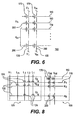
- Figure 6 illustrates a method of writing to a memory cell 200 in the thin film transistor memory array 100.
- the memory cells 200 are illustrated schematically as transistors. There are three characteristic voltages, V l , V m , and V h , used in the write scheme.
- a high gate voltage, V h is applied to the gate line 110 that intersects the selected memory cell 200.
- An intermediate voltage, V m is applied to all other, unselected gate lines 110.
- a low data voltage V l is applied to both ends of the data line 130 intersecting the selected memory cell 200.
- the intermediate voltage V m is applied to both ends of all other, unselected data lines 130.
- the high gate voltage V h relative to the low source and drain voltage V l results in a high voltage field across the selected memory cell 200.
- the high voltage V h ⁇ V l drives diffusion of conductive elements from the gate electrode 218 through the gate insulator 216, electrically connecting the gate electrode 218 (and the gate line 110) to the floating gate 214.
- the coupling of the gate line 110 to the floating gate 214 changes the gate capacitance Cg of the memory cell 200, which is detectable by a read operation.
- the voltage V h ⁇ V m across unselected memory cells 200 on the selected gate line 110 is selected to be insufficient to diffuse gate electrodes 218 of unselected memory cells 200.
- the intermediate voltage V m is insufficient to cause diffusion of gate electrodes 218 of unselected memory cells 200.
- V h may vary between 7, 8, 9 and 10 V to achieve the four bit states of the memory cell 400.
- Other values for the voltages V l , V m , and V h can be used to obtain four bit states in the memory cell 400, depending upon the geometry of and the materials comprising the memory cell 400.
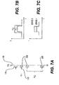
- Figure 7A is a schematic view of a column of the memory array 100 illustrated in Figure 2, including the memory cells 200 coupled to a data line 130 extending along the column.
- the memory cells 200 are illustrated symbolically as transistors.
- Figure 7B illustrates the voltages applied in a reading scheme for a memory cell 200 in the memory array 100.
- Figure 7C illustrates the currents resulting from the reading scheme for the memory array 100.
- the TFT memory cells 200 are connected in series.
- an intermediate voltage V 1 is applied to the gate electrode (i.e., the gate line 110 intersecting the selected memory cell 200) of the selected memory cell 200.
- a high gate voltage V 2 is applied to all other memory cells 200 cells on the column. As illustrated by Figure 7B.
- the state of the bit of the selected memory cell 200 is detectable by detecting the current through the selected data line 130.
- a high current I through the data line 130 can indicate a binary state of "0”
- a low current I through the selected data line 130 can represent a binary state of "1.”
- the p-channel TFTs 170 act as resistive load elements.
- the p-channel TFTs 170 may be synchronized with gate pulses on the gate lines 110 to provide power savings during idle periods of the memory array 100.
- the read operation example discussed above is addressed to a logical NAND arrangement of memory cells 200.
- Other arrangements are possible, such as, for example, a NOR configuration, where the memory cells are connected in parallel to a load.
- the memory cell 400 illustrated in Figure 5 can be read in a manner similar to that of the memory cell 200.
- the states of the memory cells 200 and 400 are detectable as different gate capacitance Cg values for the memory cells 200.
- the memory cells 200 are three terminal devices, so the read current does not pass through the conductive paths CP during read operations.
- the memory cells 200, 400 are therefore more robust, because read currents do not interfere with the storage mechanism in the memory cells 200, 400.
- Figure 8 is a schematic diagram of the address decoder 120 illustrated in Figure 1.
- the address decoder 120 is illustrated as a NAND gate decoder circuit.
- the address decoder 120 addresses the gate lines 110 of the memory array 100.
- the address decoder 120 includes address lines, L 1 , L 2 , ..L M , one address line for each gate line 110 of the memory array 100.
- the address lines L 1 , L 2 , ..L M are each coupled to the gate lines 110 along lines 122 through one or more transistors 124.
- the transistors 124 can be, for example, n-channel transistors.
- V 1 and V 2 are bias voltages.
- a combination of signals are applied to the address lines, L 1 , L 2 , ..L M in order to address a memory cell 200.
- a positive pulse is applied to the address lines L 1 , L 2 , and L 3 .
- the positive pulse turns ON all the n-channel transistors 124 on the address lines L 1 , L 2 , L 3 .
- the voltage on row line R 1 in the memory array is held at a voltage V 1 . Under this condition, the lower voltage V 1 is applied to the gate electrode on row line R 1 and the higher voltage V 2 is applied to the other row lines R 2 -R N .
- N M ! N T ! ( M - N T ) ! where N T is the number of the transistors on each row address line.
- a similar circuit may be also used for a data line decoder for the memory device 10.
- An advantage of using the NAND decoder circuit 120 as illustrated in Figure 8 is that the decoder circuit 120 can be fabricated monolithically with the TFT memory array 100.
- the manufacture of the memory array 100 and the decoder circuit 120 can be performed without via etching, and may include self-aligned TFT fabrication.
- the manufacture of the decoder circuit 120 is therefore compatible with the memory array 100.
- Use of a self-aligned process enables a high density array with a low fabrication cost.
- the decoder circuit 120 is manufactured using transistor devices, the decoder circuit 120 can operate at high speeds with relatively low power requirements.
- all of the memory cells that are connected to the selected row can be accessed simultaneously. This allows high speed parallel reading of and writing to the memory array.
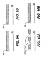
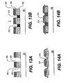
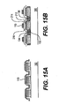
- Figures 9-15 illustrate a method of making a thin film transistor memory array. The construction of the memory array is described with reference to a memory cell and neighboring cells. This method can be used to fabricate the memory array 100, including memory cells 200, as illustrated in Figures 2, 3A and 3B.
- Figures 9A, 10A, 11A, 12A, 13A, 14A and 15A illustrate cross sectional views of the various stages of fabrication of a memory cell 200, as seen from the section line Y-Y' in Figure 2.
- Figures 9B, 10B, 11B, 12B, 13B, 14B and 15B illustrate cross sectional views of the various stages of fabrication of a memory cell 200, as seen from the section line X-X' in Figure 2.
- the fabrication process begins with providing a substrate 160.
- the substrate 160 can be, for example, a semiconductor substrate, such as a single crystalline silicon wafer.
- the single crystalline silicon wafer can include CMOS devices.
- the substrate 160 can be glass, such as, for example, CorningTM 1737.
- the substrate 160 can also be plastic, such as, for example, polymide. Glass and plastic materials can be used to form the substrate 160 because of the relatively low temperature fabrication methods used to produce the memory device 10.
- a semiconductor layer 500 is deposited over the substrate 160.
- the semiconductor layer 500 can be, for example, an amorphous silicon deposited by, for example, PECVD.
- the amorphous silicon can be converted to polycrystalline silicon by a laser or by thermal crystallization.
- the silicon can also be deposited as polycrystalline silicon.
- the silicon strips can be, for example, crystalline silicon, semiconductors such as SiGe, Ge, SiC, GaAs, and organic semiconductors.
- the semiconductor layer 500 can have a thickness on the order of, for example, 1000 Angstroms.
- the semiconductor layer 500 is patterned to form strips 502 extending along columns of the memory array being fabricated.
- the semiconductor layer 500 can be patterned using a photolithographic mask/etch process.
- a dielectric layer 504 is deposited over the substrate 160 and the strips 502.
- the dielectric layer 504 may be, for example, silicon dioxide (SiO 2 ), silicon nitride (Si 3 N 4 ), and other dielectrics.
- the deposition process may be, for example, CVD, PECVD, and other deposition processes.
- the thickness of the dielectric layer 504 is selected according to the material used to form the dielectric layer 504. For example, an oxide dielectric layer 504 may have a thickness on the order of, for example, 1000 Angstroms, while a silicon nitride dielectric layer 504 may have a thickness on the order of, for example, 3000 Angstroms.
- the gate layer 506 may be, for example, a floating gate layer.
- the gate layer 506 can be a conductive material. Examples of materials suitable to form the gate layer 506 include metals such as W, Al, Cr, TiW, and Cu. Alternatively, a doped polysilicon layer, such as a doped polysilicon film, could be used.
- the gate layer 506 can have a thickness on the order of, for example, 300 Angstroms.
- the gate layer 506 can be deposited by, for example, DC or RF sputter deposition processes, and other deposition processes.
- the dielectric layer 504 and the gate layer 506 are patterned. During patterning, a photoresist mask layer 508 is placed over the gate layer 506. The gate layer 506 and the dielectric layer 504 are then etched. The etchant chemical does not etch the strips 502 or the substrate 160.
- regions 510 of the semiconductor strip 502 between the dielectric layer 504 are doped to form source/drains in the semiconductor strip 502.
- the doped regions 510 will act as the source and drain regions in the completed memory array.
- a doped region located between two memory cells serves as a source region for one memory cell and a drain region for an adjacent memory cell.
- the doping process can include processes such as laser doping, thermal annealing, or ion implantation.
- the photoresist mask layer 508 used to etch the gate layer 506 and the dielectric layer 504 ( Figures 12A and 12B) also serves as a doping mask.
- the source/drains may also formed by depositing a conductor over the semiconductor strips 502, as in the memory cell 400 illustrated in Figure 5. This process may require a separate mask to form the conductors.
- the photoresist mask 508 is removed.
- a dielectric layer 512 is then deposited over the memory array.
- the dielectric layer 512 may be made from materials such as those used to form the dielectric layer 504.
- the dielectric layer 512 can be deposited by, for example, CVD, PECVD, and other deposition processes.
- a diffuse metal layer 514 is next deposited over the dielectric layer 512.
- the diffuse metal layer 514 may be, for example, silver, vanadium, and other diffusive metals.
- the diffuse metal layer 514 can be deposited by, for example, DC or RF sputter deposition processes, and other deposition processes.
- the diffuse metal layer 514 is patterned to form gate lines 110.
- the diffuse metal layer 514 can be patterned as strips by patterning and etching processes.
- Figures 15A and 15B illustrate a completed portion of a memory array including memory cells 200 as illustrated in Figures 3A and 3B.
- the gate line 110 may be re-etched to be smaller than the floating gate 214.
- the memory cell 400 illustrated in Figure 5 may be fabricated in a manner similar to the method recited above. In this case, multiple deposition processes are required to form the alternating floating gate/dielectric layers in the memory cell 400. A two-step deposition process is also required to form the bi-metallic gate line 310.
- the gate layer 506 and the insulator 540 may be patterned using the same mask 508 as is used to form source/drains in the memory array 100.
- the use of a single mask reduces the time and cost involved in fabricating the memory array 100.
- the memory array 100 may be fabricated using relatively low temperature processes, such as PECVD processes and sputter depositions. This allows the use of inexpensive glass or plastic substrates 160.
- the classification of the lines 110 and 130 as columns and rows, respectively, is arbitrary.
- the classification as columns and rows can be reassigned depending on the application of the memory device 10.
- the memory device 10 can be used in a wide variety of applications.
- One application may be a computing device having storage modules.
- the storage modules may include one or more memory devices 10 for long term storage, and can be used in devices such as laptop computers, personal computers, and servers.
Claims (10)
- Ein Verfahren zum Schreiben in ein Speicherarray (100), das eine Mehrzahl von Drei-Anschluss-Speicherzellen (200, 400) aufweist, wobei das Verfahren folgende Schritte aufweist:Anlegen einer Schreibspannung an eine ausgewählte Speicherzelle (200, 400), wobei die Schreibspannung leitfähige Elemente durch die ausgewählte Speicherzelle (200, 400) diffundiert und eine Kapazität der Speicherzelle (200, 400) ändert.
- Ein Verfahren gemäß Anspruch 1, bei dem der Schritt des Anlegens einer Schreibspannung folgende Schritte umfasst:Anlegen einer Spannung an eine Gateelektrode (218, 315) der ausgewählten Speicherzelle (200, 400).
- Ein Verfahren gemäß Anspruch 1 oder 2, bei dem der Schritt des Anlegens einer Schreibspannung folgende Schritte umfasst:Anlegen einer Mittelspannung an unausgewählte Datenleitungen (130) in dem Speicherarray (100); undAnlegen der Mittelspannung an unausgewählte Gateleitungen (110) in dem Speicherarray (100).
- Ein Verfahren gemäß Anspruch 2, bei dem die ausgewählte Speicherzelle (200, 400) einen Gateisolator (211, 412) umfasst, wobei der Schritt des Anlegens einer Schreibspannung folgende Schritte aufweist:Anlegen einer Schreibspannung, die ausreicht, um leitfähige Elemente der Gateelektrode (218, 315) durch den Gateisolator (211, 412) zu diffundieren.
- Ein Verfahren gemäß Anspruch 4, bei dem die ausgewählte Speicherzelle (200, 400) mindestens ein Floating-Gate (214, 414A, 414B, 414C) benachbart zu dem Gateisolator (211, 412) umfasst, wobei der Schritt des Anlegens einer Schreibspannung folgende Schritte aufweist:Diffundieren der leitfähigen Elemente durch den Isolator (211, 412), so dass die leitfähigen Elemente einen leitfähigen Weg (CP = conductive path) von der Gateelektrode (218, 315) zu dem Floating-Gate (214, 414A, 414B, 414C) bilden.
- Ein Verfahren gemäß Anspruch 2, bei dem die ausgewählte Speicherzelle (200, 400) eine Mehrzahl von Floating-Gates (414A, 414B, 414C) aufweist, wobei der Schritt des Anlegens einer Schreibspannung folgende Schritte aufweist:Anlegen einer von mindestens zwei Schreibspannungen, um leitfähige Elemente von einem Floating-Gate (414A, 414B, 414C) zu einem anderen Floating-Gate (414A, 414B, 414C) zu diffundieren.
- Ein Verfahren gemäß einem der vorhergehenden Ansprüche, bei dem die Drei-Anschluss-Speicherzellen (200, 400) mindestens ein Floating-Gate (214, 414A, 414B, 414C) einen Gateisolator (211, 412), eine Kanalregion (132, 432), eine Quelle (134, 334) und einen Drain (136, 436), aufweisen.
- Ein Verfahren gemäß Anspruch 7, bei dem die Drei-Anschluss-Speicherzellen (200, 400) drei Floating-Gates (414A, 414B, 414C) aufweisen oder Transistoren sind.
- Ein Verfahren gemäß Anspruch 7, bei dem die leitfähigen Elemente ein diffundierendes Metall aufweisen.
- Ein Speicherarray (100), das folgende Merkmale aufweist:ein Substrat (160);eine Mehrzahl von Gateleitungen (110), die über dem Substrat angeordnet sind;eine Mehrzahl von Datenleitungen (130), die die Gateleitungen kreuzen und über dem Substrat angeordnet sind; undeine Mehrzahl von Speicherzellen (200, 400) an den Kreuzungspunkten der Gateleitungen und Datenleitungen, wobei jede Speicherzelle mit einer Gateleitung und einer Datenleitung, die sich an der Speicherzelle kreuzen, gekoppelt ist, wobei eine Speicherzelle folgende Merkmale aufweist:ein diffundierendes Metall,mindestens ein Floating-Gate (214);einen Gateisolator (211, 412), der zwischen dem mindestens einen Floating-Gate und dem diffundierenden Metall angeordnet ist;eine Kanalregion, die mit dem Gateisolator gekoppelt ist;eine Quelle (134), die mit der Kanalregion gekoppelt ist; undeinen Drain (136), der mit der Kanalregion gekoppelt ist, wobei das diffundierende Metall auf eine Schreibspannung anspricht, um leitfähige Elemente durch den Gateisolator zu diffundieren.
Applications Claiming Priority (2)
| Application Number | Priority Date | Filing Date | Title |
|---|---|---|---|
| US09/934,548 US6864529B2 (en) | 2001-08-23 | 2001-08-23 | Thin film transistor memory device |
| US934548 | 2001-08-23 |
Publications (2)
| Publication Number | Publication Date |
|---|---|
| EP1286357A1 EP1286357A1 (de) | 2003-02-26 |
| EP1286357B1 true EP1286357B1 (de) | 2007-03-21 |
Family
ID=25465715
Family Applications (1)
| Application Number | Title | Priority Date | Filing Date |
|---|---|---|---|
| EP02255755A Expired - Lifetime EP1286357B1 (de) | 2001-08-23 | 2002-08-19 | Speicheranordnung mit Dünnfilmtransistoren |
Country Status (7)
| Country | Link |
|---|---|
| US (2) | US6864529B2 (de) |
| EP (1) | EP1286357B1 (de) |
| JP (1) | JP2003152118A (de) |
| KR (1) | KR20030017396A (de) |
| CN (1) | CN1407615A (de) |
| DE (1) | DE60218945T2 (de) |
| TW (1) | TWI240273B (de) |
Families Citing this family (14)
| Publication number | Priority date | Publication date | Assignee | Title |
|---|---|---|---|---|
| US6864529B2 (en) * | 2001-08-23 | 2005-03-08 | Hewlett-Packard Development Company, L.P. | Thin film transistor memory device |
| KR100951898B1 (ko) * | 2002-12-09 | 2010-04-09 | 삼성전자주식회사 | 포토레지스트 제거용 스트리핑 조성물 및 이를 사용한액정 표시 장치의 박막 트랜지스터 기판의 제조방법 |
| DE102005017071B4 (de) * | 2004-12-29 | 2011-09-15 | Hynix Semiconductor Inc. | Schwebe-Gate-Speichereinrichtung |
| JP2006245280A (ja) * | 2005-03-03 | 2006-09-14 | Matsushita Electric Ind Co Ltd | 電界効果トランジスタ及びその動作方法 |
| US7622022B2 (en) | 2006-06-01 | 2009-11-24 | Benny J Skaggs | Surface treatment of substrate or paper/paperboard products using optical brightening agent |
| US8809932B2 (en) * | 2007-03-26 | 2014-08-19 | Samsung Electronics Co., Ltd. | Semiconductor memory device, method of fabricating the same, and devices employing the semiconductor memory device |
| US7859895B2 (en) * | 2008-06-06 | 2010-12-28 | Ovonyx, Inc. | Standalone thin film memory |
| US8437174B2 (en) * | 2010-02-15 | 2013-05-07 | Micron Technology, Inc. | Memcapacitor devices, field effect transistor devices, non-volatile memory arrays, and methods of programming |
| US8416609B2 (en) | 2010-02-15 | 2013-04-09 | Micron Technology, Inc. | Cross-point memory cells, non-volatile memory arrays, methods of reading a memory cell, methods of programming a memory cell, methods of writing to and reading from a memory cell, and computer systems |
| US8634224B2 (en) | 2010-08-12 | 2014-01-21 | Micron Technology, Inc. | Memory cells, non-volatile memory arrays, methods of operating memory cells, methods of writing to and reading from a memory cell, and methods of programming a memory cell |
| US8877531B2 (en) | 2010-09-27 | 2014-11-04 | Applied Materials, Inc. | Electronic apparatus |
| WO2013112511A2 (en) | 2012-01-23 | 2013-08-01 | International Paper Company | Separated treatment of paper substrate with multivalent metal salts and obas |
| WO2018182714A1 (en) * | 2017-03-31 | 2018-10-04 | Intel Corporation | Top-gated thin film transistors with multiple channel layers |
| WO2018182711A1 (en) * | 2017-03-31 | 2018-10-04 | Intel Corporation | Thin film transistors with multiple channel layers |
Family Cites Families (27)
| Publication number | Priority date | Publication date | Assignee | Title |
|---|---|---|---|---|
| US4203158A (en) | 1978-02-24 | 1980-05-13 | Intel Corporation | Electrically programmable and erasable MOS floating gate memory device employing tunneling and method of fabricating same |
| US4387503A (en) | 1981-08-13 | 1983-06-14 | Mostek Corporation | Method for programming circuit elements in integrated circuits |
| US4939559A (en) * | 1981-12-14 | 1990-07-03 | International Business Machines Corporation | Dual electron injector structures using a conductive oxide between injectors |
| JPS61208865A (ja) * | 1985-03-13 | 1986-09-17 | Mitsubishi Electric Corp | 半導体記憶装置 |
| GB8910854D0 (en) | 1989-05-11 | 1989-06-28 | British Petroleum Co Plc | Semiconductor device |
| US5276344A (en) * | 1990-04-27 | 1994-01-04 | Mitsubishi Denki Kabushiki Kaisha | Field effect transistor having impurity regions of different depths and manufacturing method thereof |
| US6143582A (en) | 1990-12-31 | 2000-11-07 | Kopin Corporation | High density electronic circuit modules |
| JP2817500B2 (ja) | 1992-02-07 | 1998-10-30 | 日本電気株式会社 | 不揮発性半導体記憶装置 |
| JPH0669515A (ja) | 1992-08-19 | 1994-03-11 | Fujitsu Ltd | 半導体記憶装置 |
| US5738731A (en) | 1993-11-19 | 1998-04-14 | Mega Chips Corporation | Photovoltaic device |
| JP3745392B2 (ja) | 1994-05-26 | 2006-02-15 | 株式会社ルネサステクノロジ | 半導体装置 |
| JP2928114B2 (ja) * | 1994-11-29 | 1999-08-03 | モトローラ株式会社 | 多層フローティングゲート構造のマルチビット対応セルを有する不揮発性メモリ及びそのプログラム方法 |
| JPH08222648A (ja) * | 1995-02-14 | 1996-08-30 | Canon Inc | 記憶装置 |
| US6362504B1 (en) * | 1995-11-22 | 2002-03-26 | Philips Electronics North America Corporation | Contoured nonvolatile memory cell |
| US5817550A (en) | 1996-03-05 | 1998-10-06 | Regents Of The University Of California | Method for formation of thin film transistors on plastic substrates |
| US6005806A (en) | 1996-03-14 | 1999-12-21 | Altera Corporation | Nonvolatile configuration cells and cell arrays |
| US5742555A (en) | 1996-08-20 | 1998-04-21 | Micron Technology, Inc. | Method of anti-fuse repair |
| US5981404A (en) | 1996-11-22 | 1999-11-09 | United Microelectronics Corp. | Multilayer ONO structure |
| US5787042A (en) | 1997-03-18 | 1998-07-28 | Micron Technology, Inc. | Method and apparatus for reading out a programmable resistor memory |
| US5912840A (en) | 1997-08-21 | 1999-06-15 | Micron Technology | Memory cell architecture utilizing a transistor having a dual access gate |
| US6005270A (en) | 1997-11-10 | 1999-12-21 | Sony Corporation | Semiconductor nonvolatile memory device and method of production of same |
| KR100261221B1 (ko) | 1997-12-31 | 2000-07-01 | 윤종용 | 단일 트랜지스터 셀 및 이를 제조하는 방법 및 이 소자로 구성된 메모리 회로와 이를 구동하는 방법 |
| JP4501164B2 (ja) | 1998-05-01 | 2010-07-14 | ソニー株式会社 | 半導体記憶装置 |
| US6242770B1 (en) | 1998-08-31 | 2001-06-05 | Gary Bela Bronner | Diode connected to a magnetic tunnel junction and self aligned with a metallic conductor and method for forming the same |
| US6420752B1 (en) * | 2000-02-11 | 2002-07-16 | Advanced Micro Devices, Inc. | Semiconductor device with self-aligned contacts using a liner oxide layer |
| JP2001357682A (ja) * | 2000-06-12 | 2001-12-26 | Sony Corp | メモリシステムおよびそのプログラム方法 |
| US6864529B2 (en) * | 2001-08-23 | 2005-03-08 | Hewlett-Packard Development Company, L.P. | Thin film transistor memory device |
-
2001
- 2001-08-23 US US09/934,548 patent/US6864529B2/en not_active Expired - Lifetime
-
2002
- 2002-06-28 TW TW091114389A patent/TWI240273B/zh not_active IP Right Cessation
- 2002-08-19 EP EP02255755A patent/EP1286357B1/de not_active Expired - Lifetime
- 2002-08-19 DE DE60218945T patent/DE60218945T2/de not_active Expired - Lifetime
- 2002-08-21 JP JP2002240394A patent/JP2003152118A/ja active Pending
- 2002-08-22 KR KR1020020049692A patent/KR20030017396A/ko not_active Application Discontinuation
- 2002-08-23 CN CN02130191A patent/CN1407615A/zh active Pending
-
2004
- 2004-11-09 US US10/985,762 patent/US7161838B2/en not_active Expired - Lifetime
Also Published As
| Publication number | Publication date |
|---|---|
| US6864529B2 (en) | 2005-03-08 |
| US7161838B2 (en) | 2007-01-09 |
| TWI240273B (en) | 2005-09-21 |
| JP2003152118A (ja) | 2003-05-23 |
| EP1286357A1 (de) | 2003-02-26 |
| US20030045037A1 (en) | 2003-03-06 |
| US20050157547A1 (en) | 2005-07-21 |
| DE60218945D1 (de) | 2007-05-03 |
| KR20030017396A (ko) | 2003-03-03 |
| DE60218945T2 (de) | 2007-10-18 |
| CN1407615A (zh) | 2003-04-02 |
Similar Documents
| Publication | Publication Date | Title |
|---|---|---|
| US9336858B2 (en) | Semiconductor memory device and driving method thereof | |
| US7489551B2 (en) | Memory architecture and method of manufacture and operation thereof | |
| KR100692398B1 (ko) | 전계 프로그램 가능 저장소자를 갖는 메모리 셀 및 이를동작하는 방법 | |
| US7397061B2 (en) | Lateral phase change memory | |
| US6963103B2 (en) | SRAM cells with repressed floating gate memory, low tunnel barrier interpoly insulators | |
| US5621683A (en) | Semiconductor memory with non-volatile memory transistor | |
| EP1286357B1 (de) | Speicheranordnung mit Dünnfilmtransistoren | |
| EP1293988A2 (de) | Speicherzelle | |
| US20060022248A1 (en) | Electronic data memory device for a high read current | |
| US11587931B2 (en) | Multiplexor for a semiconductor device | |
| CN101777570A (zh) | 一种采用自对准工艺的半导体存储器结构及其制造方法 | |
| US6573557B1 (en) | EEPROM cell having reduced cell area | |
| JP2004096014A (ja) | 半導体不揮発性メモリセル、半導体不揮発性メモリ装置および半導体不揮発性メモリセルの製造方法 | |
| US6574131B1 (en) | Depletion mode ferroelectric memory device and method of writing to and reading from the same | |
| JP2002016232A (ja) | 半導体記憶装置及びその駆動方法 | |
| JP2000323670A (ja) | 2トランジスタ単一キャパシタ強誘電性メモリ |
Legal Events
| Date | Code | Title | Description |
|---|---|---|---|
| PUAI | Public reference made under article 153(3) epc to a published international application that has entered the european phase |
Free format text: ORIGINAL CODE: 0009012 |
|
| AK | Designated contracting states |
Kind code of ref document: A1 Designated state(s): AT BE BG CH CY CZ DE DK EE ES FI FR GB GR IE IT LI LU MC NL PT SE SK TR Designated state(s): AT BE BG CH CY CZ DE DK EE ES FI FR GB GR IE IT LI LU MC NL PT SE SK TR |
|
| AX | Request for extension of the european patent |
Extension state: AL LT LV MK RO SI |
|
| 17P | Request for examination filed |
Effective date: 20030826 |
|
| AKX | Designation fees paid |
Designated state(s): DE FR GB |
|
| GRAC | Information related to communication of intention to grant a patent modified |
Free format text: ORIGINAL CODE: EPIDOSCIGR1 |
|
| GRAP | Despatch of communication of intention to grant a patent |
Free format text: ORIGINAL CODE: EPIDOSNIGR1 |
|
| GRAS | Grant fee paid |
Free format text: ORIGINAL CODE: EPIDOSNIGR3 |
|
| GRAA | (expected) grant |
Free format text: ORIGINAL CODE: 0009210 |
|
| AK | Designated contracting states |
Kind code of ref document: B1 Designated state(s): DE FR GB |
|
| REG | Reference to a national code |
Ref country code: GB Ref legal event code: FG4D |
|
| REF | Corresponds to: |
Ref document number: 60218945 Country of ref document: DE Date of ref document: 20070503 Kind code of ref document: P |
|
| ET | Fr: translation filed | ||
| PLBE | No opposition filed within time limit |
Free format text: ORIGINAL CODE: 0009261 |
|
| STAA | Information on the status of an ep patent application or granted ep patent |
Free format text: STATUS: NO OPPOSITION FILED WITHIN TIME LIMIT |
|
| 26N | No opposition filed |
Effective date: 20071227 |
|
| REG | Reference to a national code |
Ref country code: GB Ref legal event code: 732E Free format text: REGISTERED BETWEEN 20110203 AND 20110209 |
|
| REG | Reference to a national code |
Ref country code: FR Ref legal event code: TP |
|
| REG | Reference to a national code |
Ref country code: DE Ref legal event code: R081 Ref document number: 60218945 Country of ref document: DE Owner name: SAMSUNG ELECTRONICS CO., LTD., SUWON-SI, KR Free format text: FORMER OWNER: HEWLETT-PACKARD DEVELOPMENT COMPANY, L.P., HOUSTON, TEX., US Effective date: 20110426 |
|
| REG | Reference to a national code |
Ref country code: FR Ref legal event code: PLFP Year of fee payment: 15 |
|
| REG | Reference to a national code |
Ref country code: FR Ref legal event code: PLFP Year of fee payment: 16 |
|
| REG | Reference to a national code |
Ref country code: FR Ref legal event code: PLFP Year of fee payment: 17 |
|
| PGFP | Annual fee paid to national office [announced via postgrant information from national office to epo] |
Ref country code: FR Payment date: 20210715 Year of fee payment: 20 |
|
| PGFP | Annual fee paid to national office [announced via postgrant information from national office to epo] |
Ref country code: GB Payment date: 20210714 Year of fee payment: 20 Ref country code: DE Payment date: 20210706 Year of fee payment: 20 |
|
| REG | Reference to a national code |
Ref country code: DE Ref legal event code: R071 Ref document number: 60218945 Country of ref document: DE |
|
| REG | Reference to a national code |
Ref country code: GB Ref legal event code: PE20 Expiry date: 20220818 |
|
| PG25 | Lapsed in a contracting state [announced via postgrant information from national office to epo] |
Ref country code: GB Free format text: LAPSE BECAUSE OF EXPIRATION OF PROTECTION Effective date: 20220818 |
|
| P01 | Opt-out of the competence of the unified patent court (upc) registered |
Effective date: 20230524 |