EP1284019B1 - Halbleiter-leistungsbauelement - Google Patents
Halbleiter-leistungsbauelement Download PDFInfo
- Publication number
- EP1284019B1 EP1284019B1 EP01940224A EP01940224A EP1284019B1 EP 1284019 B1 EP1284019 B1 EP 1284019B1 EP 01940224 A EP01940224 A EP 01940224A EP 01940224 A EP01940224 A EP 01940224A EP 1284019 B1 EP1284019 B1 EP 1284019B1
- Authority
- EP
- European Patent Office
- Prior art keywords
- poly
- resistor
- voltage side
- silicon
- voltage
- Prior art date
- Legal status (The legal status is an assumption and is not a legal conclusion. Google has not performed a legal analysis and makes no representation as to the accuracy of the status listed.)
- Expired - Lifetime
Links
Images


Classifications
-
- H—ELECTRICITY
- H10—SEMICONDUCTOR DEVICES; ELECTRIC SOLID-STATE DEVICES NOT OTHERWISE PROVIDED FOR
- H10D—INORGANIC ELECTRIC SEMICONDUCTOR DEVICES
- H10D84/00—Integrated devices formed in or on semiconductor substrates that comprise only semiconducting layers, e.g. on Si wafers or on GaAs-on-Si wafers
-
- H—ELECTRICITY
- H10—SEMICONDUCTOR DEVICES; ELECTRIC SOLID-STATE DEVICES NOT OTHERWISE PROVIDED FOR
- H10D—INORGANIC ELECTRIC SEMICONDUCTOR DEVICES
- H10D64/00—Electrodes of devices having potential barriers
- H10D64/111—Field plates
- H10D64/115—Resistive field plates, e.g. semi-insulating field plates
-
- H—ELECTRICITY
- H10—SEMICONDUCTOR DEVICES; ELECTRIC SOLID-STATE DEVICES NOT OTHERWISE PROVIDED FOR
- H10D—INORGANIC ELECTRIC SEMICONDUCTOR DEVICES
- H10D1/00—Resistors, capacitors or inductors
- H10D1/40—Resistors
- H10D1/47—Resistors having no potential barriers
-
- H—ELECTRICITY
- H10—SEMICONDUCTOR DEVICES; ELECTRIC SOLID-STATE DEVICES NOT OTHERWISE PROVIDED FOR
- H10D—INORGANIC ELECTRIC SEMICONDUCTOR DEVICES
- H10D12/00—Bipolar devices controlled by the field effect, e.g. insulated-gate bipolar transistors [IGBT]
- H10D12/411—Insulated-gate bipolar transistors [IGBT]
-
- H—ELECTRICITY
- H10—SEMICONDUCTOR DEVICES; ELECTRIC SOLID-STATE DEVICES NOT OTHERWISE PROVIDED FOR
- H10D—INORGANIC ELECTRIC SEMICONDUCTOR DEVICES
- H10D84/00—Integrated devices formed in or on semiconductor substrates that comprise only semiconducting layers, e.g. on Si wafers or on GaAs-on-Si wafers
- H10D84/101—Integrated devices comprising main components and built-in components, e.g. IGBT having built-in freewheel diode
- H10D84/151—LDMOS having built-in components
-
- H—ELECTRICITY
- H10—SEMICONDUCTOR DEVICES; ELECTRIC SOLID-STATE DEVICES NOT OTHERWISE PROVIDED FOR
- H10D—INORGANIC ELECTRIC SEMICONDUCTOR DEVICES
- H10D62/00—Semiconductor bodies, or regions thereof, of devices having potential barriers
- H10D62/10—Shapes, relative sizes or dispositions of the regions of the semiconductor bodies; Shapes of the semiconductor bodies
- H10D62/102—Constructional design considerations for preventing surface leakage or controlling electric field concentration
- H10D62/103—Constructional design considerations for preventing surface leakage or controlling electric field concentration for increasing or controlling the breakdown voltage of reverse-biased devices
- H10D62/105—Constructional design considerations for preventing surface leakage or controlling electric field concentration for increasing or controlling the breakdown voltage of reverse-biased devices by having particular doping profiles, shapes or arrangements of PN junctions; by having supplementary regions, e.g. junction termination extension [JTE]
- H10D62/109—Reduced surface field [RESURF] PN junction structures
-
- H—ELECTRICITY
- H10—SEMICONDUCTOR DEVICES; ELECTRIC SOLID-STATE DEVICES NOT OTHERWISE PROVIDED FOR
- H10D—INORGANIC ELECTRIC SEMICONDUCTOR DEVICES
- H10D84/00—Integrated devices formed in or on semiconductor substrates that comprise only semiconducting layers, e.g. on Si wafers or on GaAs-on-Si wafers
- H10D84/80—Integrated devices formed in or on semiconductor substrates that comprise only semiconducting layers, e.g. on Si wafers or on GaAs-on-Si wafers characterised by the integration of at least one component covered by groups H10D12/00 or H10D30/00, e.g. integration of IGFETs
- H10D84/811—Combinations of field-effect devices and one or more diodes, capacitors or resistors
- H10D84/817—Combinations of field-effect devices and resistors only
Definitions
- the invention relates to a semiconductor power component with a REduced SURface Field (RESURF) area arranged between the high-voltage side and the low-voltage side.
- REduced SURface Field REduced SURface Field
- the semiconductor power device could be, for example, a diode, a LIGBT, an LDMOS or even a bipolar transistor.
- Lateral power components often comprise a RESURF region with a defined doping dose, resulting in a trough shape of the field strength amount at the semiconductor surface of the RESURF region and a largely linear course of the potential. This effect is exploited to realize a high blocking capability on a minimum chip area.
- Such power devices have a finger-interdigital structure such that the high-voltage side and the low-voltage side mesh with each other in a finger-shaped manner and are separated from each other by the reverse voltage receiving RESURF region.
- a helical poly-silicon resistor arranged as a high voltage passivation over the RESURF region of a SOI lateral diode, an SOI LDMOS, and an SOI-LIGBT
- the poly Silicon resistor on one side connected to the anode and on the other side to the gate
- one side of the poly-silicon resistor is connected to the anode and the other side to connected to the cathode.
- the poly-silicon resistor serves to increase the high voltage strength of shallow pn junctions.
- At least one poly-silicon resistor is provided according to the invention. which connects the high voltage side to the low voltage side.
- This poly-silicon resistor is disposed over and electrically isolated from the RESURF region.
- an element for signal transmission from the high voltage side to the low voltage side of a power device, an element should be used which has a linear voltage drop along its longitudinal extent so as not to disturb the optimum field or potential distribution in the RESURF region. It is therefore proposed to use an ohmic resistor. According to the invention, it has also been recognized that high current densities and carrier densities (high injection) are present in the case of the throughput of the power component, so that the resistance to influences as a result of this current flow must be isolated. Finally, according to the invention, it has been recognized that these requirements are met very well by a poly-silicon resistor that traverses the RESURF region and is electrically isolated from it.
- the poly-silicon resistance In order to keep the leakage current low at high blocking voltage of several hundred volts, the poly-silicon resistance must be large, ie greater than a few kQ. He should therefore be as long as possible. This length can be advantageously realized in a space-saving manner, in that the poly-silicon resistor does not cross the RESURF region in the shortest path but in meandering fashion.
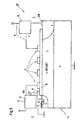
- the poly-silicon resistor could, for example, as a spiral Meander from the high voltage side to the low voltage side or in the form of a zigzag meander.
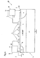
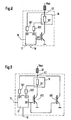
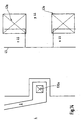
- FIG. 1 shows the plan view of a semiconductor power component 1 according to the invention with a RESURF area 4 arranged between high-voltage side 2 and low-voltage side 3.
- the high-voltage side 2 and the low-voltage side 3 of the power component 1 shown here engage in one another in a finger-shaped manner separated by the RESURF area 4.
- the illustrated power component 1 could be, for example, a diode, a LIGBT, an LDMOS or even a bipolar transistor.
- a poly-silicon resistor 5-here even four poly-silicon resistors 5- is arranged above the RESURF region 4.
- the poly-silicon resistors 5 are guided meander-shaped within the finger structure of the RESURF region 4 from the high-voltage side 2 to the low-voltage side 3.
- the poly-silicon resistors 5 are electrically isolated from the RESURF region 4, which is illustrated by FIGS. 3 to 6.
- the four poly-silicon resistors 5 are propagated at equal intervals one after the other from the high-voltage side 2 and open in the low-voltage side 3. It is advantageous if the poly-silicon resistors 5 have the minimum possible with regard to the manufacturing process Have width and the minimum possible distance from each other or from turn to turn and the high voltage side 2 rotate as often as possible on the basis of the design rules just mentioned.
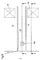
- poly-silicon resistors 5 are each in the form of a zigzag meander whose ends 8 are located on the low-voltage side 3 and whose beginnings 8 * lie on the high-voltage side 2.
- zigzag meandering poly-silicon resistors 5 a signal transfer between the high voltage side 2 and low voltage side 3 is possible.
- the outer corners 6 of the zigzag meanders are respectively connected to poly-silicon strips 7. These poly-silicon strips 7 run on tracks of approximately constant distance from the high-voltage side 2 and the low-voltage side 3, meandering along the RESURF region 4.
- the poly-silicon resistor is designed as a single zigzag meander having two outer ends. These can be completed in the manner described by poly-silicon strips.
- the poly-silicon resistor consists of a parallel connection of the above-described multiple zigzag meanders. The parallel connection is obtained by pairwise connecting the originally adjacent inner ends of the plurality of zigzag meanders.
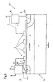
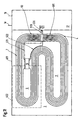
- the lateral pnp transistor 10 shown in cross-section in FIG. 3 has the connections BASE 11, EMITTER 120 and COLLECTOR 13. Such a transistor may comprise any number of fingers and be fabricated on p - substrate, p - / p + substrate or SOI substrate. The variant on p - substrate 14 is shown in detail here. In each of these cases, the RESURF region 4 is then n-doped. The poly-silicon resistor 5 arranged above the RESURF region 4 is electrically insulated from the RESURF region 4 by a field oxide layer 15.
- the poly-silicon resistor 5 is used for signal transmission between a lying at the potential of the high voltage side 2 sensing circuit 16 and a lying on the potential of the low voltage side 3 drive and evaluation circuit 17.
- the poly-silicon resistor 5 is on the High voltage side 2, namely the emitter side, subjected to a voltage signal in the order of the emitter voltage, what it can be connected directly to the external emitter terminal 12 of the sensing circuit 16 alternatively, which is indicated by the wiring b, or with the sensing circuit 16, which by the Wiring a is indicated.
- the low voltage side, ie the collector side, of the poly-silicon resistor 5 is connected via a signal detection input 101 to the drive and evaluation circuit 17.
- the drive and evaluation circuit 17 also has an optional status output 18 and a drive input 19.
- the bipolar transistor 10 shown here can be controlled via the drive input 19 from an external signal source.
- the base terminal 11 can be controlled directly by the drive and evaluation circuit 17.
- the drive and evaluation circuit 17 comprises a drive output 201 with a high-voltage-resistant switching element. This may be, for example, an npn or NMOS transistor whose emitter or source is connected to ground potential and whose collector or drain is connected to the base terminal 11.
- Fig. 4 shows a to Figure 3 analogous cross-sectional view of a lateral diode 20 to the terminals anode 21 and the cathode 220.
- the diode 20 may have any number of fingers and, like the one shown in Figure 3 pnp transistor on p -.. - substrate , p - / p + substrate or on SOI substrate.
- the variant on p - substrate 14 is shown in detail here. In these three cases, the RESURF region 4 always has an n-type doping.
- the poly-silicon resistor 5 is again electrically insulated from the semiconductor substrate 14 by a field oxide layer 15.
- the poly-silicon resistor 5 also serves here again for signal transmission between a sensor circuit 16 located at the potential of the high-voltage side 2 and a drive and evaluation circuit 17 located at the potential of the low-voltage side 3.
- the sensor circuit 16 has an external cathode connection 22 for connection a burden.
- On the high voltage side 2 of the poly-silicon resistor 5 may alternatively be connected directly to this external cathode terminal 22, which is indicated by the wiring b, or with the sensing circuit 16, which is indicated by the wiring a.
- the drive and evaluation circuit 17 has a status input 18 and a signal detection input 101, via which the poly-silicon resistor 5 is connected to the drive and evaluation circuit 17.
- Fig. 5 is a view similar to Figures 3 and 4 cross-sectional view of an LDMOS 30 having the terminals GATE 31, SOURCE 32 and drain 330. Also, such a LDMOS can have as many fingers and how the components previously described on p - - substrate p - / p + - be prepared substrate or SOI substrate. Shown in detail here is the variant on p - - substrate 14.
- An Trust- and Evaluation circuit 17 is electrically insulated by a field oxide layer 15 against the semiconductor substrate 14.
- the drive and evaluation circuit 17 On the high voltage side, it can alternatively be connected directly to the external drain connection 33 (wiring b) or to the sensing circuit 16 (wiring a).
- Low-voltage side of the poly-silicon resistor 5 is connected to a signal detection input 101 of the drive and evaluation circuit 17.
- the drive and evaluation circuit 17 also has an optional status output 18 and a drive input 19, via which the LDMOS 30 can be controlled from an external signal source.
- the drive and evaluation circuit 17 comprises a drive output 201, which is connected to the GATE 31.
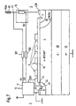
- FIG. 6 shows a cross-section similar to FIGS. 3 to 5 through a LIGBT 40 with the connections GATE 41, ANODE 420 and cathode 43.
- a LIGBT can also have any number of fingers and can be mounted on p - - substrate, p / p + - Substrate or SOI substrate to be produced, wherein the RESURF region 4 always has an n-type doping.
- the variant on p - substrate 14 is shown in detail here.
- the poly-silicon resistor 5 is electrically insulated from the semiconductor substrate 14 by a field oxide layer 15.
- the poly-silicon resistor 5 may alternatively be connected directly to the external anode terminal 42 (line routing b) or to the sensing circuit 16 (FIG. Wiring a) be connected.
- Low-voltage side of the poly-silicon resistor 5 is connected to a signal detection input 101 of the drive and evaluation circuit 17.
- the drive and evaluation circuit 17 also has an optional status output 18 and a Control input 19, via which the LIGBT 40 can be controlled from an external signal source.
- the drive and evaluation circuit 17 comprises a drive output 201, which is connected to the GATE 41, so that the drive and evaluation circuit 17 can selectively act on the GATE 41.
- the sense circuit 16 and the drive and evaluation circuit 17 could be used, for example, to detect and limit the anode voltage of the LIGBT.
- the signal guide b has been selected, so that the sensor circuit 16 can be replaced by a conductive connection.
- To the external anode terminal 42 is connected an inductive load through which a current flows; the LIGBT is on. If the LIGBT is now switched off due to a control signal at the control input 19, for which purpose the drive output 201 of the drive and evaluation circuit 17 reduces its voltage to values below the threshold voltage of the LIGBT, then the voltage at the anode connection 420 or 42 increases. This increase would produce such high anode voltages without further action that the semiconductor device reaches its breakdown voltage.
- the voltage increase at anode terminal 420 or 42 is transmitted via the meandering poly-silicon resistor 5 as a current or voltage signal to the low-voltage side 3 and the signal detection input 101 of the drive and evaluation circuit 17 is supplied.
- the drive and evaluation circuit 17 compares this signal with a reference value, upon reaching the gate 41 is controlled via the drive output 201 such that the anode voltage is limited to a predetermined value.
- LVIGBT lateral-vertical IGBT
- the LVIGBT shown in Fig. 7 is made on a p - / p + substrate but otherwise has the same structure as the LIGBT shown in Fig. 6, so that like reference numerals in Figs. 6 and 7 also denote like elements and circuit components describe.
- the external anode terminal 42 of the LVIGBT is here connected to an inductive load 60, which is fed by an operating voltage source Vbat.
- a sense circuit 16 is used in the embodiment shown here, a resistor 16, which may be implemented, for example in the form of a poly-silicon resistor.
- the drive and evaluation circuit 17 If the drive and evaluation circuit 17 is supplied with a drive voltage via the drive input 19, then the drive output 201 and thus the gate 41 assumes a positive voltage;
- the LVIGBT is turned on: On the surface of the semiconductor under the gate 41, in particular in the p-region 44, an inversion channel is generated, after which electrons are injected from the n-region 45 into the resurf region 4. Thereupon the p-anode 47 responds with a hole injection. As a result, the resurf region 4 and large parts of the p - region 48 are flooded by charge carriers and get into the state of high injection.
- a current of Vbat now flows through the load 60, the resistor 16, via the anode metallization 420, the p-anode 47 and the n-buffer 46.
- a portion of the current flows across the p - region 48 and the p + - Area 49 to the ground on the back of the device from the other part flows through the Resurf region 4 laterally over the p-region 44 and the n-region 45 to the cathode 43, which in turn is connected to ground.
- the current does not immediately reach its static final value, but increases from zero in a slope, which depends on the height of Vbat, the magnitude of the inductance of the load 60 and the voltage drop between the external anode terminal 42 and the cathode 43 of the LVIBGT depends.
- This increase in current causes a current-proportional voltage drop across the resistor 16, which can be determined as explained below.
- the voltage applied to the resistor 16 at the external anode terminal 42 and a designated 301 point is tapped and the signal detection inputs 101 and 102 of the drive and Evaluation circuit 17 supplied.
- the voltage tap is carried out with a respective meander 501 and 502 of the poly-silicon resistor 5.
- the drive and evaluation circuit 17 forms the difference of the signals applied to the signal detection inputs 101 and 102 and thus determines a voltage proportional to the current.
- the voltage thus determined is compared in the drive and evaluation circuit 17 with two reference voltages. If the voltage determined proportional to the current reaches the value of the one reference voltage, then a status signal is generated at the status output 18 of the control and evaluation circuit.
- the drive and evaluation circuit 17 reduces the magnitude of the gate control signal at the drive output 201 to such an extent that a further increase in current through the load 60 is prevented.
- the circuit breaker shown here thus protects itself and the load 60 against overcurrents.
- FIG. 7 shows a circuit diagram of the current-limited LVIGBT just described. The structures bordered by the dashed line are integrated on a chip.
- a small part 402 of the LVIGBT is connected to the load 60 via the resistor 16. This small part 402 is then used as a sense cell. The largest part 401 of the LVIGBT is directly connected to the load 60.
- the advantage of this arrangement over the variant shown in FIG. 8 is a lower voltage drop across the power device, since only part of the load current flows through the resistor 16.
- FIGS. 10 and 11 are schematic plan views showing various possible implementations for the voltage tap across resistor 16 for the LVIGBT shown in FIG.
- the variant shown in FIG. 10 comprises two poly-silicon meanders 501 and 502, which are led directly to the resistor 16.
- the resistor 16 is also made here Poly-silicon.
- the resistor 16 remote from the ends of the poly-silicon meander 501 and 502 are connected via metal leads 510 and 520 to the signal detection inputs 101 and 102 of the drive and evaluation circuit. All other reference numerals correspond to those in Fig. 9.
- the variant shown in Fig. 11 comprises two poly-silicon zigzag meanders 501 and 502, which are guided via metal leads 511 and 522 to the resistor 16.
- the opposite ends of the poly-silicon zigzag meanders 501 and 502 are also connected via metal leads 510 and 520 to the signal detection inputs 101 and 102 of the drive and evaluation circuit. All other reference numerals correspond to those in FIG. 9.
- FIGS. 10 and 11 show a more detailed illustration of the connection guidance of the poly-silicon meanders 501 and 502 to the sense circuit 16 and to the drive and evaluation circuit 17.
- the region around the resistor 16 with the connection points shown in FIG the poly-silicon meander 501 and 502 is shown in Fig. 12 again enlarged in plan view.
- the anode metallizations 420 and 421, which cover the anode diffusions of the two LVIGBT parts 401 and 402 and parts of the resistor 16, are indicated by dashed lines.
- the anode metallization 420 contacts the p-anode diffusion 47 of the LVGBT part 402 in the region 420a and the resistor 16 in the region 420b.
- the anode metallization 421 contacts the p-anode diffusion 471 of the LVGBT part 401 in the region 421a and in the region 421b the Resistor 16.
- the p-type anode diffusions 47 and 471 are each embedded in n-type buffers 46 and 461, respectively.
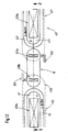
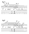
- FIG. 12 illustrates that the poly-silicon meanders 501 and 502 are attached directly to the poly-silicon resistor 16 in the case shown here.
- FIG. 14 shows a plan view of a first realization option without metallization and intermediate dielectric
- FIG. 15 shows a plan view with metallization.
- the end of the poly-silicon meander 5 is contacted by the metal feed line 510 in such a way that it aligns with the cathode metallization 43 on the side facing the high voltage region.
- all sharp corners in the polysilicon are covered by the metallization. Both measures keep field peaks small, which can lead to a reduction of the breakdown voltage of the device.
- 510a designates the region of the metal feed line 510 which contacts the poly-silicon meander 5.
- 43a denotes the regions of the cathode metallization 43 which contact the silicon surface.
- Figures 16 and 17 show cross-sectional images taken along sections CC 'and DD' in Figure 15 without the prior art passivation layers overlying the metallizations.
- the n-type region 45 does not extend over the region over which the metal lead 510 extends, which serves to increase the latch-up strength of the device.
- the intermediate dielectric is designated 80, while the gate oxide is designated 81.
- FIG. 18 shows in plan view a further realization option with metallization and intermediate dielectric.
- the end of the poly-silicon meander 5 is contacted by the metal lead 510 such that it forms an alignment with the cathode metallization 43 on the side facing the high-voltage region.
- all sharp corners in the polysilicon are covered by the metallization. Both measures keep field peaks small, which can lead to a reduction of the breakdown voltage of the device.
- FIGS. 19 and 20 show cross-sectional images along the sections EE 'and FF' in FIG. 18 without the prior art passivation layers lying above the metallizations.
- the n-type region 45 does not extend over the region over which the metal lead 510 extends, which serves to increase the latch-up strength of the device.
- the variant illustrated in FIGS. 18 to 20 will be selected if the end of a poly-silicon meander to be contacted lies at a point which is so unfavorable in the component that the variant described in connection with FIGS. 14 to 17 can not be implemented.
- the contacting of the high-voltage side end of a poly-silicon meander can be carried out accordingly.
Landscapes
- Semiconductor Integrated Circuits (AREA)
- Metal-Oxide And Bipolar Metal-Oxide Semiconductor Integrated Circuits (AREA)
- Insulated Gate Type Field-Effect Transistor (AREA)
- Bipolar Transistors (AREA)
Description
- Die Erfindung betrifft ein Halbleiter-Leistungsbauelement mit einem zwischen Hochspannungsseite und Niederspannungsseite angeordneten REduced SURface Field (RESURF)-Gebiet.
- Bei dem Halbleiter-Leistungsbauelement könnte es sich beispielsweise um eine Diode, einen LIGBT, einen LDMOS oder auch einen Bipolar-Transistor handeln.
- Lateral aufgebaute Leistungsbauelemente umfassen häufig ein RESURF-Gebiet mit einer definierten Dotierungsdosis, die in einem wannenförmigen Verlauf des Feldstärkebetrages an der Halbleiteroberfläche des RESURF-Gebietes und einem über weite Teile linearen Verlauf des Potentials resultiert. Dieser Effekt wird zur Realisierung einer hohen Sperrfähigkeit auf minimaler Chipfläche ausgenutzt. Charakteristischerweise weisen derartige Leistungsbauelemente eine Finger-Interdigitalstruktur auf, so dass die Hochspannungsseite und die Niederspannungsseite fingerförmig ineinandergreifen und durch das die Sperrspannung aufnehmende RESURF-Gebiet voneinander getrennt sind.
- In der Literaturstelle "J.A. Appels et al., IEDM Tech. Dig., 1979 Seiten 238-241" wird das RESURF-Prinzip zum Erreichen einer hohen Sperrspannungsfestigkeit bei geringstem Platzbedarf für flache pn-Übergänge beschrieben.
- In der Literaturstelle "Endo, K. et al., ISPSD '94 Conference Proc., Seiten 379-383" wird ein spiralförmiger Poly-Silizium-Widerstand beschrieben, der als Hochspannungs-Passivierung über dem RESURF-Gebiet einer SOI-Lateral-Diode, eines SOI-LDMOS sowie eines SOI-LIGBT angeordnet ist. Im Falle des LDMOS und des LIGBT ist der Poly-Silizium-Widerstand auf der einen Seite mit der Anode verbunden und auf der anderen Seite mit dem Gate. Im Falle der Diode ist die eine Seite des Poly-Silizium-Widerstandes mit der Anode und die andere Seite mit der Kathode verbunden. In allen drei beschriebenen Fällen dient der Poly-Silizium-Widerstand zur Erhöhung der Hochspannungsfestigkeit flacher pn-Übergänge.
- Beim Einsatz von Leistungsbauelementen der hier in Rede stehenden Art tritt oftmals die Notwendigkeit auf, eine Signalübertragung von der Hochspannungsseite zur Niederspannungsseite zu realisieren. Ein Anwendungsbeispiel für eine solche Signalübertragung stellt die Begrenzung von Überspannungen und Durchlassströmen auf zulässige Maximalwerte dar, die einerseits dem Eigenschutz des Leistungsbauelements dient und andererseits auch dem Schutz seiner peripheren Beschaltung. Die Begrenzung von Überspannungen und Durchlassströmen auf zulässige Maximalwerte wird in der Praxis häufig mit Hilfe von Sense- und Ansteuer- und Auswerteschaltungen realisiert, die vorteilhafterweise auf dem Chip des Leistungsbauelements integriert sein können. So könnte die Stromerfassung durch die Senseschaltung beispielsweise mit Hilfe eines Flächensegments des Leistungsbauelements inklusive Vorwiderstand erfolgen. Das erfasste Stromsignal wird mit Hilfe der Ansteuer- und Auswerteschaltung aufbereitet und ggf. weitergeleitet. Die Ansteuer- und Auswerteschaltung kann dann optional durch eine entsprechende Ansteuerung des Bauelementeneingangs den Strom auf zulässige Werte begrenzen.
- Bei lateralen Leistungsbauelementen besteht oftmals das Problem, dass die Senseschaltung auf dem Potential der Hochspannungsseite liegt und die Ansteuer- und Auswerteschaltung auf dem Potential der Niederspannungsseite liegt, so dass also ein Signaltransfer zwischen der Hochspannungsseite und der Niederspannungsseite des Leistungsbauelements darzustellen ist. Dieser Signaltransfer sollte möglichst flächenneutral sein und die Sperrspannungsfestigkeit des Leistungsbauelements nicht herabsetzen.
- Aus den Druckschriften Patent Abstracts of Japan vol. 2000, no. 04, 31. August 2000 & JE 2000 022175 A (Toshiba Corp), 21. Januar 2000 (2000-01 - 21) &
US 6 150 702 A (Funaki et al.) 21. November 2000 (2000-11-21) und (EP-A-0 576 001 (Tokyo Shibaura Electric Co) 29. Dezember 1993 sind Halbleiter-Leistungsbauelemente bekannt, bei denen zwischen der Hochspannungsseite und der Niederspannungsseite spezielle Gebiete mit verringerter Feldstärke angeordnet sind, diese sind beispielsweise aus Silizium und dienen u.a. zur Spannungsübertragung von der Hochspannungs- auf die Niederspannungsseite. Die Gebiete bilden weiterhin einen Widerstand, der von den übrigen Bereichen des Leistungshalbleiters elektrisch isoliert ist. - Zur Realisierung einer Signalübertragung von der Hochspannungsseite zur Niederspannungsseite eines Halbleiter-Leistungsbauelements der hier in Rede stehenden Art ist erfindungsgemäß mindestens ein Poly-Silizium-Widerstand vorgesehen, der die Hochspannungsseite mit der Niederspannungsseite verbindet. Dieser Poly-Silizium-Widerstand ist über dem RESURF-Gebiet angeordnet und von diesem elektrisch isoliert.
- Erfindungsgemäß ist erkannt worden, dass für eine Signalübertragung von der Hochspannungsseite zur Niederspannungsseite eines Leistungsbauelements ein Element eingesetzt werden sollte, das einen linearen Spannungsabfall entlang seiner Längsausdehnung aufweist, um die optimale Feld- bzw. Potentialverteilung im RESURF-Gebiet nicht zu stören. Es wird daher die Verwendung eines ohmschen Widerstandes vorgeschlagen. Erfindungsgemäß ist ferner erkannt worden, dass im Durchlassfall des Leistungsbauelements hohe Stromdichten und Trägerdichten (Hochinjektion) vorliegen, so dass der Widerstand gegenüber Beeinflussungen infolge dieses Stromflusses isoliert sein muss. Erfindungsgemäß ist schließlich erkannt worden, dass diese Anforderungen sehr gut von einem Poly-Silizium-Widerstand erfüllt werden, der das RESURF-Gebiet überquert und von diesem elektrisch isoliert ist.
- Über den erfindungsgemäß vorgeschlagenen Poly-Silizium-Widerstand ist also gleichzeitig die Übertragung von Messsignalen und im Zusammenspiel mit dem unter ihm angeordneten RESURF-Gebiet die Darstellung einer hohen Sperrspannungsfestigkeit bei minimalem Platzbedarf möglich. Im Gegensatz dazu wäre eine Signalübertragung über einen diffundierten Widerstand im Durchlassfall eines bipolaren Leistungsbauelements unmöglich, da die Signalübertragung durch die üblicherweise vorliegende Hochinjektion gestört würde. Wie bereits erwähnt, ist eine solche Beeinflussung im Falle des erfindungsgemäß vorgeschlagenen Poly-Silizium-Widerstandes ausgeschlossen, da er vollständig vom Halbleiter isoliert ist.
- Um bei hoher Sperrspannung von mehreren Hundert Volt den Leckstrom klein zu halten, muss der Poly-Silizium-Widerstand groß sein, d. h. größer als einige kQ. Er sollte dementsprechend also möglichst lang sein. Diese Länge läßt sich in vorteilhafterweise platzsparend realisieren, indem der Poly-Silizium-Widerstand das RESURF-Gebiet nicht auf dem kürzesten Wege, sondern mäanderförmig überquert. Der Poly-Silizium-Widerstand könnte dazu beispielsweise als spiralförmiger Mäander von der Hochspannungsseite zur Niederspannungsseite geführt sein oder auch in Form eines Zickzack-Mäanders.
- Es erweist sich, den Poly-Silizium-Widerstand durch ein Feldoxid vom RESURF-Gebiet bzw. Halbleiter zu isolieren. Denkbar wäre aber auch der Einsatz von anderen elektrisch isolierenden Materialien.
- Es gibt nun verschiedene Möglichkeiten, die Lehre der vorliegenden Erfindung in vorteilhafter Weise auszugestalten und weiterzubilden. Dazu ist einerseits auf die dem Patentanspruch 1 nachgeordneten Ansprüche und andererseits auf die nachfolgende Erläuterung mehrerer Ausführungsbeispiele der Erfindung anhand der Zeichnungen zu verweisen.
-
- Fig. 1
- zeigt die Draufsicht auf ein erfindungsgemäßes Leistungsbauelement mit RESURF-Gebiet und vier Poly-Silizium-Widerständen.
- Fig. 2
- zeigt die Draufsicht auf ein weiteres erfindungsgemäßes Leistungsbauelement mit zwei zickzack-mäanderförmigen Poly-Silizium-Widerständen.
- Fig. 3
- zeigt einen Querschnitt entlang der in Fig. 1 eingezeichneten Schnittachse AA' für einen lateralen pnp-Transistor.
- Fig. 4
- zeigt einen Querschnitt entlang der in Fig. 1 eingezeichneten Schnittachse AA' für eine laterale Diode.
- Fig. 5
- zeigt einen Querschnitt entlang der in Fig. 1 eingezeichneten Schnittachse AA' für einen LDMOS.
- Fig. 6
- zeigt einen Querschnitt entlang der in Fig. 1 eingezeichneten Schnittachse AA' für einen LIGBT.
- Fig. 7
- zeigt einen der Fig. 6 entsprechenden Querschnitt durch einen Lateral-Vertikal-IGBT (LVIGBT), wobei zusätzlich auch die Verschaltung der Senseschaltung und der Ansteuer- und Auswerteschaltung dargestellt ist.
- Fig. 8
- zeigt die in Fig. 7 dargestellte Situation als Schaltskizze.
- Fig. 9
- zeigt die Schaltskizze eines weiteren LVIGBT mit Senseschaltung und Ansteuer- und Auswerteschaltung.
- Fig. 10
- zeigt die Draufsicht eines Ausführungsbeispiels für den Anschluss von Poly-Silizium-Widerständen an die Senseschaltung und die Ansteuer- und Auswerteschaltung für den in Fig. 9 dargestellten LVIGBT.
- Fig. 11
- zeigt die Draufsicht eines weiteren Ausführungsbeispiels für den Anschluss von Poly-Silizium-Widerständen an die Senseschaltung und die Ansteuer- und Auswerteschaltung für den in Fig. 9 dargestellten LVIGBT.
- Fig. 12
- zeigt eine vergrößerte Draufsicht auf den in Fig.10 dargestellten Bereich des Widerstandes 16.
- Fig. 13
- zeigt einen Querschnitt durch den in Fig. 12 dargestellten Bereich entlang des Schnittes BB'.
- Fig. 14
- zeigt eine Draufsicht auf die Kathodenseite eines LVIGBT ohne Metallisierung und Zwischendielektrikum.
- Fig. 15
- zeigt eine Draufsicht auf die Kathodenseite eines LVIGBT mit Metall.
- Fig. 16
- zeigt einen Querschnitt entlang der in Fig. 15 eingezeichneten Schnittachse CC'.
- Fig. 17
- zeigt einen Querschnitt entlang der in Fig. 15 eingezeichneten Schnittachse DD'.
- Fig. 18
- zeigt eine Draufsicht auf die Kathodenseite eines LVIGBT mit Metallisierung und Zwischendielektrikum.
- Fig. 19
- zeigt einen Querschnitt entlang der in Fig. 18 eingezeichneten Schnittachse EE'.
- Fig. 20
- zeigt einen Querschnitt entlang der in Fig. 18 eingezeichneten Schnittachse FF'.
- Wie bereits erwähnt, ist in Fig. 1 die Draufsicht auf ein erfindungsgemäßes Halbleiter-Leistungsbauelement 1 dargestellt mit einem zwischen Hochspannungsseite 2 und Niederspannungsseite 3 angeordneten RESURF-Gebiet 4. Die Hochspannungsseite 2 und die Niederspannungsseite 3 des hier dargestellten Leistungsbauelements 1 greifen fingerförmig ineinander und sind durch das RESURF-Gebiet 4 voneinander getrennt. An dieser Stelle sei noch angemerkt, dass es sich bei dem dargestellten Leistungsbauelement 1 beispielsweise um eine Diode, einen LIGBT, einen LDMOS oder auch um einen Bipolar-Transistor handeln könnte.
- Erfindungsgemäß ist ein Poly-Silizium-Widerstand 5 - hier sogar vier Poly-Silizium-Widerstände 5 - über dem RESURF-Gebiet 4 angeordnet. Im hier dargestellten Ausführungsbeispiel sind die Poly-Silizium-Widerstände 5 mäanderförmig innerhalb der Fingerstruktur des RESURF-Gebiets 4 von der Hochspannungsseite 2 zur Niederspannungsseite 3 geführt. Die Poly-Silizium-Widerstände 5 sind von dem RESURF-Gebiet 4 elektrisch isoliert, was durch die Figuren 3 bis 6 verdeutlicht wird.
- Im hier dargestellten Ausführungsbeispiel gehen die vier Poly-Silizium-Widerstände 5 in gleichen Abständen nacheinander von der Hochspannungsseite 2 aus und münden in der Niederspannungsseite 3. Von Vorteil ist es, wenn die Poly-Silizium-Widerstände 5 die im Hinblick auf den Herstellungsprozess minimal mögliche Breite und den minimal möglichen Abstand voneinander bzw. von Windung zu Windung aufweisen und die Hochspannungsseite 2 so oft umlaufen, wie es auf der Basis der eben genannten Designregeln möglich ist.
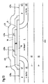
- Eine weitere Möglichkeit der Anordnung von Poly-Silizium-Widerständen 5 auf dem RESURF-Gebiet 4 eines Leistungsbauelements 1 ist in Fig. 2 dargestellt. Hier sind zwei Poly-Silizium-Widerstände 5 jeweils in Form eines Zickzack-Mäanders ausgeführt, deren Enden 8 sich auf der Niederspannungsseite 3 befinden und deren Anfänge 8* auf der Hochspannungsseite 2 liegen. Über diese zickzack-mäanderförmigen Poly-Silizium-Widerstände 5 ist ein Signaltransfer zwischen Hochspannungsseite 2 und Niederspannungsseite 3 möglich. Zum Erzielen einer hohen Sperrfähigkeit werden die äußeren Ecken 6 der Zickzack-Mäander jeweils an Poly-Silizium-Streifen 7 angeschlossen. Diese Poly-Silizium-Streifen 7 verlaufen auf Bahnen mit ungefähr konstantem Abstand von der Hochspannungsseite 2 bzw. der Niederspannungsseite 3, mäanderförmig entlang des RESURF-Gebietes 4. Durch diese Ausgestaltung werden Spitzen der elektrischen Feldstärke bzw. Feldüberhöhungen im Halbleiter unter den äußeren Ecken 6 der zickzack-mäanderförmigen Poly-Silizium-Widerstände 5 vermieden. Auf diese Weise wird einem Avalanche-Durchbruch des Bauelements schon bei kleinen Spannungen und damit einer Herabsetzung der Sperrfähigkeit vorgebeugt. Außerdem wird mit Hilfe der Poly-Silizium-Streifen 7 der Potentialverlauf über dem RESURF-Gebiet 4 stabilisiert, was auch zu einer Stabilitätserhöhung des Bauelements unter hoher Sperrspannung führt.
- Feldüberhöhungen im Halbleiter unter den inneren Enden 8 der zickzack-mäanderförmigen Poly-Silizium-Widerstände 5 werden im vorliegenden Ausführungsbeispiel dadurch minimiert, dass diese inneren Enden 8 möglichst nahe zueinander angeordnet sind.
- Für den Fall, dass nur ein einzelner Poly-Silizium-Widerstand benötigt wird, kommen prinzipiell zwei Ausgestaltungsmöglichkeiten in Fragen. In der ersten Variante wird der Poly-Silizium-Widerstand als einzelner Zickzack-Mäander ausgeführt, der zwei äußere Enden aufweist. Diese lassen sich in der beschriebenen Weise durch Poly-Silizium-Streifen abschließen. In der zweiten Variante besteht der Poly-Silizium-Widerstand aus einer Parallelschaltung der oben beschriebenen mehreren Zickzack-Mäander. Die Parallelschaltung erhält man durch jeweils paarweises Verbinden der ursprünglich benachbarten inneren Enden der mehreren Zickzack-Mäander.
- Die in Verbindung mit Fig. 2 vorgeschlagenen Ausgestaltungen der erfindungsgemäßen Poly-Silizium-Widerstände haben gegenüber den in Verbindung mit Fig. 1 vorgeschlagenen Formen den Vorteil einer einfachen, d.h. zeitsparenden, Umsetzung im Layout. Demgegenüber lassen sich mit den in Verbindung mit Fig. 1 beschriebenen Ausgestaltungen höherohmige Widerstände realisieren.
- Der in Fig. 3 im Querschnitt dargestellte laterale pnp-Transistor 10 weist die Anschlüsse BASIS 11, EMITTER 120 und KOLLEKTOR 13 auf. Ein derartiger Transistor kann beliebig viele Finger umfassen und auf p- - Substrat, p- / p+ - Substrat oder SOI-Substrat hergestellt sein. Im Detail dargestellt ist hier die Variante auf p-- Substrat 14. In jedem dieser Fälle ist das RESURF-Gebiet 4 dann n-dotiert. Der über dem RESURF-Gebiet 4 angeordnete Poly-Silizium-Widerstand 5 ist durch eine Feldoxidschicht 15 gegen das RESURF-Gebiet 4 elektrisch isoliert.
- Im hier dargestellten Ausführungsbeispiel dient der Poly-Silizium-Widerstand 5 zur Signalübertragung zwischen einer auf dem Potential der Hochspannungsseite 2 liegenden Senseschaltung 16 und einer auf dem Potential der Niederspannungsseite 3 liegenden Ansteuer- und Auswerteschaltung 17. Der Poly-Silizium-Widerstand 5 wird auf der Hochspannungsseite 2, nämlich der Emitterseite, mit einem Spannungssignal in der Größenordnung der Emitterspannung beaufschlagt, wozu er alternativ direkt mit dem externen Emitteranschluß 12 der Senseschaltung 16 verbunden werden kann, was durch die Leitungsführung b angedeutet ist, oder mit der Senseschaltung 16, was durch die Leitungsführung a angedeutet ist. Die Niederspannungsseite, d. h. die kollektornahe Seite, des Poly-Silizium-Widerstandes 5 ist über einen Signalerfassungseingang 101 mit der Ansteuer- und Auswerteschaltung 17 verbunden.
- Die Ansteuer- und Auswerteschaltung 17 weist ferner einen optionalen Statusausgang 18 und einen Ansteuereingang 19 auf. Der hier dargestellte Bipolartransistor 10 läßt sich über den Ansteuereingang 19 von einer externen Signalquelle ansteuern. Der Basisanschluss 11 kann direkt von der Ansteuer- und Auswerteschaltung 17 angesteuert werden. Dazu umfasst die Ansteuer- und Auswerteschaltung 17 einen Ansteuerausgang 201 mit einem hochspannungsfesten Schaltelement. Dabei kann es sich beispielsweise um einen npn- bzw. NMOS-Transistor handeln, dessen Emitter bzw. Source mit Massepotential und dessen Kollektor bzw. Drain mit dem Basisanschluss 11 verbunden ist.
- Fig. 4 zeigt einen zu Fig. 3 analogen Querschnitt durch eine laterale Diode 20 mit den Anschlüssen ANODE 21 und KATHODE 220. Die Diode 20 kann beliebig viele Finger aufweisen und genau wie der in Fig. 3 dargestellte pnp-Transistor auf p-- Substrat, p-/p+- Substrat oder auf SOI-Substrat hergestellt sein. Im Detail dargestellt ist hier die Variante auf p- - Substrat 14. In diesen drei Fällen weist das RESURF-Gebiet 4 immer eine n-Dotierung auf. Der Poly-Silizium-Widerstand 5 ist wieder durch eine Feldoxidschicht 15 gegen das Halbleitersubstrat 14 elektrisch isoliert. Außerdem dient der Poly-Silizium-Widerstand 5 auch hier wieder zur Signalübertragung zwischen einer auf dem Potential der Hochspannungsseite 2 liegenden Senseschaltung 16 und einer auf dem Potential der Niederspannungsseite 3 liegenden Ansteuer- und Auswerteschaltung 17. Die Senseschaltung 16 weist einen externen Kathodenanschluss 22 zum Anschluss einer Last auf. Auf der Hochspannungsseite 2 kann der Poly-Silizium-Widerstand 5 alternativ direkt mit diesem externen Kathodenanschluss 22 verbunden sein, was durch die Leitungsführung b angedeutet ist, oder mit der Senseschaltung 16, was durch die Leitungsführung a angedeutet ist. Die Ansteuer- und Auswerteschaltung 17 weist einen Statuseingang 18 auf und einen Signalerfassungseingang 101, über den der Poly-Silizium-Widerstand 5 an die Ansteuer- und Auswerteschaltung 17 angeschlossen ist.
- Fig. 5 zeigt eine zu den Figuren 3 und 4 analoge Querschnittsdarstellung eines LDMOS 30 mit den Anschlüssen GATE 31, SOURCE 32 und DRAIN 330. Auch ein derartiger LDMOS kann beliebig viele Finger aufweisen und wie die voranstehend beschriebenen Bauelemente auf p- - Substrat, p-/p+ - Substrat oder SOI-Substrat hergestellt sein. Im Detail dargestellt ist hier die Variante auf p- - Substrat 14. Der Poly-Silizium-Widerstand 5, der auch hier zur Signalübertragung zwischen einer auf dem Potential der Hochspannungsseite 2 liegenden Senseschaltung 16 und einer auf dem Potential der Niederspannungsseite 3 liegenden Ansteuer- und Auswerteschaltung 17 dient, ist durch eine Feldoxidschicht 15 gegen das Halbleitersubstrat 14 elektrisch isoliert. Er kann hochspannungsseitig alternativ direkt mit dem externen Drainanschluss 33 (Leitungsführung b) oder mit der Senseschaltung 16 (Leitungsführung a) verbunden sein. Niederspannungsseitig ist der Poly-Silizium-Widerstand 5 an einen Signalerfassungseingang 101 der Ansteuer- und Auswerteschaltung 17 angeschlossen. Die Ansteuer- und Auswerteschaltung 17 weist außerdem einen optionalen Statusausgang 18 und einen Ansteuereingang 19 auf, über den der LDMOS 30 von einer externen Signalquelle aus ansteuerbar ist. Dazu umfasst die Ansteuer- und Auswerteschaltung 17 einen Ansteuerausgang 201, der mit dem GATE 31 verbunden ist.
- Fig. 6 zeigt einen zu den Figuren 3 bis 5 analogen Querschnitt durch einen LIGBT 40 mit den Anschlüssen GATE 41, ANODE 420 und Kathode 43. Auch ein solcher LIGBT kann beliebig viele Finger aufweisen und auf p- - Substrat, p/p+ - Substrat oder SOI-Substrat hergestellt sein, wobei das RESURF-Gebiet 4 immer eine n-Dotierung aufweist. Im Detail dargestellt ist hier die Variante auf p- - Substrat 14. Wieder ist der Poly-Silizium-Widerstand 5 durch eine Feldoxidschicht 15 gegen das Halbleitersubstrat 14 elektrisch isoliert. Er dient auch hier zur Signalübertragung zwischen einer hochspannungsseitig angeordneten Senseschaltung 16 und einer niederspannungsseitig angeordneten Ansteuer- und Auswerteschaltung 17. Im vorliegenden Ausführungsbeispiel kann der Poly-Silizium-Widerstand 5 alternativ direkt mit dem externen Anodenanschluss 42 (Leitungsführung b) oder mit der Senseschaltung 16 (Leitungsführung a) verbunden sein. Niederspannungsseitig ist der Poly-Silizium-Widerstand 5 an einen Signalerfassungseingang 101 der Ansteuer- und Auswerteschaltung 17 angeschlossen. Die Ansteuer- und Auswerteschaltung 17 weist außerdem einen optionalen Statusausgang 18 und einen Ansteuereingang 19 auf, über den der LIGBT 40 von einer externen Signalquelle aus ansteuerbar ist. Dazu umfasst die Ansteuer- und Auswerteschaltung 17 einen Ansteuerausgang 201, der mit dem GATE 41 verbunden ist, so dass die Ansteuer- und Auswerteschaltung 17 wahlweise regelnd auf das GATE 41 einwirken kann.
- Selbstverständlich sind alle in Verbindung mit den Figuren 3 bis 6 erwähnten Dotierungen vertauschbar - p gegen n -, wobei die gezeichneten Anschlüsse und Potentiale dann sinngemäß zu ändern sind.
- Die Senseschaltung 16 und die Ansteuer- und Auswerteschaltung 17 könnten beispielsweise zur Erfassung und Begrenzung der Anodenspannung des LIGBT eingesetzt werden. Für die nachfolgende Erläuterung ist die Signalführung b gewählt worden, so dass die Senseschaltung 16 durch eine leitende Verbindung ersetzt werden kann. An den externen Anodenanschluss 42 sei eine induktive Last angeschlossen, durch die ein Strom fließt; der LIGBT sei eingeschaltet. Wird der LIGBT nun aufgrund eines Steuersignals am Ansteuereingang 19 ausgeschaltet, wozu der Ansteuerausgang 201 der Ansteuer- und Auswerteschaltung 17 seine Spannung auf Werte unterhalb der Schwellspannung des LIGBTs reduziert, so steigt die Spannung am Anodenanschluss 420 bzw. 42 an. Dieser Anstieg würde ohne weitere Maßnahmen so hohe Anodenspannungen erzeugen, dass das Halbleiterbauelement seine Durchbruchspannung erreicht.
- Um einen unkontrollierten Anstieg der Anodenspannung zu verhindern, wird der Spannungsanstieg am Anodenanschluss 420 bzw. 42 über den mäanderförmigen Poly-Silizium-Widerstand 5 als Strom- oder Spannungssignal auf die Niederspannungsseite 3 übertragen und dem Signalerfassungseingang 101 der Ansteuer- und Auswerteschaltung 17 zugeführt. Die Ansteuer- und Auswerteschaltung 17 vergleicht dieses Signal mit einem Referenzwert, bei dessen Erreichen das Gate 41 über den Ansteuerausgang 201 derart ausgesteuert wird, dass die Anodenspannung auf einen vorgegebenen Wert begrenzt wird.
- In Verbindung mit den Figuren 7 und 8 wird nachfolgend ein Lateral-Vertikal-IGBT (LVIGBT) mit Strombegrenzung und Stromstatusausgabe beschrieben, um ein weiteres Ausführungsbeispiel für eine Senseschaltung und eine Ansteuer- und Auswerteschaltung zu geben.
- Der in Fig. 7 dargestellte LVIGBT ist auf einem p- / p+ - Substrat hergestellt weist aber ansonsten den gleichen Aufbau auf, wie der in Fig. 6 dargestellte LIGBT, so dass gleiche Bezugszeichen in den Figuren 6 und 7 auch gleiche Elemente und Schaltungskomponenten bezeichnen. Der externe Anodenanschluss 42 des LVIGBT ist hier mit einer induktiven Last 60 verbunden, die über eine Betriebsspannungsquelle Vbat gespeist wird. Als Senseschaltung 16 dient im hier dargestellten Ausführungsbeispiel ein Widerstand 16, der z.B. in Form eines Poly-Silizium-Widerstandes realisiert sein kann. Wird der Ansteuer- und Auswerteschaltung 17 über den Ansteuereingang 19 eine Ansteuerspannung zugeführt, dann nimmt der Ansteuerausgang 201 und damit Gate 41 eine positive Spannung an; der LVIGBT wird eingeschaltet: An der Oberfläche des Halbleiters unter dem Gate 41, insbesondere im p-Gebiet 44 wird ein Inversionskanal erzeugt, woraufhin Elektronen vom n-Gebiet 45 in das Resurf-Gebiet 4 injiziert werden. Darauf antwortet die p-Anode 47 mit einer Löcherinjektion. In der Folge werden das Resurf-Gebiet 4 und große Teile des p--Gebietes 48 von Ladungsträgern überschwemmt und geraten in den Zustand der Hochinjektion. Es fließt jetzt ein Strom von Vbat durch die Last 60, den Widerstand 16, über die Anodenmetallisierung 420, die p-Anode 47 und den n-Buffer 46. Ein Teil des Stromes fließt über das p--Gebiet 48 und das p+-Gebiet 49 zur Masse auf der Rückseite des Bauelements ab, der andere Teil fließt über das Resurf-Gebiet 4 lateral über das p-Gebiet 44 und das n-Gebiet 45 zur Kathode 43, die ihrerseits mit Masse verbunden ist. Infolge der induktiven Last 60 erreicht der Strom nicht sofort seinen statischen Endwert, sondern steigt von Null in einer Steilheit an, die von der Höhe von Vbat, der Größe der Induktivität der Last 60 und dem Spannungsabfall zwischen dem externen Anodenanschluss 42 und der Kathode 43 des LVIBGT abhängt. Dieser Stromanstieg verursacht einen dem Strom proportionalen Spannungsabfall über dem Widerstand 16, der sich wie nachfolgend erläutert ermitteln läßt.
- Wie in den Figuren 7 und 8 gezeigt, wird die am Widerstand 16 anliegende Spannung am externen Anodenanschluss 42 und einer mit 301 bezeichneten Stelle abgegriffen und den Signalerfassungseingängen 101 und 102 der Ansteuer- und Auswerteschaltung 17 zugeführt. Der Spannungsabgriff erfolgt mit je einem Mäander 501 und 502 des Poly-Silizium-Widerstandes 5. Die Ansteuer- und Auswerteschaltung 17 bildet die Differenz der an den Signalerfassungseingängen 101 und 102 anliegende Signale und ermittelt somit eine dem Strom proportionale Spannung. Die so ermittelte Spannung wird in der Ansteuer- und Auswerteschaltung 17 mit zwei Referenzspannungen verglichen. Erreicht die dem Strom proportionale ermittelte Spannung den Wert der einen Referenzspannung, so wird am Statusausgang 18 der Ansteuer- und Auswerteschaltung ein Statussignal erzeugt. Erreicht die ermittelte Spannung den Wert der anderen Referenzspannung, so reduziert die Ansteuer- und Auswerteschaltung 17 den Betrag des Gatesteuersignals am Ansteuerausgang 201 soweit, dass ein weiterer Stromanstieg durch die Last 60 verhindert wird. Der hier dargestellte Leistungsschalter schützt somit sich selbst und die Last 60 vor Überströmen.
- In Fig. 7 sind die beiden Mäander 501 und 502 des Poly-Silizium-Widerstandes 5 in ihrer elektrischen Verschaltung als 501 und 502 dargestellt. Im Querschnittsbild des LVIGBT sind sie ferner in ihrer prinzipiellen Lage angedeutet und als 5 gekennzeichnet. In Fig. 8 ist eine Schaltskizze des eben beschriebenen LVIGBT mit Strombegrenzung dargestellt. Die mit der gestrichelten Linie umrandeten Strukturen sind auf einem Chip integriert.
- In einer vorteilhaften Ausführungsform, die als Schaltskizze in Fig. 9 dargestellt ist, ist lediglich ein kleiner Teil 402 des LVIGBT über den Widerstand 16 mit der Last 60 verbunden. Dieser kleine Teil 402 wird dann quasi als Sensezelle verwendet. Der größte Teil 401 des LVIGBT ist direkt mit der Last 60 verbunden. Der Vorteil dieser Anordnung gegenüber der in Fig. 8 dargestellten Variante ist ein geringerer Spannungsabfall über dem Leistungsbauelement, da nur ein Teil des Laststromes durch den Widerstand 16 fließt.
- Bei den Figuren 10 und 11 handelt es sich um schematische Draufsichten, die verschiedene Realisierungsmöglichkeiten für den Spannungsabgriff über dem Widerstand 16 für den in Fig. 9 dargestellten LVIGBT zeigen. Die in Fig. 10 dargestellte Variante umfasst zwei Poly-Silizium-Mäander 501 und 502, die direkt an den Widerstand 16 geführt sind. Der Widerstand 16 besteht hier ebenfalls aus Poly-Silizium. Die dem Widerstand 16 abgewandten Enden der Poly-Silizium-Mäander 501 und 502 sind über Metallzuleitungen 510 und 520 an die Signalerfassungseingänge 101 und 102 der Ansteuer- und Auswerteschaltung angeschlossen. Alle anderen Bezugszeichen entsprechen denen in Fig. 9. Die in Fig. 11 dargestellte Variante umfasst zwei Poly-Silizium-Zickzack-Mäander 501 und 502, die über Metallzuleitungen 511 und 522 an den Widerstand 16 geführt sind. Die dem Widerstand 16 abgewandten Enden der Poly-Silizium-Zickzack-Mäander 501 und 502 sind ebenfalls über Metallzuleitungen 510 und 520 an die Signalerfassungseingänge 101 und 102 der Ansteuer- und Auswerteschaltung angeschlossen. Alle anderen Bezugszeichen entsprechen denen in Fig. 9.
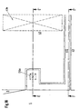
- Wie bereits erwähnt zeigen die Figuren 10 und 11 eine genauere Darstellung der Anschlussführung der Poly-Silizium-Mäander 501 und 502 an die Senseschaltung 16 und an die Ansteuer- und Auswerteschaltung 17. Der in Fig. 10 dargestellte Bereich um den Widerstand 16 mit den Anschlussstellen der Poly-Silizium-Mäander 501 und 502 ist in Fig. 12 nochmals vergrößert in Draufsicht dargestellt.
- Die Anodenmetallisierungen 420 und 421, die die Anodendiffusionen der beiden LVIGBT-Teile 401 und 402 und Teile des Widerstandes 16 überdecken, sind gestrichelt angedeutet. Die Anodenmetallisierung 420 kontaktiert im Bereich 420a die p-Anodendiffusion 47 des LVGBT-Teils 402 und im Bereich 420b den Widerstand 16. Entsprechend kontaktiert die Anodenmetallisierung 421 im Bereich 421 a die p-Anodendiffusion 471 des LVGBT-Teils 401 und im Bereich 421 b den Widerstand 16. Die p-Anodendiffusionen 47 und 471 sind jeweils in einen n-Buffer 46 bzw. 461 eingebettet. Eine die Poly-Silizium-Mäander 501 und 502 gegen das RESURF-Gebiet elektrisch isolierende Feldoxidschicht und eine die Metallisierungen und das Poly-Silizium voneinander isolierende Zwischenoxidschicht sind aus Gründen der Übersichtlichkeit zwar nicht in Fig. 12 dargestellt, aber in Fig.13, die einen Querschnitt entlang des Schnittes BB' in Fig. 12 wiedergibt. Weder in Fig. 12 noch in Fig 13 sind die nach dem Stand der Technik üblichen, über den Metallisierungen liegenden Passivierungsschichten dargestellt. Fig. 12 verdeutlicht, dass die Poly-Silizium-Mäander 501 und 502 im hier dargestellten Fall direkt an den Poly-Silizium-Widerstand 16 angesetzt sind.
- An den Stellen, an denen ein über dem Resurf-Gebiet 4 angeordneter Poly-Silizium-Mäander endet und die Signalweiterführung mittels Metallzuleitungen durchgeführt wird, ist eine besondere Konstruktion nötig, um die Sperrfähigkeit des Bauelements nicht deutlich zu reduzieren.
- Am Beispiel der Kathodenseite des in Fig. 7 dargestellten LVIGBT werden nachfolgend zwei Ausführungsbeispiele für derartige Konstruktionen erläutert.
- In Fig. 14 ist in Draufsicht eine erste Realisierungsmöglichkeit ohne Metallisierung und Zwischendielektrikum dargestellt; eine Draufsicht mit Metallisierung zeigt Fig. 15. Das Ende des Poly-Silizium-Mäanders 5 wird so von der Metallzuleitung 510 kontaktiert, dass diese auf der dem Hochspannungsgebiet zugewandten Seite eine Flucht mit der Kathodenmetallisierung 43 bildet; außerdem werden alle spitzen Ecken im Polysilizium von der Metallisierung verdeckt. Beide Maßnahmen halten Feldspitzen klein, die zu einer Reduktion der Durchbruchspannung des Bauelements führen können. Mit 510a ist der Bereich der Metallzuleitung 510 bezeichnet, der den Poly-Silizium-Mäander 5 kontaktiert. Mit 43a sind die Bereiche der Kathodenmetallisierung 43 bezeichnet, die die Silizium-Oberfläche kontaktieren.
- Die Figuren 16 und 17 zeigen Querschnittsbilder entlang der Schnitte CC' und DD' in Fig. 15 ohne die nach dem Stand der Technik üblichen, über den Metallisierungen liegenden Passivierungsschichten. Das n-Gebiet 45 erstreckt sich nicht über den Bereich, über den die Metallzuleitung 510 verläuft, was der Erhöhung der Latch-up-Festigkeit des Bauelements dient. Das Zwischendielektrikum ist mit 80 bezeichnet, während das Gateoxid mit 81 bezeichnet ist.
- In Fig. 18 ist in Draufsicht eine weitere Realisierungsmöglichkeit mit Metallisierung und Zwischendielektrikum dargestellt. Das Ende des Poly-Silizium-Mäanders 5 wird so von der Metallzuleitung 510 kontaktiert, dass diese auf der dem Hochspannungsgebiet zugewandten Seite eine Flucht mit der Kathodenmetallisierung 43 bildet. Außerdem werden alle spitzen Ecken im Polysilizium von der Metallisierung verdeckt. Beide Maßnahmen halten Feldspitzen klein, die zu einer Reduktion der Durchbruchspannung des Bauelements führen können.
- Die Figuren 19 und 20 zeigen Querschnittsbilder entlang der Schnitte EE' und FF' in Fig. 18 ohne die nach dem Stand der Technik üblichen, über den Metallisierungen liegenden Passivierungsschichten. Das n-Gebiet 45 erstreckt sich nicht über den Bereich, über den die Metallzuleitung 510 verläuft, was der Erhöhung der Latch-up-Festigkeit des Bauelements dient.
- Die in den Figuren 18 bis 20 dargestellte Variante wird man wählen, wenn das zu kontaktierende Ende eines Poly-Silizium-Mäanders an einer im Bauelement so ungünstigen Stelle liegt, dass die in Verbindung mit den Figuren 14 bis 17 beschriebene Variante nicht umsetzbar ist.
- Die Kontaktierung des hochspannungsseitigen Endes eines Poly-Silizium-Mäanders läßt sich entsprechend auszuführen.
Claims (10)
- Halbleiter-Leistungsbauelement (1) mit einem zwischen Hochspannungsseite (2) und Niederspannungsseite (3) angeordneten Reduced SURface Field, RESURF-Gebiet (4), wobei mindestens ein Poly-Silizium (Si)-Widerstand (5) zur Signalübertragung zwischen Hochspannungsseite (2) und Niederspannungsseite (3) vorgesehen ist, dass der Poly-Si-Widerstand (5) über dem RESURF-Gebiet (4) angeordnet ist und dass der Poly-Si-Widerstand (5) von dem RESURF-Gebiet (4) elektrisch isoliert ist, dadurch gekennzeichnet, dass der Poly-Si-Widerstand (5) zumindest durch eine Feldoxidschicht (15) von dem RESURF-Gebiet (4) elektrisch isoliert ist und mindestens eine Senseschaltung (16) und mindestens eine Ansteuer- und Auswerteschaltung (17) zur Begrenzung von Überspannungen oder Durchlassströmen auf zulässige Maximalwerte vorgesehen ist und die Senseschaltung (16) auf dem Potential der Hochspannungsseite (2) liegt und die Ansteuer- und Auswerteschaltung (17) auf dem Potential der Niederspannungsseite (3) liegt.
- Halbleiter-Leistungsbauelement (1) nach Anspruch 1, dadurch gekennzeichnet, dass der Poly-Si-Widerstand (5) mäanderförmig von der Hochspannungsseite (2) zur Niederspannungsseite (3) geführt ist
- Halbleiter-Leistungsbauelement (1) nach einem der Ansprüche 1 oder 2, dadurch gekennzeichnet, dass der Poly-Si-Widerstand (5) als spiralförmiger Mäander von der Hochspannungsseite (2) zur Niederspannungsseite (3) geführt ist.
- Halbleiter-Leistungsbauelement (1) nach einem der Ansprüche 1 oder 2, dadurch gekennzeichnet, dass der Poly-Si-Widerstand (5) in Form eines Zickzack-Mäanders von der Hochspannungsseite (2) zur Niederspannungsseite (3) geführt ist.
- Halbleiter-Leistungsbauelement (1) nach einem der vorhergehenden Ansprüche dadurch gekennzeichnet, dass der Poly-Si-Widerstand (5) zur Signalübertragung zwischen Senseschaltung (16) und Ansteuer- und Auswerteschaltung (17) dient.
- Halbleiter-Leistungsbauelement (1) nach Anspruch 5, dadurch gekennzeichnet, dass die Senseschaltung (16) und/oder die Ansteuer- und Auswerteschaltung (17) auf demselben Chip integriert sind wie das Leistungsbauelement (1).
- Halbleiter-Diode 20) nach einem der Ansprüche 1 bis 6, dadurch gekennzeichnet, dass der Poly-Si-Widerstand (5) zur Signalübertragung zwischen Kathode (22) und Anode (21) dient.
- Halbleiter-LIGBT (40) nach einem der Ansprüche 1 bis 6, dadurch gekennzeichnet, dass der Poly-Si-Widerstand (5) zur Signalübertragung zwischen Kathode (43) und Anode (42) dient.
- Halbleiter-LDMOS (30) nach einem der Ansprüche 1 bis 6, dadurch gekennzeichnet, dass der Poly-Si-Widerstand (5) zur Signalübertragung zwischen Drain (33) und Source (32) dient.
- Halbleiter-Bipolar-Transistor (10) nach einem der Ansprüche 1 bis 6, dadurch gekennzeichnet, dass der Poly-Si-Widerstand (5) zur Signalübertragung zwischen Emitter (12)und Kollektor (13) dient.
Applications Claiming Priority (3)
| Application Number | Priority Date | Filing Date | Title |
|---|---|---|---|
| DE10023956A DE10023956A1 (de) | 2000-05-16 | 2000-05-16 | Halbleiter-Leistungsbauelement |
| DE10023956 | 2000-05-16 | ||
| PCT/DE2001/001774 WO2001088992A2 (de) | 2000-05-16 | 2001-05-10 | Halbleiter-leistungsbauelement |
Publications (2)
| Publication Number | Publication Date |
|---|---|
| EP1284019A2 EP1284019A2 (de) | 2003-02-19 |
| EP1284019B1 true EP1284019B1 (de) | 2007-09-26 |
Family
ID=7642253
Family Applications (1)
| Application Number | Title | Priority Date | Filing Date |
|---|---|---|---|
| EP01940224A Expired - Lifetime EP1284019B1 (de) | 2000-05-16 | 2001-05-10 | Halbleiter-leistungsbauelement |
Country Status (7)
| Country | Link |
|---|---|
| US (1) | US20040046225A1 (de) |
| EP (1) | EP1284019B1 (de) |
| JP (1) | JP2003533886A (de) |
| KR (1) | KR100844283B1 (de) |
| CZ (1) | CZ302020B6 (de) |
| DE (2) | DE10023956A1 (de) |
| WO (1) | WO2001088992A2 (de) |
Families Citing this family (12)
| Publication number | Priority date | Publication date | Assignee | Title |
|---|---|---|---|---|
| GB2387481B (en) | 2002-04-10 | 2005-08-31 | Intense Photonics Ltd | Integrated active photonic device and photodetector |
| DE102005037409A1 (de) | 2004-08-09 | 2006-03-30 | International Rectifier Corp., El Segundo | Start-Up Schalter um einer Anwendungsschaltung eine Start-Up Spannung zur Verfügung zu stellen |
| JP4797203B2 (ja) | 2008-12-17 | 2011-10-19 | 三菱電機株式会社 | 半導体装置 |
| JP2013120815A (ja) * | 2011-12-07 | 2013-06-17 | Sony Corp | Esd保護回路およびこれを備えた半導体装置 |
| JP6597269B2 (ja) | 2015-12-15 | 2019-10-30 | 富士電機株式会社 | 半導体装置 |
| US10396167B2 (en) | 2015-12-15 | 2019-08-27 | Fuji Electric Co., Ltd. | Semiconductor device |
| JP6690336B2 (ja) | 2016-03-18 | 2020-04-28 | 富士電機株式会社 | 半導体装置 |
| EP3327756B1 (de) * | 2016-11-24 | 2019-11-06 | Melexis Technologies NV | System zur überwachung der integrität des rands eines dies und zugehöriges verfahren |
| DE102017130213B4 (de) * | 2017-12-15 | 2021-10-21 | Infineon Technologies Ag | Planarer feldeffekttransistor |
| DE102019119805B4 (de) * | 2018-09-28 | 2024-09-26 | Taiwan Semiconductor Manufacturing Co., Ltd. | Halbleitervorrichtung, die einen kondensator aufweist, sowie verfahren zu ihrer herstellung |
| US11152356B2 (en) * | 2019-02-19 | 2021-10-19 | Semiconductor Components Industries, Llc | Method of forming a semiconductor device and structure therefor |
| CN113948571B (zh) * | 2021-10-18 | 2023-08-25 | 上海华虹宏力半导体制造有限公司 | 半导体结构及其形成方法 |
Family Cites Families (14)
| Publication number | Priority date | Publication date | Assignee | Title |
|---|---|---|---|---|
| US4157563A (en) * | 1971-07-02 | 1979-06-05 | U.S. Philips Corporation | Semiconductor device |
| NL187415C (nl) * | 1980-09-08 | 1991-09-16 | Philips Nv | Halfgeleiderinrichting met gereduceerde oppervlakteveldsterkte. |
| JPH04245483A (ja) * | 1991-01-30 | 1992-09-02 | Nippondenso Co Ltd | 半導体装置 |
| JPH05121418A (ja) * | 1991-10-24 | 1993-05-18 | Nec Corp | 半導体装置 |
| JP3207615B2 (ja) * | 1992-06-24 | 2001-09-10 | 株式会社東芝 | 半導体装置 |
| KR0127003Y1 (ko) * | 1992-06-24 | 1998-12-01 | 사또 후미오 | 전력 반도체 집적 회로 장치 |
| JP3123309B2 (ja) * | 1993-08-18 | 2001-01-09 | 富士電機株式会社 | センサ素子付き半導体装置 |
| US5486718A (en) * | 1994-07-05 | 1996-01-23 | Motorola, Inc. | High voltage planar edge termination structure and method of making same |
| GB9423423D0 (en) * | 1994-11-14 | 1995-01-11 | Fuji Electric Co Ltd | Semiconductor device |
| JPH08241959A (ja) * | 1995-03-02 | 1996-09-17 | Toshiba Corp | 半導体装置 |
| DE19538090A1 (de) * | 1995-10-13 | 1997-04-17 | Asea Brown Boveri | Leistungshalbleiterelement |
| EP0866557A1 (de) * | 1997-03-18 | 1998-09-23 | Carlo Gavazzi AG | Halbleiterrelais |
| JP3905981B2 (ja) * | 1998-06-30 | 2007-04-18 | 株式会社東芝 | 高耐圧半導体装置 |
| US6603185B1 (en) * | 1999-02-01 | 2003-08-05 | Fuji Electric Co., Ltd. | Voltage withstanding structure for a semiconductor device |
-
2000
- 2000-05-16 DE DE10023956A patent/DE10023956A1/de not_active Ceased
-
2001
- 2001-05-10 JP JP2001584492A patent/JP2003533886A/ja active Pending
- 2001-05-10 DE DE50113060T patent/DE50113060D1/de not_active Expired - Lifetime
- 2001-05-10 KR KR1020027015260A patent/KR100844283B1/ko not_active Expired - Fee Related
- 2001-05-10 US US10/276,568 patent/US20040046225A1/en not_active Abandoned
- 2001-05-10 EP EP01940224A patent/EP1284019B1/de not_active Expired - Lifetime
- 2001-05-10 WO PCT/DE2001/001774 patent/WO2001088992A2/de not_active Ceased
- 2001-05-10 CZ CZ20023761A patent/CZ302020B6/cs not_active IP Right Cessation
Non-Patent Citations (1)
| Title |
|---|
| None * |
Also Published As
| Publication number | Publication date |
|---|---|
| EP1284019A2 (de) | 2003-02-19 |
| KR20030019380A (ko) | 2003-03-06 |
| JP2003533886A (ja) | 2003-11-11 |
| DE50113060D1 (de) | 2007-11-08 |
| WO2001088992A3 (de) | 2002-05-30 |
| KR100844283B1 (ko) | 2008-07-09 |
| WO2001088992A2 (de) | 2001-11-22 |
| US20040046225A1 (en) | 2004-03-11 |
| CZ302020B6 (cs) | 2010-09-08 |
| DE10023956A1 (de) | 2001-11-22 |
| CZ20023761A3 (cs) | 2003-05-14 |
Similar Documents
| Publication | Publication Date | Title |
|---|---|---|
| DE19704995B4 (de) | Integrierte Hochspannungs-Leistungsschaltung | |
| EP1019964B1 (de) | Integrierte halbleiterschaltung mit schutzstruktur zum schutz vor elektrostatischer entladung | |
| DE10322593B4 (de) | Halbleiterbauteil und dieses verwendender integrierter Schaltkreis | |
| DE19811297B4 (de) | MOS-Halbleitervorrichtung mit hoher Durchbruchspannung | |
| DE102014110366B4 (de) | Mos-leistungstransistor mit integriertem gatewiderstand | |
| EP1175700B1 (de) | Halbleiter-bauelement | |
| DE69305909T2 (de) | Leistungsanordnung mit isoliertem Gate-Kontakt-Gebiet | |
| DE3834841C2 (de) | Integrierte Anordnung in einem Substrat zur Vermeidung parasitärer Substrateffekte | |
| DE69330455T2 (de) | Überspannungsschutzstruktur für vertikale Halbleiterkomponenten | |
| DE102009037487A1 (de) | Halbleitervorrichtung | |
| DE19914697A1 (de) | Verarmungs-MOS-Halbleiterbauelement und MOS-Leistungs-IC | |
| DE69329097T2 (de) | Neue Anordnung für eine Vorrichtung mit vielen HV-LDMOS Transistoren und einer Schaltung innerhalb einer schwebenden Wanne | |
| EP1284019B1 (de) | Halbleiter-leistungsbauelement | |
| DE102004045467B4 (de) | Feldeffekt-Trenchtransistor | |
| DE102012111910A1 (de) | Halbleitervorrichtung, die ein erstes und ein zweites Halbleiterelement aufweist | |
| WO1993000709A1 (de) | Monolithisch integrierte schaltungsanordnung | |
| EP1412973B1 (de) | Halbleiterstruktur mit feldplatte | |
| EP1870938A1 (de) | Halbleiterschutzstruktur für eine elektrostatische Entladung | |
| DE10243743B4 (de) | Quasivertikales Halbleiterbauelement | |
| DE19902749C2 (de) | Leistungstransistoranordnung mit hoher Spannungsfestigkeit | |
| DE69418109T2 (de) | Aus einem Bipolartransistor und einem Feldeffekt-Transistor bestehende integrierte Anordnung | |
| EP1297574B1 (de) | Schutzvorrichtung gegen elektrostatische entladungen | |
| EP1135806A1 (de) | Steuerbares halbleiterbauelement mit einem gatevorwiderstand | |
| DE69318346T2 (de) | Schutzdiode für ein vertikales Halbleiterbauelement | |
| DE69834451T2 (de) | Schutzvorrichtung für einen integrierten MOS-Transistor gengen Spannungsgradienten |
Legal Events
| Date | Code | Title | Description |
|---|---|---|---|
| PUAI | Public reference made under article 153(3) epc to a published international application that has entered the european phase |
Free format text: ORIGINAL CODE: 0009012 |
|
| 17P | Request for examination filed |
Effective date: 20021216 |
|
| AK | Designated contracting states |
Designated state(s): AT BE CH CY DE DK ES FI FR GB GR IE IT LI LU MC NL PT SE TR |
|
| RBV | Designated contracting states (corrected) |
Designated state(s): DE FR GB IT |
|
| GRAP | Despatch of communication of intention to grant a patent |
Free format text: ORIGINAL CODE: EPIDOSNIGR1 |
|
| GRAS | Grant fee paid |
Free format text: ORIGINAL CODE: EPIDOSNIGR3 |
|
| GRAA | (expected) grant |
Free format text: ORIGINAL CODE: 0009210 |
|
| AK | Designated contracting states |
Kind code of ref document: B1 Designated state(s): DE FR GB IT |
|
| REG | Reference to a national code |
Ref country code: GB Ref legal event code: FG4D Free format text: NOT ENGLISH |
|
| REF | Corresponds to: |
Ref document number: 50113060 Country of ref document: DE Date of ref document: 20071108 Kind code of ref document: P |
|
| GBT | Gb: translation of ep patent filed (gb section 77(6)(a)/1977) |
Effective date: 20080110 |
|
| ET | Fr: translation filed | ||
| PLBE | No opposition filed within time limit |
Free format text: ORIGINAL CODE: 0009261 |
|
| STAA | Information on the status of an ep patent application or granted ep patent |
Free format text: STATUS: NO OPPOSITION FILED WITHIN TIME LIMIT |
|
| 26N | No opposition filed |
Effective date: 20080627 |
|
| PGFP | Annual fee paid to national office [announced via postgrant information from national office to epo] |
Ref country code: GB Payment date: 20130522 Year of fee payment: 13 |
|
| REG | Reference to a national code |
Ref country code: DE Ref legal event code: R084 Ref document number: 50113060 Country of ref document: DE |
|
| REG | Reference to a national code |
Ref country code: DE Ref legal event code: R084 Ref document number: 50113060 Country of ref document: DE Effective date: 20140905 |
|
| GBPC | Gb: european patent ceased through non-payment of renewal fee |
Effective date: 20140510 |
|
| REG | Reference to a national code |
Ref country code: FR Ref legal event code: PLFP Year of fee payment: 15 |
|
| PG25 | Lapsed in a contracting state [announced via postgrant information from national office to epo] |
Ref country code: GB Free format text: LAPSE BECAUSE OF NON-PAYMENT OF DUE FEES Effective date: 20140510 |
|
| PGFP | Annual fee paid to national office [announced via postgrant information from national office to epo] |
Ref country code: IT Payment date: 20150519 Year of fee payment: 15 Ref country code: FR Payment date: 20150519 Year of fee payment: 15 |
|
| PGFP | Annual fee paid to national office [announced via postgrant information from national office to epo] |
Ref country code: DE Payment date: 20160726 Year of fee payment: 16 |
|
| PG25 | Lapsed in a contracting state [announced via postgrant information from national office to epo] |
Ref country code: IT Free format text: LAPSE BECAUSE OF NON-PAYMENT OF DUE FEES Effective date: 20160510 |
|
| REG | Reference to a national code |
Ref country code: FR Ref legal event code: ST Effective date: 20170131 |
|
| PG25 | Lapsed in a contracting state [announced via postgrant information from national office to epo] |
Ref country code: FR Free format text: LAPSE BECAUSE OF NON-PAYMENT OF DUE FEES Effective date: 20160531 |
|
| REG | Reference to a national code |
Ref country code: DE Ref legal event code: R119 Ref document number: 50113060 Country of ref document: DE |
|
| PG25 | Lapsed in a contracting state [announced via postgrant information from national office to epo] |
Ref country code: DE Free format text: LAPSE BECAUSE OF NON-PAYMENT OF DUE FEES Effective date: 20171201 |